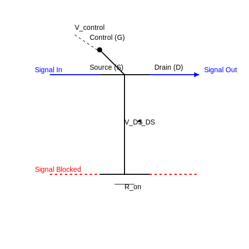
Clipping and Clamping Circuits
1. Definition and Purpose of Clipping Circuits
1.1 Definition and Purpose of Clipping Circuits
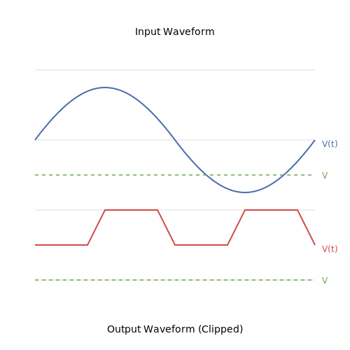
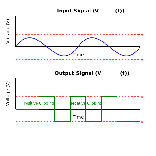
Clipping circuits play a crucial role in electronics, primarily used to limit the voltage levels of signals. These circuits are designed to remove portions of a waveform that exceed specific voltage levels, effectively shaping the signal while preserving its essential characteristics. The process of clipping can be likened to truncating the peaks of a signal, ensuring that it remains within a pre-defined range.
At its core, a clipping circuit functions by establishing a voltage threshold, which can manifest as either a positive or negative limit, depending on the application. When the input signal exceeds this threshold, the output is essentially "clipped" to the level of the threshold, providing a controlled output that helps prevent distortion and potential damage to subsequent circuitry.
Types of Clipping Circuits
The two main types of clipping circuits are:
- Positive Clipping: This variant clips the positive peaks of an AC signal, enabling only the negative portions to pass through. It is particularly useful in signal processing applications where only negative values are valid.
- Negative Clipping: Conversely, negative clipping removes the negative portions of the waveform, allowing only positive values to be transmitted. This type is commonly employed in rectification applications.
The Mathematical Foundation
To understand how clipping circuits operate, let's delve into their mathematical representation. Consider an input voltage signal represented as:
where \(A\) is the amplitude, \(\omega\) is the angular frequency, and \(t\) is time. In a clipping circuit, we define a threshold voltage \(V_{t}\). The modified output voltage \(V_{out}(t)\) after clipping can be described mathematically as follows:
This equation provides a complete representation of how the output changes based on the input signal relative to the threshold voltage. It enables engineers to design circuits that can effectively manage signals without incurring distortion or loss of information.
Real-World Applications
The utility of clipping circuits extends into numerous practical applications, including:
- Signal Processing: Used in audio electronics to limit the voltage levels and prevent distortion in amplifiers.
- Overvoltage Protection: Serves as a protective measure in circuits to limit the maximum voltage that can be applied to sensitive components.
- Digital Signal Communication: Clipping helps ensure that signals remain within the acceptable range for transmission over various media.
In conclusion, clipping circuits are invaluable tools in electrical engineering, facilitating the control of voltage levels and preserving the integrity of signals across various applications. Understanding these circuits is fundamental for designing robust electronic systems that can withstand or manage extreme situations while maintaining high-performance standards.
1.2 Types of Clipping Circuits
Clipping circuits play a crucial role in electronic signal processing by modifying the waveform to fit within specific amplitude limits. They find extensive usage in audio systems, telecommunications, and various measurement applications. The classification of clipping circuits primarily depends on their configuration and operational characteristics. In this section, we will delve into the two primary types of clipping circuits: series clipping circuits and parallel (shunt) clipping circuits. Each configuration has its unique applications and characteristics, making it essential to understand both.
Series Clipping Circuits
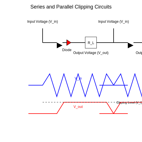
Series clipping circuits are configured in such a way that the input signal passes directly through the clipping device, typically a diode, which is connected in series with the load. The key operational principle is that the diode will only conduct when the input signal exceeds a predetermined voltage level, thus "clipping" the peaks of the waveform.
Mathematically, consider a simple series clipping circuit using a single diode with a forward voltage drop of Vf. The output voltage Vout can be described as:
Here, Vin is the input voltage. This equation emphasizes that any input signal exceeding the threshold set by Vf will have its peaks clipped, thereby protecting subsequent components in a circuit from excessive voltage. Practical applications include protecting amplifiers in audio systems, where signal peaks may otherwise cause distortion or damage.
Parallel Clipping Circuits
In contrast, parallel clipping circuits feature the clipping device, often a diode or a zener diode, connected across the load. This configuration allows the clipping action to occur by conducting excess voltage directly to ground or to the supply voltage when the input signal exceeds a certain threshold. Zener diodes, in particular, are favored for their ability to maintain a fixed breakdown voltage while allowing a reverse current to flow.
The operation of a parallel clipping circuit can be defined by the following equations. For a simple circuit using a zener diode, the output voltage again obeys the property:
In this case, Vz represents the zener breakdown voltage. The output remains equal to the input until the voltage threshold is surpassed, at which point the zener clamps the voltage to Vz. These parallel clipping circuits are extensively utilized in voltage regulation applications, protecting sensitive electronics from overvoltage scenarios.
Understanding the dynamics of series and parallel clipping circuits is foundational for various applications in modern electronics, particularly in signal processing and protection mechanisms. Their implementation allows engineers to design robust systems capable of withstanding unpredictable voltage transients while maintaining signal integrity.
In summary:
- Series Clipping Circuits: Used to control the amplitude of signals, protecting downstream components from overvoltage.
- Parallel Clipping Circuits: Often employed in voltage regulation, useful for clamping down overvoltages to safe levels.
1.3 Characteristics of Clipping Circuits
Clipping circuits serve as essential components in the design of various electronic systems, allowing engineers to shape signals for desired characteristics. These circuits effectively limit the amplitude of a signal by "clipping" portions that exceed a predefined threshold, demonstrating unique features and applications that differentiate them within the realm of electronics.Understanding Clipping Behavior
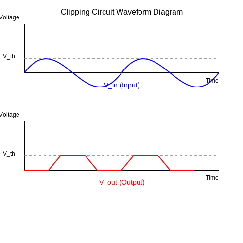
At the heart of a clipping circuit's functionality lies its ability to transition between linear and nonlinear operation. An ideal clipping circuit will yield a piece of the waveform that is either fully retained or completely removed, depending on its design parameters. For instance, in the case of an ideal diode clipper, any input voltage exceeding a certain threshold will be clipped off, resulting in a modified output waveform. This behavior can be illustrated mathematically using piecewise functions or employing voltage limiters during analysis. Let's denote the input voltage as \( V_{in} \) and the clipping threshold as \( V_{th} \). The output voltage \( V_{out} \) can be described by the following piecewise function:Types of Clipping Circuits
Clipping circuits can be categorized based on operational parameters and configurations, primarily into two types:- Positive Clipping Circuits: These circuits limit the positive half of the waveform. For instance, in applications involving audio processing, positive clipping can prevent amplifier saturation and distortion.
- Negative Clipping Circuits: These serve to cut off the negative part of the waveform. In communications, negative clipping is often employed to maintain signal integrity while transmitting data.
Applications of Clipping Circuits
The practical implications of clipping circuits extend across various sectors: 1. Signal Conditioning: Clipping is frequently utilized in signal conditioning to limit voltage levels to within operational thresholds, ensuring proper signal processing by downstream devices. 2. Protective Measures: In power electronics, clipping circuits can protect sensitive components from overvoltage conditions by ensuring voltages remain within tolerable limits. 3. Waveform Shaping: In communications, clipping is employed to shape signals for better transmission characteristics or to ensure compatibility with certain formats. 4. Audio Processing: In audio applications, such as guitar pedals or effects units, clipping modifies sound waves to achieve desirable distortion effects, thereby creating a unique auditory experience.Conclusion
In summary, clipping circuits exhibit distinctive characteristics and play a pivotal role in numerous electronic applications. Understanding their working principles, types, and real-world applications is vital for engineers and researchers aiming to leverage these circuits effectively. For any technical query or further exploration into the practicalities of clipping and its characteristics, the following resources will serve as invaluable references.- Electronics Tutorials - Diode Clipping Circuits — This resource provides a comprehensive overview of diode clipping circuits, including examples and applications.
- Circuit Analysis - Clippers — A breakdown of clipping circuits, providing foundational knowledge enhanced by visual diagrams.
- Clipping Circuits - NI — This white paper from National Instruments dives into practical applications of clipping circuits in various engineering domains.
- EDA Tools - Clipping Circuit Analysis — An interactive platform focused on the analysis and design of clipping circuits, offering tools for simulation.
- Clipping Circuits Explained — A detailed explanation of the principles behind clipping circuits along with practical examples and use cases.
- All About Circuits - Clipping and Clamping Circuits — A tutorial segment dedicated to providing insights on clipping and clamping circuits with exercises for self-study.
- TutorialsPoint - Clippers in Analog Electronics — An extensive resource for understanding various types of clippers and their operational parameters.
2. Basic Components of Clipping Circuits
2.1 Basic Components of Clipping Circuits
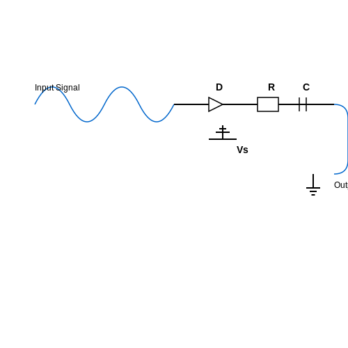
Clipping circuits play a fundamental role in managing voltage levels in various signal applications. The aim is to manipulate the waveform of a signal, either removing portions of it or restricting its peaks. To construct a clipping circuit, several components are essential, each serving a specific function that contributes to the overall performance of the circuit.
Diodes
At the heart of most clipping circuits lies the diode, a device that conducts current primarily in one direction. When forward-biased, it allows current to flow through, while reverse-bias inhibits current. This property makes diodes ideal for clipping voltage levels. For instance, a silicon diode has a forward voltage drop of approximately 0.7V, which is crucial to understand when designing circuits for clipping around specific voltage levels.
Types of Diodes Used
- Standard Signal Diodes: Commonly 1N4148, suitable for low-power applications.
- Schottky Diodes: Known for their low forward voltage drop and fast switching, ideal for high-frequency applications.
Resistors
In combination with diodes, resistors help to set the clipping voltage level by forming a voltage divider with the input signal. The configuration affects the characteristics of the clipping action, including the onset voltage and the steepness of the clipping curve. Proper selection of resistor values is needed to achieve the desired clipping threshold.
Capacitors
While not always necessary, capacitors may be employed in certain clipping configurations to filter noise and stabilize the signal. They can be used in conjunction with resistors to form RC networks that determine the frequency response of the clipping action.
Power Supply
Every clipping circuit requires a well-defined power supply. Understanding the supply voltage is critical, as it dictates the maximum voltage level the diodes are allowed to clip. Proper voltage selection ensures that the clipping action occurs within the operating range of the circuit components, preventing damage or unpredictable behavior.
Practical Example: Clipping Circuit for Audio Signals
A common application of clipping circuits is in audio processing, where they are used to prevent distortion at higher volumes. For instance, in an audio amplifier, the use of clipping circuits ensures that the output signals do not exceed the limits of the component ratings, providing cleaner sound and sustained quality. When designing such circuits, one must carefully select and arrange the components to suit the audio frequency range and the desired gain characteristics.
In conclusion, understanding the basic components of clipping circuits, including diodes, resistors, capacitors, and the power supply, is essential for engineers and researchers looking to design effective signal processing systems. Each component's selection and configuration significantly influence the circuit's performance and reliability.
2.2 Circuit Analysis Techniques
Understanding clipping and clamping circuits requires a solid foundation in circuit analysis techniques. These techniques enable engineers and researchers to model the behavior of circuits, predict their responses, and optimize their design for specific applications. In this section, we'll explore several critical analysis methods, including Thevenin's and Norton's theorems, superposition, and phasor analysis, emphasizing their applications in the context of clipping and clamping circuits.
Thevenin's and Norton's Theorems
Thevenin's and Norton's theorems are fundamental tools that simplify complex linear circuits into simpler equivalent circuits. Theorems are particularly useful when analyzing circuits with non-linear devices like diodes, as they streamline the process of understanding how the circuit behaves under various input conditions.
Thevenin's Theorem states that any linear circuit with voltage sources and resistances can be replaced by a single voltage source (Vth) in series with a single resistance (Rth). The equivalent voltage is determined by finding the open-circuit voltage across the terminals of interest.
To find the Thevenin resistance, Rth, we turn off all independent sources and calculate the total resistance seen from the open terminals.
Alternatively, Norton's Theorem states that a linear circuit can be simplified to a current source (In) in parallel with a resistance (Rn). The Norton current is the short-circuit current flowing through the terminals.
This duality allows for flexibility in analysis; one can choose the representation (Thevenin or Norton) that best simplifies the calculation at hand.
Superposition Theorem
The superposition theorem offers a systematic approach to circuit analysis, allowing one to analyze circuits with multiple sources individually. The principle states that the response in any linear circuit with multiple independent sources is the sum of the responses caused by each source acting alone. This is especially relevant when assessing clamping circuits where the behavior varies based on input voltage levels.
To apply this theorem:
- Turn off all but one independent source (replace independent voltage sources with short circuits and current sources with open circuits).
- Analyze the circuit to find the output voltage or current due to the active source.
- Repeat for all independent sources.
- Sum all individual contributions to obtain the total response.
This method is particularly beneficial in clipping circuits where multiple sources might affect the waveform being clipped. Each source can be analyzed individually, allowing for intricate control of output characteristics.
Phasor Analysis
In AC circuits, phasor analysis significantly simplifies calculations involving sinusoidal waveforms. Phasors transform time-domain sinusoidal signals into complex numbers, enabling the use of algebraic methods instead of differential equations. This method is particularly crucial in clamping circuits designed to manipulate AC signals.
The voltage and current can be represented as:
where Vm and Im are the maximum voltage and current amplitudes, respectively, and ω is the angular frequency. The use of phasors allows for straightforward application of Ohm's Law in the frequency domain:
where Z is the complex impedance of the circuit. For clamping circuits, particularly those involving diodes, phasor analysis can help determine the effective resistance and phase shifts introduced.
In summary, mastering these circuit analysis techniques is not only theoretically enriching but also essential for the practical design and optimization of clipping and clamping circuits in real-world applications, such as signal processing, audio engineering, and telecommunications. As the demand for precision in these areas grows, understanding these foundational methods becomes increasingly crucial for advanced practitioners in the field.
2.3 Designing for Specific Clipping Levels
Understanding Clipping Circuits
Clipping circuits serve as essential tools in managing signal amplitudes, particularly in waveform shaping and protection applications. By preventing a signal from exceeding certain voltage levels, clipping circuits maintain device integrity and appropriate signal integrity. When designing clipping circuits, one must carefully select the clipping levels to address specific requirements of a given application. This section delves into methodologies for achieving defined clipping thresholds.Defining Clipping Levels
Clipping levels can be predetermined based on the operational context of the circuit. These thresholds dictate the maximum amplitude of the output signal and are crucial for maintaining the desired performance characteristics of amplifiers and other electronic devices. For instance, in audio applications, setting the clipping level is imperative to avoid distortion while ensuring the output maintains quality sound reproduction. The voltage levels at which clipping occurs can be determined by the choice of components in the circuit. Typical components include diodes, which conduct current only when the voltage exceeds a certain threshold. The most common form of clipping circuit employs a simple diode configuration which can be analyzed as follows:Diode Clipping Circuit Analysis
Consider a standard diode clipping circuit where a single diode is connected in parallel with the load resistor. The forward voltage drop of the diode, usually around 0.7V for silicon diodes, establishes the threshold at which clipping occurs. When the input voltage exceeds this level, the diode conducts, effectively shunting the excess voltage away from the output. We can express the relationship between the input voltage \( V_{in} \), the diode's forward voltage \( V_D \), and the output voltage \( V_{out} \) using the following equations: 1. For \( V_{in} \geq V_D \): $$ V_{out} = V_D $$ 2. For \( V_{in} < V_D \): $$ V_{out} = V_{in} $$ This establishes that the output voltage will be limited at \( V_D \) whenever the input exceeds the diode's forward threshold. To extend this concept, we can introduce an additional diode in the opposite direction to create a symmetrical clipping effect, thus defining upper and lower clipping levels.Design Considerations
When designing for specific clipping levels, consider how multiple diodes can be combined to optimize performance. For example, using a pair of diodes with different forward voltage drops can create tailored clipping levels for varying signal amplitudes. This is particularly useful in applications such as analog signal processing and audio engineering, where unexpected amplitude fluctuations might lead to unwanted noise or distortion. Factors to consider when specifying clipping levels include:- Input Signal Characteristics: Analyze the expected input signal's amplitude and frequency components.
- Load Impedance: Ensure that the clipping circuit does not adversely affect the load impedance, which might alter signal integrity.
- Thermal Stability: Diodes can heat up, leading to variation in their forward voltage; take this into account when designing for precision.
- Dynamic Range: Balance the clipping levels to retain the details in the useful part of the signal.
Practical Applications
Various practical applications leverage the concepts of clipping and clamping circuits. In digital audio systems, ensuring audio levels do not exceed predefined limits protects amplifiers and speakers. Similarly, in communication channels, clipping circuits can be implemented in the process of signal conditioning to maintain signal integrity and prevent saturation. Moreover, in protection circuits for power amplifiers, clipping thresholds can safeguard against overload conditions ensuring longevity and reliability of the system. Recognizing the significance of precise clipping levels makes designing these circuits both a science and an art, particularly in high-performance applications where fidelity is critical. By understanding the fundamental principles and methodologies involved in designing clipping circuits, engineers can effectively tailor these circuits to meet specific requirements across a range of applications, thus enhancing the reliability and functionality of electronic devices.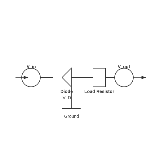
3. Definition and Purpose of Clamping Circuits
3.1 Definition and Purpose of Clamping Circuits
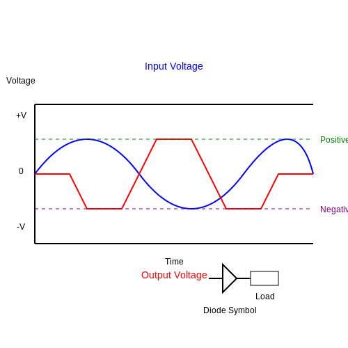
Clamping circuits are fundamental components in the field of electronics, primarily designed to limit the voltage level of a waveform or signal, effectively preventing it from exceeding a specified threshold. This characteristic makes clamping circuits invaluable in protecting sensitive electronic components from voltage spikes that could cause potential damage. The basic operation of a clamping circuit is based on the use of diodes in conjunction with passive components such as resistors and capacitors.
Understanding Clamping Circuits
In essence, a clamping circuit either shifts a waveform vertically to fix its maximum or minimum voltage level or completely eliminates portions of the waveform. The operation typically involves a diode and one or more passive components; when the input signal exceeds the desired limit, the diode conducts, redirecting the excess voltage away from the load. This safeguards downstream circuitry from harmful voltages.
Classifications of Clamping Circuits
Clamping circuits can be classified into two distinct types:
- Positive Clamps: These circuits ensure that the output voltage does not exceed a specified positive level. The most common application is seen in signal processing, where it helps in maintaining signal integrity by preventing saturation.
- Negative Clamps: Conversely, negative clamps restrict the output voltage from dropping below a certain negative threshold. They are crucial in AC circuits to ensure a waveform does not fall below necessary operational bounds.
Practical Applications
The importance of clamping circuits extends beyond textbook definitions, finding applications in various realms, including:
- Signal Processing: In telecommunications, clamping circuits maintain signal levels to avoid distortion, thereby ensuring clear communication.
- Power Supply Regulation: By preventing voltage surges, clamping circuits play an essential role in stabilizing output voltage in power systems.
- Overvoltage Protection: In consumer electronics, clamping circuits protect delicate components from sudden voltage spikes, enhancing device longevity.
In conclusion, clamping circuits not only illustrate foundational electronic principles but also demonstrate practical importance across diverse applications, ensuring reliability and functional integrity in electronic systems. As we delve further into our tutorial, understanding the principles of clamping circuits will provide a solid basis for exploring more complex topics in electronics, such as clipping circuits and their combined use in signal conditioning.
3.2 Types of Clamping Circuits
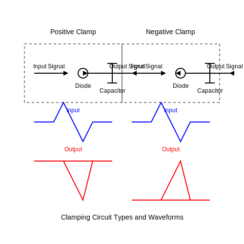
Clamping circuits serve as indispensable tools in electronics, especially when it comes to signal conditioning. These circuits are designed to shift the voltage levels of an incoming signal to a specified range, effectively safeguarding sensitive components from over-voltage conditions. Clamping circuits are primarily classified into three types: positive clamping circuits, negative clamping circuits, and double clamping circuits. Understanding each type allows for effective application across a broad spectrum of electronic systems.Positive Clamping Circuits
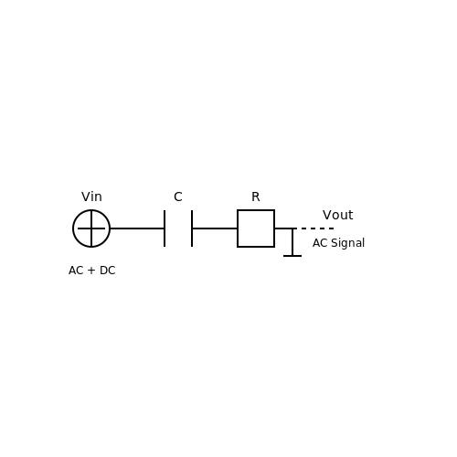
A positive clamping circuit is intended to elevate the input voltage waveform such that the entire signal is shifted upwards. This type of circuit typically employs a diode, a capacitor, and a resistor. When the input signal becomes positive, the diode becomes forward-biased, allowing current to flow. The capacitor charges to the peak positive voltage level of the input signal, maintaining this elevated level even when the input drops below zero. Using the following parameters: - Voltage threshold (Vt) - Input signal voltage (Vin) We can derive the output voltage (Vout): 1. During positive half-cycles: $$ V_{\text{out}} = V_{\text{in}} + V_t $$ 2. During negative half-cycles: $$ V_{\text{out}} = 0 $$ This behavior effectively clamps the negative portion of the waveform to zero volts, making it suitable for interfacing with analog-to-digital converters (ADCs) to avoid distortion.Negative Clamping Circuits
Conversely, negative clamping circuits serve to lower the input signal voltage. Similar to positive clamping, this configuration employs a diode, capacitor, and resistor but in a reverse bias setup. When the input signal goes negative, the diode will conduct in the opposite direction, leading the capacitor to discharge. Around the same parameters as above: - Voltage threshold (Vt) - Input signal voltage (Vin) For this setup, the output voltage can be defined as follows: 1. During negative half-cycles: $$ V_{\text{out}} = V_{\text{in}} - V_t $$ 2. During positive half-cycles: $$ V_{\text{out}} = 0 $$ This arrangement makes negative clamping circuits vital in protecting downstream components from excessive negative voltages.Double Clamping Circuits
Double clamping circuits introduce the idea of clamping for both the positive and negative halves of an input waveform. This is achieved through the use of two diodes, capacitors, and potentially two resistors. The output voltage in a double clamping circuit is characterized as such: - Positive half-cycle: $$ V_{\text{out}} = V_{\text{in}} + V_t $$ - Negative half-cycle: $$ V_{\text{out}} = V_{\text{in}} - V_t $$ This type of clamping circuit is especially beneficial in systems where it is crucial to maintain signal integrity across both voltage polarities, ensuring that the output waveform does not exceed specific upper or lower bounds. Understanding the operational principles of these varying clamping circuits allows engineers and researchers to apply the correct configuration based on the signal conditions they anticipate encountering in their work. This application ranges from professional audio systems, where distortion must be avoided, to digital signal processors where voltage thresholds must be strictly adhered to.Practical Implications and Applications
In practical scenarios, these clamping circuits are critical in applications such as: - Signal conditioning in sensor interfaces - Protection circuits in power supplies - Waveform shaping in analog signal processing Advancements in semiconductor technologies have rendered clamping circuits more efficient and cost-effective. This has prompted their increased usage in high-speed digital applications and high-frequency designs, making it essential for modern engineers to be adept in their application. In summary, the delving into various types of clamping circuits illustrates not only their fundamental design characteristics but also their critical importance in managing electrical signals across a variety of applications. The effectiveness of these circuits in protecting components emphasizes their role in enhancing the reliability of electronic systems.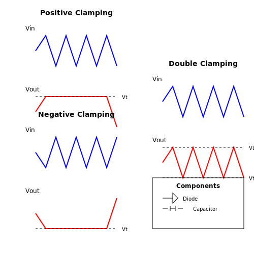
3.3 Characteristics of Clamping Circuits
Clamping circuits play a crucial role in electronics, acting as precise tools for managing voltage levels in various applications. Their primary function is to shift a waveform to a different level, without altering its shape. This ability imparts several significant characteristics that are vital for designing circuits that require specific voltage ranges. Understanding these characteristics is essential for engineers and researchers when integrating clamping circuits into complex systems.
Functionality of Clamping Circuits
A clamping circuit can be constructed using diodes, capacitors, and resistors, forming a simple yet effective configuration. The fundamental operation involves the diode's conduction properties, which allow the circuit to modify the input signal's baseline without distortion. Typically, clamping circuits can be classified into two types: positive clamps, which elevate the waveform above the zero-volt level, and negative clamps, which lower it. This shifting of voltages makes clamping circuits invaluable in protecting sensitive components from voltage spikes and conditioning signal levels.
Key Characteristics
The characteristics of clamping circuits are defined by several parameters that dictate their performance in real-world applications:
- Voltage Levels: The output voltage levels of clamping circuits are primarily determined by the configuration and the orientation of the diodes used. The diode's forward voltage drop impacts the clamping voltage.
- Response Time: The speed at which a clamping circuit can respond to changes in voltage is critical in high-speed applications. Fast diodes, such as Schottky diodes, are often employed to minimize delay.
- Frequency Response: Clamping circuits are affected by the frequency of the input signal. Understanding the circuit’s frequency response is essential, particularly in RF applications, where attenuation of certain frequencies may occur.
- Temperature Coefficients: The performance of diodes in clamping circuits can vary with temperature. Engineers must account for these variations in their designs, especially in environments subject to fluctuating temperatures.
Practical Applications
Clamping circuits find practical usage across various industries. For instance, in analog signal processing, clamping circuits are employed to establish specific voltage limits for signals before they enter more sensitive stages of amplification or processing. In telecommunications, these circuits help maintain voltage levels that align with digital signaling requirements, ensuring data integrity during transmission.
Moreover, clamping circuits are regularly utilized in voltage surge protection devices to safeguard electronic equipment from overvoltages. By effectively shifting the voltage to safe levels, clamping circuits significantly enhance the longevity and reliability of components.
Conclusion
In summary, understanding the characteristics of clamping circuits is indispensable for designing efficient and robust electronic systems. Their ability to control voltage levels precisely makes them essential in various applications, from signal conditioning to protection circuits. As technology advances, the continued exploration of clamping circuits will unveil further innovations and optimizations, reinforcing their significance in modern electronics.
4. Basic Components of Clamping Circuits
4.1 Basic Components of Clamping Circuits
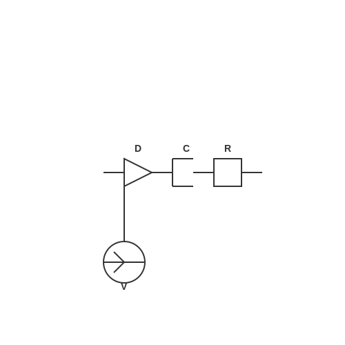
Clamping circuits are fundamental in electronics, designed to alter the voltage level of a signal without affecting its waveform shape. The primary objective of these circuits is to shift the entire waveform up or down so that it stays within designated limits. To achieve this functionality, a few basic components are essential. Understanding these components allows engineers and researchers to design efficient clamping circuits tailored for various applications.
Diodes
The diode is the cornerstone of any clamping circuit. Its ability to conduct current in one direction while blocking it in the opposite direction enables the creation of the biasing necessary for clamping. When used in clamping circuits, the diode controls the voltage across the load based on its orientation and the power source voltage.
In practical applications, diodes can be chosen based on specific requirements, such as:
- Forward voltage drop: This is the minimum voltage required for the diode to conduct. Silicon diodes typically have a drop of about 0.7V, while Schottky diodes may have a lower drop (0.2 to 0.3V), making them preferable for high-speed applications.
- Reverse recovery time: This parameter is crucial in high-frequency applications, as it affects switching speed and efficiency.
Capacitors
Capacitors play a dual role in clamping circuits. Firstly, they serve as coupling elements that block DC components while allowing AC signals to pass through. Secondly, they can help stabilize the voltage level that the diode sets, essentially "holding" the shifted voltage for some duration.
Key attributes of capacitors include:
- Capacitance value: This defines how much charge the capacitor can store, directly influencing the circuit's response time and the degree of clamping.
- Voltage rating: It is imperative that the capacitor’s voltage rating exceeds the maximum voltage it will encounter in the circuit to avoid breakdown.
Resistors
While resistors do not directly influence the clamping effect, they play a critical role in controlling the overall current flow in the circuit. By limiting the current, resistors help in protecting components from overload and ensuring the clamping action occurs smoothly without abrupt voltage spikes.
Some considerations for using resistors in clamping circuits include:
- Resistance value: A higher resistance value will limit current more, impacting how quickly the circuit reacts to changes in input voltage.
- Power rating: Similar to capacitors, it's essential to ensure that resistors can handle the power dissipation without thermal failure.
Voltage Sources
Finally, clamping circuits often require a reference voltage. This can be provided by independent DC sources or integrated into the circuit design using other components such as Zener diodes to create stable reference points.
In summary, the effective functioning of clamping circuits hinges upon the judicious selection and integration of these components. Engineers and researchers must consider not only the specifications of individual components but also how they work together to achieve the desired clamping effect. This understanding lays a robust foundation for developing more intricate circuits and systems that depend on precise voltage management.
4.2 Circuit Analysis Techniques
Analyzing clipping and clamping circuits requires a strong foundation in both circuit theory and the behavior of semiconductor devices. In this section, we will explore some essential circuit analysis techniques, focusing on the application of linear approximations, piecewise linear analysis, and methods involving operational amplifiers (op-amps).
Piecewise Linear Approximation
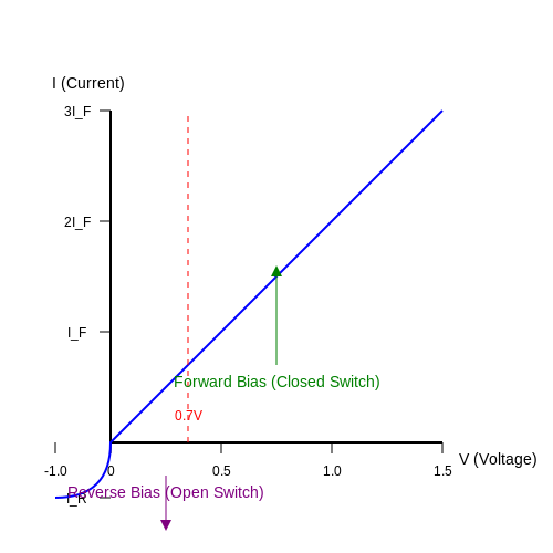
Clipping and clamping circuits often involve non-linear components, such as diodes, which complicate analysis. To handle these complexities, we employ the piecewise linear approximation method. This approach simplifies the analysis by representing the diode's I-V characteristic as a series of linear segments.
For example, in the forward bias region, a diode can be approximated as a closed switch for voltages above the threshold voltage (typically around 0.7V for silicon diodes), and in the reverse bias region, it can be treated as an open switch. These approximations lead to different circuit configurations depending on the input signal. A graphical representation of this I-V curve can be beneficial in visualizing the behavior of the diode:
In this equation, \( I_S \) is the reverse saturation current, \( V \) is the voltage across the diode, \( n \) is the ideality factor, and \( V_T \) is the thermal voltage. Under the piecewise linear model, the diode can be represented as:
- Open Circuit for \( V < 0.7V \).
- Voltage source of 0.7V for \( V \geq 0.7V \).
Thevenin's and Norton's Theorems
Both Thevenin's and Norton's theorems simplify the analysis of complex circuits by allowing the replacement of large network views with simpler equivalents. In a clipping or clamping circuit, this equivalency can significantly ease calculations of voltages and currents across specific components.
Using Thevenin's theorem, we can derive the Thevenin equivalent circuit by finding:
- The Thevenin voltage (\( V_{TH} \)) across the load.
- The Thevenin resistance (\( R_{TH} \)) seen from the load side.
Once these values are established, the behavior of the entire circuit can be analyzed as a simple voltage source in series with a single resistance.
Operational Amplifiers in Clipping Circuits
Operational amplifiers (op-amps) are often employed in clipping circuits to achieve sharper transitions and a more controlled clipping effect. Their ability to operate in different configurations—such as inverting, non-inverting, or comparator modes—allows for versatile circuit designs.
To analyze an op-amp-based clipping circuit, we apply the concept of feedback. The op-amp output voltage ranges are determined by the feedback network, and the precise clipping levels can be adjusted by modifying component values around the feedback path.
A common circuit example is the Schmitt trigger configuration, which can be visualized as follows:
This configuration demonstrates how hysteresis can effectively manage the noise margins, ensuring that the clip occurs only when certain voltage thresholds are crossed.
Frequency Domain Analysis
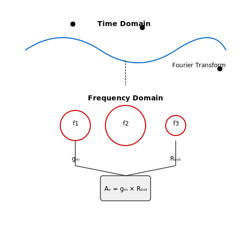
When dealing with high-frequency signals in clipping and clamping circuits, understanding the frequency response becomes of utmost importance. Analyzing these circuits in the frequency domain using Bode plots or Nyquist plots can reveal insights about the circuit's behavior under varying input frequencies. Components such as capacitors and inductors introduce phase shifts and attenuations that significantly impact the clipping level.
By employing these analysis techniques, engineers can design robust clipping and clamping circuits optimized for specific applications, ensuring reliable performance across a range of operating conditions.
4.3 Designing for Specific Clamping Levels
When designing clamping circuits, one of the essential parameters to control is the clamping level. This subsection aims to explore how to design clamping circuits that can effectively manage specific voltage levels while ensuring minimal distortion to the input signal. Understanding the design principles behind achieving different clamping levels is crucial for applications ranging from signal processing to power electronics.Understanding Clamping Levels
In essence, a clamping circuit is designed to limit the maximum (or minimum) voltage of a waveform to a predetermined level. This is achieved using diodes, which conduct when certain thresholds are exceeded. The clamping level is the voltage at which the diode begins to conduct, effectively “clamping” the waveform. For example, if a circuit is designed to clamp at +5V, any input voltage exceeding this will be clipped to +5V. A common clamping configuration utilizes a diode in conjunction with a resistor and capacitor. The placement of these components dictates the clamping behavior. Let's delve into the mathematical details for determining specific clamping levels.Mathematical Modeling of Clamping Circuits
Consider a simple positive clamping circuit that uses a diode (D), resistor (R), and a capacitor (C) in series. The clamping voltage can be expressed mathematically, taking into account forward bias conditions of the diode characterized by its forward voltage drop, typically denoted as \( V_f \). 1. Circuit Configuration: The clamping circuit can be represented as follows: - Input Voltage (Vi) - Diode (D) - Resistor (R) - Capacitor (C) - Output Voltage (Vo) 2. Voltage Equations: When the diode conducts, the output voltage \( V_o \) will be defined as: $$ V_o = V_i - V_f $$ where \( V_f \) is the forward voltage drop across the diode. 3. Capacitor Behavior: The capacitor charges to the clamping voltage. When the input exceeds this voltage: $$ V_o(t) = V_{clamp} + (I(t) R) $$ where \( I(t) \) is the current flowing through the resistor. 4. Clamping Level Design: To achieve a specific clamping level \( V_c \), the following relationship must hold true: $$ V_{clamp} = V_c + V_f $$ Thus, to design for a specific clamping voltage, you must choose the \( V_f \) of the diode accordingly.Practical Designing Considerations
When designing clamping circuits for specific clamping levels, engineers must consider several practical factors:- Diode Selection: Choose diodes with appropriate \( V_f \) characteristics. Silicon diodes typically have a \( V_f \) of 0.7V, while Schottky diodes can be as low as 0.3V.
- Resistor and Capacitor Values: Adjusting the values of R and C will determine the charging time and the stability of the clamping action.
- Signal Frequency: The frequency of the input signal affects the charging and discharging rates of the capacitor, influencing the overall circuit response.
- Thermal Characteristics: Ensure that both the diode and resistor can handle power dissipation without overheating, particularly under high signal conditions.
Real-World Applications
The design principles outlined here have far-reaching implications in various fields: - Communication Systems: Clamping circuits are employed to protect sensitive components from voltage spikes in RF circuits. - Power Electronics: They help prevent over-voltage conditions in switch-mode power supplies (SMPS) by clamping transient voltages. - Signal Processing: Clamping is vital in analog signal processing to maintain signal integrity while conditioning signals for further processing. Understanding how to design clamping circuits for specific voltage levels allows engineers to integrate these components effectively, leading to more robust and reliable electronic systems.5. Signal Processing Applications
5.1 Signal Processing Applications
The realms of signal processing have witnessed significant advancements due to the utilization of clipping and clamping circuits. These circuits, although simple in design, serve critical functions across various applications, ranging from audio systems to communication technologies, thus bolstering the overall functionality and fidelity of signal processing systems.Understanding Clipping Circuits
Clipping circuits are designed to restrict the amplitude of a signal to a specific level. When the input voltage exceeds a predetermined threshold, the circuit 'clips' the waveform, effectively altering its shape while preserving the integrity of the original signal within the specified range. This process is crucial in applications where avoiding distortion during signal amplification is paramount. For example, in audio systems, clipping can prevent distortion by limiting the amplitude of high-level signals that would otherwise push amplifiers beyond their linear operating range. By ensuring that signals do not exceed a certain threshold, clipping circuits help maintain audio quality, particularly important in live sound environments and high-fidelity audio systems.Types of Clipping Circuits
Clipping circuits can be classified primarily into two categories: hard clipping and soft clipping.- Hard Clipping: Often implemented through diodes, hard clipping abruptly truncates the peaks of a signal, leading to a significant alteration in its waveform. This result is prevalent in various electric guitar effects, where distortion is desirable for tonal shaping.
- Soft Clipping: This technique gradually compresses the signal, resulting in a more pleasant auditory outcome. Soft clipping circuits typically use transistor-based configurations, providing a smoother transition at the clipping threshold, which is often sought in audio mastering applications.
Exploring Clamping Circuits
Clamping circuits, on the other hand, function to adjust the DC level of an AC waveform, effectively shifting its baseline without altering its shape. This is particularly useful for ensuring signals remain within the operational range of subsequent components, particularly in analog-to-digital converters (ADCs) and other signal processing units. For instance, in a digital communication system, clamping circuits can stabilize the input signal's DC offset, allowing for more reliable detection and digitization of the information being transmitted. This ensures that fluctuating signal levels do not lead to erroneous data representations.Practical Applications in Signal Processing
Real-world applications of clipping and clamping circuits are both varied and significant:- Audio Signal Processing: In amplifiers, dynamic range compression techniques utilize clipping to maintain sound quality by avoiding driver overloads. This is vital for any audio-related technology where clarity and fidelity are essential.
- Data Communication: Clamping is prevalent in modulated signals to eliminate baseline shifts, ensuring accurate data retrieval at the receiver end, especially in serial communication systems.
- Image Processing: In graphical systems, similar principles apply. Clipping circuits can enhance image contrast by limiting brightness ranges, while clamping circuits can normalize pixel intensity levels across varying lighting conditions.
Conclusion
In summary, clipping and clamping circuits are pivotal in enhancing signal integrity across numerous applications. Their ability to manipulate signal amplitudes and DC levels effectively safeguards against distortion and operational failures. By understanding the dynamics of these circuits, engineers and researchers can leverage their capabilities to improve the quality and reliability of signal processing systems. As technology progresses, the sophistication and integration of these circuits in modern developments continue to grow, promising exciting opportunities for innovation in the field.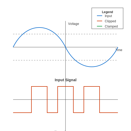
5.2 Protection Circuits in Electronics
Protection circuits play a pivotal role in preserving the integrity and functionality of electronic systems by safeguarding them against adverse conditions, such as voltage spikes, surges, and various overload situations. These circuits ensure that the components remain within their specified limits, preventing potential failure or damage. In this section, we will delve into the mechanisms of clipping and clamping circuits as essential protection elements in electronic devices.
Understanding Clipping Circuits
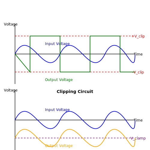
Clipping circuits are designed to limit the voltage at their output by "clipping" the waveform signals that exceed a predefined threshold. These circuits are commonly integrated into amplifiers and audio systems to prevent signal distortion and protect downstream components.
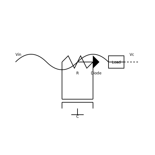
To examine the principles of clipping, consider a simple RC circuit consisting of a resistor and a diode configured to clip positive voltage peaks:
The diode conducts once the input voltage exceeds the diode's forward voltage drop (approximately 0.7 V for silicon diodes), effectively "clipping" any peaks above this threshold. The output waveform, therefore, remains constrained to a defined range, which results in the suppression of signal distortion.
Here, \( V_D \) represents the threshold voltage of the diode. For practical applications, these circuits are vital in audio processing equipment and communication systems where signal integrity is paramount.
Utilizing Clamping Circuits
In contrast to clipping, clamping circuits maintain the integrity of the waveform while shifting the baseline level. This functionality is crucial in applications where it is necessary to prevent negative voltages or to reposition the waveform within a desired voltage range. Clamping circuits often utilize combination arrangements of diodes and capacitors.
Take, for example, a negative clamp circuit that employs a diode connected to the ground. When the input signal attempts to go below zero volts, the diode becomes forward-biased and conducts, effectively raising the voltage output to zero volts. The response of the circuit can be described mathematically as follows:
This clamping action is crucial in protecting sensitive components in digital circuits, preventing damage due to negative voltage excursions and ensuring that signals remain within the operational ranges of logic devices.
Real-World Applications and Considerations
Both clipping and clamping circuits find extensive applications across various domains of electronics. In power supply design, these circuits mitigate transients due to capacitive loads or sudden switching. In audio electronics, they are invaluable for shaping the dynamics of sound signals, improving overall sound fidelity by reducing clipping distortion. Furthermore, protective measures can enhance the robustness of microcontroller inputs against voltage spikes.
It’s essential to note that while these circuits provide critical protection, they must be carefully designed to avoid unintended consequences like unwanted frequency responses or signal degradation. Designers often perform simulations and utilize SPICE models to refine circuit parameters prior to implementation.
In summary, clipping and clamping circuits serve as foundational elements in electronic protection schemes, ensuring signal integrity and safeguarding components from operational hazards. Their understanding and application can significantly enhance the longevity and reliability of electronic systems in diverse applications.
5.3 Practical Examples and Case Studies
To understand the operational principles and applications of clipping and clamping circuits, it proves beneficial to examine a selection of practical examples and case studies. These real-world scenarios reveal how these circuits function and address specific engineering challenges through practical implementations.
Clipping Circuit Example in Audio Signal Processing
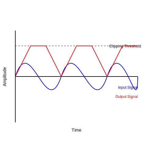
One of the most common applications of clipping circuits is in audio signal processing, particularly when aiming to limit the amplitude of audio signals to prevent distortion. In this case, a simple diode-based clipping circuit can be utilized. Consider a scenario where the output of an audio amplifier might exceed the limits of speakers, leading to potential damage. By implementing a clipping circuit, we can set a maximum output voltage level.
The circuit comprises an op-amp configured in a non-inverting setup, with diodes connected across the output. When the output signal amplitude exceeds the forward voltage of the diodes, they conduct, effectively clamping the output signal to safe levels. This ensures that the audio remains clean without severe distortion while protecting the speaker from damage due to over-voltage.
Here, \( V_{D} \) represents the forward voltage drop of the diodes, critical for determining the clipping level of the circuit.
Case Study: Voltage Clamp in Power Management Systems
Voltage clamping circuits are widely employed in power management systems to protect sensitive components from voltage spikes. Consider a case study involving a microcontroller unit (MCU) interfaced with various sensors. In this setup, voltage transients could result from load switching or external emissions.
A practical voltage clamp can be established using a Zener diode. This diode is reverse-biased in parallel with the load (MCU). If a voltage spike above a predetermined threshold occurs, the Zener diode conducts, shunting excess current away from the MCU to ground, thereby safeguarding the device from damage.
The selection of the Zener diode's breakdown voltage must align with the operating parameters of the MCU to ensure optimal protection. For instance, if an MCU operates at 5V, a Zener diode with a breakdown voltage of approximately 5.1V would be ideal, ensuring quick response to voltage spikes while maintaining nominal operational conditions.
Where \( I \) is the current flowing through the diode, \( V_{max} \) is the maximum expected voltage, \( V_{Z} \) is the Zener breakdown voltage, and \( R_{series} \) is the resistance in series used to limit the current through the Zener diode when clamping occurs.
Integration into Communication Systems
Clipping and clamping circuits also play a critical role in communication systems to ensure signal integrity. For instance, In data communication, signals often fluctuate due to noise and interference during transmission. Manipulating analog signals to a standard level through clipping circuits enhances the quality before converting them into digital signals via Analog to Digital Converters (ADCs).
In this context, the clipping circuit must be meticulously designed to preserve essential signal features while eliminating excessive voltage levels that could lead to ADC saturation. Engineers often utilize adjustable clipping circuits to facilitate tuning for optimal threshold levels in varying signal environments.
This fine-tuning of threshold levels helps ensure that bit errors are minimized, maintaining high integrity in the data transmission process across noisy channels.
In conclusion, understanding the practical implementations and intricacies involved in clipping and clamping circuits illustrates their applicability in protecting electronic systems, enhancing audio clarity, and maintaining data integrity in communication channels.
6. Identifying Common Problems
6.1 Identifying Common Problems
Understanding clipping and clamping circuits involves recognizing their operational stability and the common impediments they may encounter. These circuits, widely utilized in signal processing, precision rectification, and waveform shaping, can exhibit a range of practical problems that engineers and researchers need to address. Here, we will detail these common issues and their implications, ensuring you are well-equipped to diagnose and resolve them.1. Clipping Circuit Problems
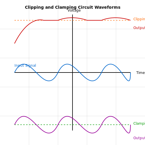
Clipping circuits, used to restrict voltage levels beyond certain thresholds, can encounter several issues:- Signal Distortion: When input signals exceed the designed clipping level, distortion can result. For instance, if a bipolar clipping circuit designed to limit input signals to ±1V is instead fed a 10V signal, the resulting waveform will exhibit clipping and harmonic distortion. This is especially problematic in audio applications where signal fidelity is paramount.
- Thermal Effects: Over time, excessive clipping can cause thermal stress on components like diodes. For example, a diode employed at a high frequency near its maximum current rating can shift its characteristics, leading to increased forward voltage drop and possibly failure.
- Output Loading: The load impedance can significantly affect the performance of clipping circuits. A low impedance load can cause the output voltage to sag, distorting the clipped waveform further. Thus, ensuring appropriate loading conditions is critical for maintaining signal integrity.
2. Clamping Circuit Issues
Clamping circuits serve to shift the voltage level of a waveform. Common problems include:- Voltage Level Drift: Components such as capacitors and operational amplifiers can experience aging effects, leading to unpredictable voltage level shifts over time. For instance, electrolytic capacitors may exhibit leakage, which can alter the clamping level and impact circuit performance.
- Dynamic Range Limitation: If the clamping voltage is not set appropriately with respect to the input signal's peak value, certain portions of the waveform might get clipped. This not only affects the dynamic range but can also limit the utility of the clamping circuit in applications that demand high fidelity.
- Transient Response: The behavior of clamping circuits during transient conditions can be compromised. If an input signal quickly transitions through the clamping threshold, it may not settle properly, resulting in overshoot or undershoot conditions. This is pertinent in high-speed digital circuits where signal integrity is crucial.
3. General Electrical Issues
Both clipping and clamping circuits are subject to general issues such as:- Power Supply Variability: Variations in power supply voltage can significantly impact both clipping and clamping circuits. Fluctuations may lead to unexpected clipping levels or improper voltage shifts, hence maintaining a stable power supply is vital for reliable circuit operation.
- Noise Interference: External electromagnetic interference can cause erroneous behavior in clipping and clamping circuits. Ensuring good grounding practices and shielding can mitigate such issues, enhancing the circuit’s performance.
- Component Nonlinearity: All electronic components have inherent non-linear characteristics, which can lead to deviations from expected circuit behavior. It is important to use high-precision components where applicable to maintain the fidelity of the output.
6.2 Diagnostic Techniques
In the analysis and design of clipping and clamping circuits, diagnostic techniques are crucial for ensuring performance, stability, and functionality. These circuits often serve as necessary components in signal processing applications, where distortion and signal integrity are key concerns. As such, the ability to detect faults, performance issues, and operational parameters can significantly streamline the design process.Understanding Signal Behavior
The first step in a robust diagnostic approach involves the understanding of how a clipping or clamping circuit behaves under various conditions. Clipping circuits intentionally limit the output voltage to specific thresholds, while clamping circuits shift the waveform vertically without altering its shape. When diagnosing performance, engineers must consider the input voltage amplitude, signal frequency, and load conditions. Analyzing the input-output relationship is fundamental. For instance, in a basic clipping circuit utilizing a diode, attaching an oscilloscope can visually reveal how the output signal is shaped. Observations like whether the waveform is correctly clipped following the desired threshold provide insight into the circuit's functionality.Testing Methodologies
For professional engineers, systematic testing methodologies can be employed:- Visual Inspection: Begin with a thorough visual inspection of the circuit to detect physical damage, poor solder joints, or component misplacements. This step may save time before proceeding to electrical measurements.
- Verification of Component Values: Use a multimeter to verify the resistance and capacitance values of individual components against their specified values. Any discrepancy can indicate component malfunction, affecting the circuit's behavior.
- Dynamic Signal Analysis: Employing an oscilloscope, engineers can analyze the frequency response and transient behavior of the circuit. This dynamic testing allows for the assessment of clipping levels, distortion, and recovery times.
- Simulation Verification: Before hardware implementation, utilizing SPICE simulations to model the circuit can identify potential issues with signal integrity and operation. Simulations can help visualize the circuit response in various conditions.
Mathematical Diagnosis
For more advanced diagnostic techniques, employing mathematical models is essential. For instance, when assessing a diode clipping circuit, understanding the voltage transfer characteristics will involve deriving the equation governing the diode's current-voltage relationship. The Shockley diode equation given by: $$ I = I_s \left( e^{\frac{V}{nV_T}} - 1 \right) $$ is pivotal. Here, \( I_s \) is the reverse saturation current, \( V_T \) is the thermal voltage, and \( n \) is the ideality factor. By rearranging this equation, engineers can determine the voltage drop at various input signals. When the input voltage exceeds the specified clip level (let's say \( V_{clip} \)), the output voltage will stay constant at this threshold. The equation can hence be used to predict whether the circuit will operate correctly under expected conditions. Understanding how parameters like temperature affect \( V_T \) allows for further predictions about performance variations under different operational environments. Additionally, a proactive approach includes performing a sensitivity analysis of component tolerances and their effects on clipping and clamping characteristics.Real-World Applications and Case Studies
Real-world applications abound for these diagnostic techniques. In audio equipment, clipping circuits are utilized to prevent signal distortion that can lead to speaker damage. Clamping circuits are employed in digital communication to protect sensitive components from signal transients. An example case study is the design of an audio limiter, where effective diagnostics ensure that dynamic range compression preserves audio quality while preventing clipping during peak amplitudes. In conclusion, the implementation of diagnostic techniques is integral to the successful operation of clipping and clamping circuits. By combining visual inspections, dynamic signal testing, mathematical modeling, and real-world applications, engineers can ensure optimal performance and reliability in their electronic designs.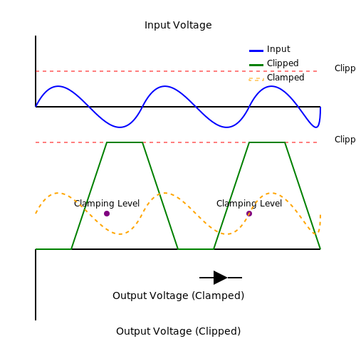
6.3 Solutions and Best Practices
Clipping and clamping circuits are fundamental components in electronic design and signal processing. Their ability to manage voltage levels and protect circuitry from excessive voltages makes them invaluable in a variety of applications. As advanced engineers and researchers, understanding the practical implementation of these circuits is crucial for optimizing their performance and reliability. This section highlights effective solutions and best practices for designing and using clipping and clamping circuits.
Proper Selection of Components
Choosing the right components is the first step toward implementing effective clipping and clamping circuits. This involves selecting diodes, resistors, and capacitors with appropriate ratings:
- Diodes: Use diodes with a low forward voltage drop and high peak inverse voltage (PIV) rating to ensure they perform well under varying conditions. Schottky diodes, for example, are excellent for high-speed applications.
- Resistor Value: The choice of resistor affects the time constant of the clamping circuit. A higher resistor value results in a slower response time, affecting the circuit's ability to respond to rapid voltage spikes.
- Capacitance: In capacitor clamping circuits, selecting the right capacitance (in Farads) is essential to control the response time and filtering capabilities. Large capacitance values can smooth out voltage transients effectively but might slow down circuit reaction.
By carefully selecting these components, the reliability and functionality of the clipping and clamping circuits can be significantly enhanced.
Simulation and Modeling
Before physical implementation, it is advisable to conduct thorough simulations using software tools such as SPICE. These simulations can help predict the behavior of your circuits under different operating conditions:
- Simulation enables the testing of various configurations without the need for physical components, reducing costs and development time.
- Tools like LTSpice or Multisim facilitate visualizing how the circuit responds to inputs and identifying potential failure points.
Employing a simulation environment helps in iterating designs and optimizing the circuit layout before committing to hardware.
Thermal Management
Clipping and clamping circuits may experience thermal stress due to the rapid current flows they handle. Implementing adequate thermal management techniques is critical:
- Heat Sinks: Utilize heat sinks or thermal pads for heat dissipation. This is particularly important if the circuit operates at high power levels.
- Temperature Sensors: Consider incorporating temperature sensors that can trigger protection mechanisms if temperatures exceed safe operating conditions.
Effective thermal management ensures prolonged component life and reliable circuit operation in real-world applications.
Case Studies and Practical Applications
Many industries utilize clipping and clamping circuits in their designs:
- Telecommunications: In telecom infrastructure, these circuits protect sensitive circuit components from voltage spikes caused by lightning or switching events.
- Consumer Electronics: Devices such as televisions and audio systems use clamping circuits to prevent distortion from unexpected signal peaks.
Studying real-world applications further solidifies understanding and inspires innovative designs that leverage the principles of clipping and clamping circuits.
Final Considerations
In conclusion, the design and implementation of clipping and clamping circuits require a careful balance of component selection, thermal management, and validation through simulation. Engineering best practices involve a thorough understanding of both operational principles and practical constraints, ensuring robust and efficient circuit performance.
By continuously exploring new technologies and methodologies while adhering to these standard practices, engineers can enhance circuit reliability and performance in complex electronic systems.
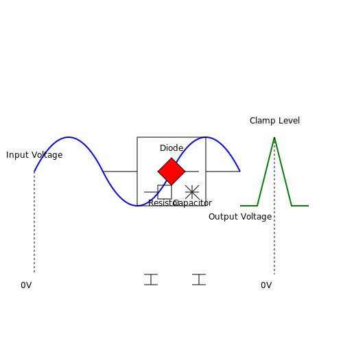
7. Key Textbooks on Clipping and Clamping Circuits
7.1 Key Textbooks on Clipping and Clamping Circuits
- Microelectronic Circuits by Adel S. Sedra and Kenneth C. Smith — This textbook provides comprehensive coverage of electronic circuit design and analysis. The sections on waveform shaping techniques provide essential insights into clipping and clamping circuits.
- Introduction to Modern Electronics by James Fiore — Offering a detailed exploration of electronics fundamentals, this book thoroughly discusses both diode clipping and clamping circuits used in waveform shaping.
- Analysis and Design of Analog Integrated Circuits by Paul R. Gray and Robert G. Meyer — It covers a wide range of analog circuits including clippers and clampers, providing detailed design techniques and practical application guidance.
- The Art of Electronics by Paul Horowitz and Winfield Hill — Known for its intuitive approach, this book simplifies complex electronic principles, with particular chapters dedicated to nonlinear signal processing involving clipping and clamping circuits.
- Analog Electronics by David Crecraft and David Glover — An excellent guide linking theoretical knowledge to practical applications in electronics, featuring detailed analysis of analog circuit functions, including extensive coverage of clippers and clampers.
- Microelectronic Circuits: Analysis and Design by Muhammad Rashid — Offers an analytical approach to microelectronics, focusing on intrinsic device applications like CLAMPING and CLIPPING and their real-world implementations.
- Handbook of Analog Circuit Design by Dennis L. Feucht — This extensive resource book delves into the intricacies of analog circuit designs, providing guidance on non-linear circuit applications such as clippers and clampers.
7.2 Research Papers and Articles
- IEEE Xplore Digital Library — A comprehensive source of scientific and professional knowledge, including peer-reviewed research papers on clipping and clamping circuits for advanced practitioners and researchers in the field.
- Wiley Online Library — Provides access to a wide range of scientific articles, offering in-depth studies and advancements in electronic circuits, including clipping and clamping techniques.
- Journal of Electrical Engineering and Technology — Features research papers in the field of electrical engineering, with articles focusing on theoretical and practical aspects of circuit design including clipping and clamping circuits.
- ACM Digital Library — Offers a vast array of materials, including technical papers and articles, exploring innovative approaches to clipping and clamping circuits among other topics in electronics and hardware design.
- IET Circuits, Devices & Systems — A journal that publishes both theoretical and practical research on electronic circuits and systems, specifically addressing topics like clipping and clamping techniques.
- International Journal of Electronics — Delivers high-quality research articles focusing on developments in electronics, including analyses and improvements in clipping and clamping circuit designs.
- Analog Integrated Circuits and Signal Processing — Publishes articles that deal with the design and tuning of analog circuits, with useful insights into clipping and clamping circuits.
- Microelectronics Journal — Contains research articles and breakthroughs in microelectronics, including comprehensive studies of current technologies in clipping and clamping circuits.
- ScienceDirect — A database offering a vast range of scientific articles covering the developments in electrical and electronics engineering, focusing on practical applications of circuit components like clippers and clamper circuits.
- ACM Transactions on Design Automation of Electronic Systems — Provides articles that delve into automated design and analysis of electronic systems, with relevant sections on the application of clipping and clamping circuit concepts.
7.3 Online Resources and Tutorials
- All About Circuits - Clipping Circuits — This resource provides a comprehensive overview of clipping circuits, including their theory of operation and practical applications. It also offers interactive simulations, allowing users to visualize the behavior of these circuits in real time.
- Electronics Tutorials - Diode Clamping Circuits — This page explains the working principles of diode clamping circuits with detailed diagrams. The tutorial includes mathematical derivations and examples to illustrate the voltage shift effect in AC signals.
- Circuit Digest - Clipping and Clamping Circuits — Offers a deep dive into both clipping and clamping circuits with a focus on circuit configurations. It includes practical use cases and step-by-step circuit analysis useful for advanced learners.
- SparkFun Tutorials - Diodes — While the main focus is on diodes, this tutorial includes sections on how diodes are employed in clipping and clamping applications. It's a great resource for understanding semi-conductor physics in practical electronics.
- EDN — Comparing Clipper and Clamper Circuits — A technical comparison between clipper and clamper circuits that discusses their applications and differences. The article includes figural explanations for better understanding of circuit behavior.
- Electronics Notes - Diode Clipping and Clamping Circuits — This resource offers in-depth coverage on the components and use of clipping and clamping circuits, featuring detailed technical descriptions and demonstrations of their operations.
- DigiKey - Designing Clamping Circuits — Aimed at designers, this article provides insights into the considerations and best practices for creating effective clamping circuits. It includes practical design tips and application suggestions.
- TutorialsPoint – Diode Applications: Clipping and Clamping — A thorough guide [that offers] mathematical explanations and example problems that delve into how diodes function within clipping and clamping circuits, supplemented by circuit diagram sketches for clarity.