PLL Advanced Techniques
1. Basic PLL Architecture and Components
1.1 Basic PLL Architecture and Components
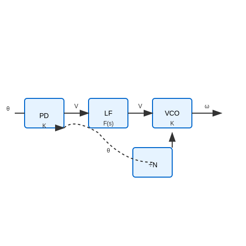
A phase-locked loop (PLL) is a feedback control system that synchronizes the phase and frequency of an output signal with a reference input signal. The fundamental architecture consists of four primary components: a phase detector (PD), a loop filter (LF), a voltage-controlled oscillator (VCO), and a feedback divider (optional, depending on application).
Phase Detector (PD)
The phase detector compares the phase difference between the reference signal θref and the feedback signal θfb, generating an error signal proportional to their phase difference. Common implementations include:
- Analog multipliers (e.g., Gilbert cell mixers) producing Verr = Kd sin(Δθ).
- Digital phase-frequency detectors (PFDs) with tri-state outputs for frequency acquisition.
Loop Filter (LF)
The loop filter shapes the error signal to stabilize the PLL dynamics. A second-order passive RC filter is typical, with transfer function:
where τ1 = R1C and τ2 = R2C. Active filters (e.g., charge pumps with integrators) are used in high-performance systems.
Voltage-Controlled Oscillator (VCO)
The VCO generates the output signal with frequency ωout proportional to the control voltage Vctrl:
where KVCO is the gain in rad/s/V. LC-tank or ring oscillators are common topologies, with trade-offs between phase noise and tuning range.
Feedback Divider (N)
In frequency synthesis applications, a divider with ratio N scales the VCO output to match the reference frequency:
Programmable counters or fractional-N dividers enable precise frequency steps. Delta-sigma modulation reduces fractional spurs.
System Dynamics
The linearized PLL model yields a closed-loop transfer function:
For a second-order system, the damping factor ζ and natural frequency ωn are:
Optimal values (ζ ≈ 0.707, ωn ≤ fref/10) balance lock time and stability.
1.2 Phase Detector Characteristics
Transfer Function and Linearity
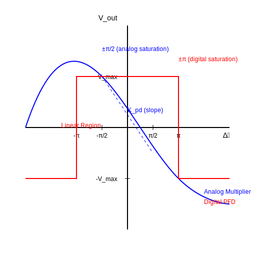
The phase detector (PD) in a PLL generates an output signal proportional to the phase difference between its two input signals. For an ideal linear phase detector, the output voltage Vout is given by:
where Kpd is the phase detector gain (in volts/radian) and Δϕ is the phase difference. Practical phase detectors exhibit nonlinearities outside a limited range, typically ±π/2 for analog multipliers and ±π for digital XOR-type detectors.
Common Phase Detector Types
Analog Multipliers (Mixer-Based)
When two sinusoidal signals V1 = A sin(ωt + ϕ1) and V2 = B sin(ωt + ϕ2) are multiplied:
Low-pass filtering removes the high-frequency component, leaving a DC term proportional to cos(Δϕ). For small phase differences (Δϕ ≪ 1), this approximates a linear response.
Digital Phase-Frequency Detectors (PFDs)
Modern PLLs commonly use sequential logic PFDs with the following characteristics:
- Linear range: ±2π radians
- Dead zone: Minimum phase difference required for response (typically < 100 ps)
- Frequency detection: Provides additional frequency discrimination capability
Noise and Spurious Performance
The phase detector's noise contribution is characterized by its phase noise floor and reference spurs. Key parameters include:
where Sϕ(f) is the phase noise power spectral density. Digital PFDs typically exhibit higher reference spurs due to periodic charge pump activity, requiring careful loop filter design.
Implementation Considerations
In CMOS implementations, the phase detector's:
- Propagation delay limits maximum operating frequency
- Mismatch between up/down paths creates static phase error
- Power supply rejection affects spur performance
Advanced designs use techniques like delay-matched buffers and differential charge pumps to mitigate these effects. For sub-picosecond jitter applications, superconducting Josephson junction phase detectors achieve unprecedented resolution below 10-6 radians.
1.3 Loop Filter Design Principles
Transfer Function and Stability Analysis
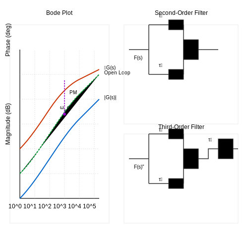
The loop filter in a phase-locked loop (PLL) shapes the system's closed-loop response, directly influencing stability, phase noise, and settling time. The most common loop filter configurations are passive and active, with the second-order passive RC filter being a standard choice. Its transfer function is given by:
where τ1 = R1C, τ2 = R2C, and τ3 represents higher-order poles if present. The open-loop gain G(s) of the PLL, including the VCO gain KVCO and phase detector gain KPD, is:
Stability is assessed via the phase margin (PM), which should typically exceed 45° for robust performance. The PM is derived from the open-loop transfer function's phase at the crossover frequency ωc, where |G(jωc)| = 1.
Noise Optimization and Bandwidth Trade-offs
Loop bandwidth (ωn) is a critical parameter balancing reference spur suppression and phase noise performance. A wider bandwidth reduces VCO phase noise contribution but increases susceptibility to reference noise. The optimal bandwidth is often derived from the noise-equivalent bandwidth (NEB):
where H(jω) is the closed-loop transfer function. For a second-order system with damping factor ζ, NEB simplifies to:
Practical designs often use ζ ≈ 0.707 (Butterworth response) to balance overshoot and settling time.
Higher-Order Filter Design
Third-order loops introduce an additional pole (τ3) to attenuate reference spurs. The transfer function becomes:
The added pole must be placed at least a decade above ωn to avoid degrading phase margin. Active filters with operational amplifiers are used when higher DC gain or charge-pump current matching is required. For example, a proportional-integral (PI) filter has the form:
Component Selection and Practical Considerations
Resistor thermal noise and capacitor dielectric absorption introduce non-idealities. Key design steps include:
- Capacitor selection: Use NP0/C0G ceramics for low leakage and minimal voltage coefficient.
- Resistor selection: Thin-film resistors exhibit lower noise than thick-film variants.
- Layout: Minimize parasitic capacitance to ground for high-frequency stability.
For charge-pump PLLs, the loop filter impedance at the reference frequency fref must be sufficiently low to suppress ripple voltage:
where ICP is the charge-pump current.
Voltage-Controlled Oscillator (VCO) Dynamics
Nonlinear Frequency Tuning and Gain Variations
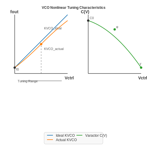
The output frequency fout of a VCO is ideally linear with respect to the control voltage Vctrl, expressed as:
where f0 is the free-running frequency and KVCO is the gain in Hz/V. In practice, KVCO exhibits nonlinearity due to semiconductor physics, parasitic capacitances, and temperature dependencies. For instance, in LC-tank VCOs, varactor diodes introduce a voltage-dependent capacitance C(V):
where C0 is the zero-bias capacitance, φ is the built-in potential, and γ is the grading coefficient. This nonlinearity causes KVCO to vary across the tuning range, leading to phase-locked loop (PLL) stability challenges.
Phase Noise and Jitter
VCO phase noise £(Δf) follows Leeson’s model, modified for modern CMOS designs:
Here, F is the noise factor, Q is the tank quality factor, and Δf1/f³ is the corner frequency of flicker noise upconversion. Jitter σt integrates phase noise across the offset frequencies:
Power Supply Rejection Ratio (PSRR)
VCOs are sensitive to supply noise, quantified by PSRR:
Differential topologies (e.g., cross-coupled LC oscillators) improve PSRR by 20–40 dB compared to single-ended designs. Techniques like regulated cascode biasing or on-chip decoupling capacitors further suppress supply-induced jitter.
Thermal and Aging Effects
Long-term frequency drift arises from thermal coefficients (e.g., TCf in ppm/°C) and aging mechanisms like hot-carrier injection. For a first-order approximation:
where A is a process-dependent constant, Ea is activation energy, and n is the time exponent. Compensation methods include temperature-stabilized bias circuits or digital calibration loops.
Practical Design Trade-offs
- Tuning range vs. phase noise: Wider tuning increases KVCO but degrades Q due to varactor losses.
- Supply voltage scaling: Lower VDD reduces power but exacerbates PSRR limitations.
- Process corners: Monte Carlo simulations are essential to bound fout and KVCO variations across PVT.
2. Fractional-N Frequency Synthesis
2.1 Fractional-N Frequency Synthesis
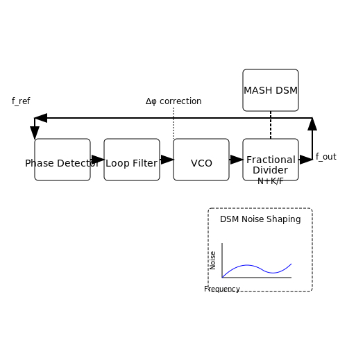
Fractional-N frequency synthesis overcomes the resolution limitations of integer-N PLLs by allowing non-integer division ratios. Instead of locking to a fixed multiple of the reference frequency, a fractional-N synthesizer dynamically modulates the divider value between two integers, achieving finer frequency steps without degrading phase noise performance.
Mathematical Basis
The output frequency of a fractional-N synthesizer is given by:
where N is the integer part of the division ratio, K is the fractional accumulator value, and F is the modulus of the fractional accumulator. For example, if N = 100, K = 3, and F = 8, the effective division ratio becomes 100.375.
Delta-Sigma Modulation
To suppress fractional spurs, modern implementations use delta-sigma modulation (DSM) to randomize the divider control sequence. A multi-stage noise shaping (MASH) DSM is commonly employed:
where ei represents quantization errors from previous stages. The MASH-1-1-1 architecture provides third-order noise shaping, pushing quantization noise to higher frequencies where it can be filtered by the PLL loop.
Phase Error Correction
Fractional division introduces deterministic phase errors that must be compensated. A common approach uses a digital-to-time converter (DTC) or charge pump current steering to inject corrective pulses:
Advanced implementations may employ adaptive calibration techniques to maintain sub-picosecond timing accuracy across process, voltage, and temperature variations.
Practical Implementation Challenges
- Spurious tones: Mismatches in phase correction circuitry can create fractional spurs at offsets of fref/F
- Quantization noise: Higher-order DSMs reduce in-band noise but increase high-frequency content that may alias back
- Loop bandwidth tradeoffs: Wider bandwidth helps suppress DSM noise but worsens reference feedthrough
Modern fractional-N synthesizers in RF applications routinely achieve <100 fs RMS jitter with channel spacing down to 1 Hz at GHz frequencies.
2.2 All-Digital PLL (ADPLL) Architectures
Core Principles of ADPLLs
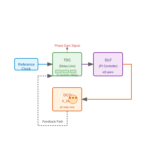
All-Digital Phase-Locked Loops (ADPLLs) replace analog components with digital equivalents, leveraging time-to-digital converters (TDCs), digital loop filters (DLFs), and digitally controlled oscillators (DCOs). The primary advantage lies in their scalability, noise immunity, and compatibility with modern CMOS processes. Unlike traditional PLLs, where loop dynamics are governed by continuous-time voltage-controlled oscillators (VCOs), ADPLLs operate in the discrete-time domain, enabling precise control through digital signal processing.
Time-to-Digital Converter (TDC) Design
The TDC quantizes the phase error between the reference clock and the DCO output. A common implementation uses a delay-line architecture, where the phase difference is measured by propagating the reference edge through a chain of inverters. The resolution of the TDC, given by the delay of a single inverter (Δt), directly impacts the ADPLL's jitter performance. For sub-picosecond resolution, vernier TDCs or noise-shaping techniques like ΔΣ modulation are employed.
where Tref is the reference clock period.
Digitally Controlled Oscillator (DCO)
The DCO replaces the analog VCO, with frequency tuning achieved through a digitally switched capacitor bank or current-starved inverter arrays. The frequency step size (Δf) is determined by the least significant bit (LSB) of the control word:
where KDCO is the gain (Hz/LSB) and D is the digital control word. Mismatch in capacitor arrays introduces nonlinearity, necessitating calibration algorithms.
Digital Loop Filter (DLF)
The DLF processes the TDC output, implementing proportional-integral (PI) control in the digital domain. Its transfer function in the z-domain is:
where α (proportional gain) and β (integral gain) are optimized for stability and lock time. Finite-word-length effects must be considered to avoid limit cycles.
Noise and Jitter Analysis
ADPLL phase noise stems from TDC quantization, DCO frequency steps, and clock jitter. The total output phase noise L(f) is dominated by the TDC at low offsets and the DCO at high offsets:
where SD(f) is the power spectral density of the DCO control noise.
Applications in Modern Systems
- Wireless transceivers: ADPLLs enable fast settling for frequency hopping in 5G NR and Wi-Fi 6.
- Clock generation: Used in microprocessors for low-jitter, multi-domain clock synthesis.
- Digital RF: Direct modulation of the DCO eliminates analog mixers in polar transmitters.
Advanced Techniques
Hybrid ADPLLs combine digital control with analog-assisted components (e.g., sub-sampling TDCs) to achieve femtosecond-level resolution. Adaptive bandwidth tuning dynamically adjusts α and β based on real-time noise measurements. For ultra-low power, event-driven ADPLLs bypass the reference clock, triggering updates only on phase errors.
2.3 Charge-Pump PLL Optimization
Charge-Pump Current Mismatch and Nonlinearity
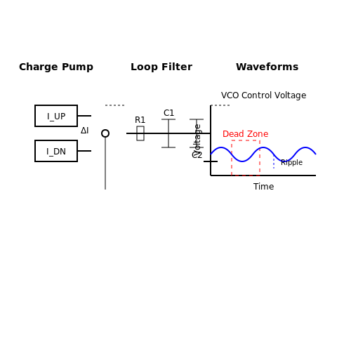
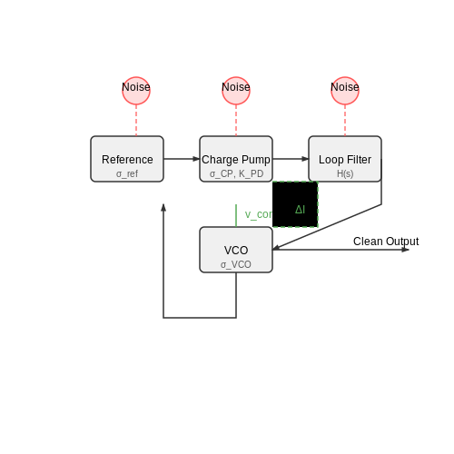
The charge-pump (CP) in a PLL is responsible for converting phase error into current pulses that drive the loop filter. A critical issue in CP-PLLs is current mismatch between the sourcing (IUP) and sinking (IDN) currents. Even a small mismatch introduces nonlinearity, leading to reference spurs and increased phase noise. The mismatch ratio is defined as:
For high-performance PLLs, ΔI must be kept below 1%. Techniques to mitigate mismatch include:
- Dummy switches to balance charge injection.
- Current mirror calibration using feedback loops.
- Dynamic element matching (DEM) to average out process variations.
Loop Filter Design Trade-offs
The loop filter converts charge-pump current into a control voltage for the VCO. A second-order passive RC filter is common, but its transfer function introduces trade-offs between stability and bandwidth:
Key optimization parameters include:
- Bandwidth (ωc): Must be ≤ 1/10th of the reference frequency to avoid aliasing.
- Phase margin: Typically targeted at 45°–60° for stability.
- Capacitor ratio: C2/C1 > 4 reduces ripple-induced jitter.
Dead Zone Elimination
When the phase error is near zero, the charge-pump may enter a dead zone, where neither the UP nor DN current is active. This results in increased jitter and poor tracking. Solutions include:
- Minimum pulse width circuits to force brief current pulses.
- Phase-frequency detector (PFD) reset delay tuning to prevent simultaneous turn-off.
- Offset current injection to keep the loop active near lock.
Noise Optimization Techniques
Charge-pump noise directly impacts PLL phase noise. The dominant sources are:
- Flicker (1/f) noise from current mirrors.
- Thermal noise from switches and resistors.
Noise reduction strategies include:
- Large-area transistors to minimize flicker noise.
- Differential charge-pump topologies to cancel common-mode noise.
- Switched-biasing to reduce thermal noise contributions.
Advanced Architectures: Fractional-N PLLs
In fractional-N PLLs, charge-pump linearity is even more critical due to ΣΔ modulation-induced noise shaping. A third-order loop filter is often used, with transfer function:
Key optimizations include:
- Noise cancellation via digital-to-time converters (DTCs).
- Adaptive bandwidth to balance lock time and phase noise.
- Multi-phase charge-pumps to reduce ripple.
2.4 Jitter Reduction Methods
Sources of Jitter in PLLs
Jitter in phase-locked loops (PLLs) arises from multiple sources, including:
- Phase noise in the voltage-controlled oscillator (VCO) – Intrinsic device noise and flicker noise contribute to random phase fluctuations.
- Supply and substrate noise coupling – Power supply variations modulate the VCO frequency.
- Reference clock jitter – The input reference signal may already contain timing uncertainty.
- Charge pump mismatches – Current source/sink imbalances introduce deterministic jitter.
The total jitter can be modeled as the root-sum-square (RSS) of these components:
Passive Filtering Techniques
Low-pass filtering the VCO control voltage reduces high-frequency noise components. A second-order passive loop filter with transfer function:
where \(\tau_z = R_1C_1\) and \(\tau_p = R_1C_1C_2/(C_1 + C_2)\), attenuates noise above the loop bandwidth. The optimal bandwidth balances reference noise rejection and VCO noise suppression.
Active Noise Cancellation
Feedforward techniques inject a compensating signal derived from supply noise measurements. For a supply noise \(v_{dd}(t)\), the correction voltage is:
where \(K_{VCO}\) is the VCO gain. This requires precise characterization of the supply sensitivity \(\partial f_{VCO}/\partial v_{dd}\).
Digital Calibration Methods
Background calibration continuously measures and corrects charge pump mismatches. A common approach uses a time-to-digital converter (TDC) to detect phase errors when the PLL is locked, then adjusts the pump currents:
The adaptation constant \(\alpha\) controls convergence speed versus steady-state ripple.
Layout Considerations
Physical implementation significantly impacts jitter performance:
- Differential VCO routing – Minimizes common-mode noise pickup.
- Guard rings – Isolate sensitive analog blocks from digital switching noise.
- Decoupling capacitors – Local high-frequency bypassing reduces supply impedance.
Advanced Architectures
Sub-sampling PLLs (SSPLLs) eliminate charge pump noise by directly sampling the VCO output. The sampling operation creates an inherent averaging effect, reducing jitter. The phase detection gain becomes:
independent of the charge pump current, improving supply rejection.
Injection-locked PLLs (ILPLLs) achieve ultra-low jitter by synchronizing to a clean reference pulse. The locking range must satisfy:
where \(I_{inj}\) is the injection current and \(V_{osc}\) the oscillation amplitude.
3. Phase Noise Modeling in PLLs
Phase Noise Modeling in PLLs
Phase noise in phase-locked loops (PLLs) arises from stochastic fluctuations in the oscillator output phase, degrading spectral purity and timing precision. Accurate modeling is critical for high-performance applications such as wireless communications, radar systems, and clock distribution networks.
Sources of Phase Noise
Phase noise originates from multiple mechanisms:
- Thermal noise (white noise): Introduces a flat noise floor proportional to kT/C.
- Flicker noise (1/f noise): Dominates at low offset frequencies due to active device imperfections.
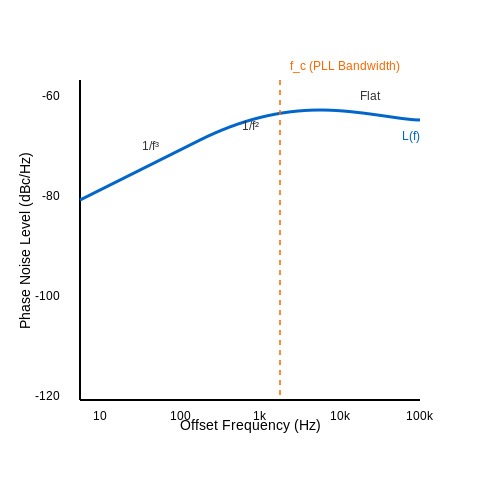
- VCO phase noise: Typically follows Leeson’s model, with regions defined by 1/f³, 1/f², and white noise.
- Reference oscillator noise: Propagates through the PLL, scaled by N² (division ratio).
Leeson’s Model for VCO Phase Noise
The modified Leeson equation describes single-sideband phase noise L(f):
where:
- F = noise factor of the active device,
- k = Boltzmann’s constant,
- T = temperature (Kelvin),
- Psig = oscillator signal power,
- f0 = carrier frequency,
- QL = loaded quality factor of the resonator,
- fc = flicker noise corner frequency.
PLL Phase Noise Transfer Functions
The PLL’s closed-loop response modulates noise contributions:
where H(f) is the loop filter transfer function. The contributions are:
- Reference noise (Lref): High-pass filtered by 1 - H(f).
- VCO noise (LVCO): Low-pass filtered by H(f).
- Divider noise (Ldiv): Behaves similarly to reference noise.
Noise Optimization Techniques
Key strategies include:
- Loop bandwidth tuning: Balancing VCO and reference noise suppression.
- High-Q resonators: Reducing 1/f² phase noise region slope.
- Active device biasing: Minimizing flicker noise via subthreshold operation or differential topologies.
3.2 Stability Criteria for Higher-Order Loops
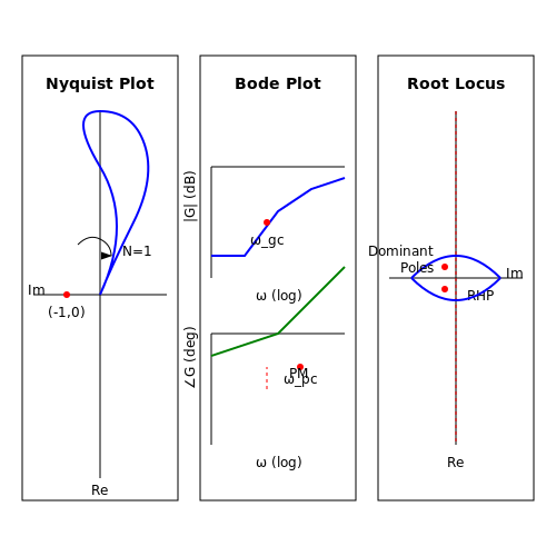
Higher-order phase-locked loops (PLLs) introduce additional poles and zeros, complicating stability analysis. Unlike second-order loops, where stability is primarily governed by damping factor (ζ) and natural frequency (ωn), third-order and higher systems require rigorous assessment via Nyquist, Bode, or root locus methods.
Open-Loop Transfer Function Analysis
The open-loop transfer function of an n-th order PLL is given by:
where Kd is the phase detector gain, Ko is the VCO gain, F(s) is the loop filter transfer function, and N is the number of integrators (order of the system). For a third-order loop with an active proportional-integral-derivative (PID) filter:
Nyquist Stability Criterion
The Nyquist criterion evaluates stability by analyzing encirclements of the critical point (−1, 0) in the complex plane. For a higher-order PLL:
- Plot G(jω)H(jω) for ω ∈ (0, ∞).
- Count the number of clockwise encirclements (N) of (−1, 0).
- The system is stable if N = P, where P is the number of open-loop poles in the right-half plane (RHP).
Bode Plot Stability Margins
Phase margin (ϕm) and gain margin (Gm) are critical metrics:
where ωgc is the gain crossover frequency (|GH| = 1) and ωpc is the phase crossover frequency (∠GH = −180°). For robust stability:
- Target ϕm > 45° and Gm > 6 dB.
- Higher-order loops often exhibit peaking in the phase noise transfer function if margins are insufficient.
Root Locus Method
The root locus plots closed-loop pole trajectories as loop gain K varies. For stability:
- No poles should migrate to the RHP for any K > 0.
- Dominant poles must remain sufficiently damped (ζ ≥ 0.5).
For a third-order PLL with a zero, the characteristic equation is:
Applying the Routh-Hurwitz criterion, the stability conditions are:
Practical Considerations
Higher-order loops are susceptible to:
- Parasitic poles from op-amp bandwidth or PCB parasitics.
- Nonlinearities in phase detectors or VCOs, invalidating linear models.
- Component tolerances, necessitating Monte Carlo analysis.
In frequency synthesizers, third-order loops are common to suppress reference spurs, but stability must be verified via simulation tools like SPICE or MATLAB.
3.3 Impact of Component Non-Idealities
Voltage-Controlled Oscillator (VCO) Phase Noise
The VCO's phase noise spectrum Sφ(f) deviates from the ideal Lorentzian distribution due to flicker (1/f) noise in active devices and thermal noise in varactors. For a bipolar VCO, the modified Leeson's equation becomes:
where fc is the flicker noise corner frequency (typically 10 kHz-1 MHz for CMOS). This results in close-in phase noise degradation by 10-20 dB/decade below fc.
Charge Pump Mismatch and Leakage
Non-ideal current sources in charge pumps exhibit:
- Current mismatch (ΔI): Causes reference spurs at fref with amplitude:
- Leakage currents (Ileak): Introduces static phase error Δφ = Ileak/ICP, degrading lock accuracy
Loop Filter Component Tolerances
5% tolerance in R and C components causes:
- ±10% variation in natural frequency ωn = √(KVCOICP/2πNC)
- ±15% damping factor ξ variation: ξ = (R/2)√(ICPKVCOC/2πN)
This results in underdamped (ξ < 0.5) or overdamped (ξ > 1.5) transient responses, with settling time variations up to 2× nominal.
Divider Timing Skew
Propagation delay mismatches Δt in multi-modulus dividers create periodic phase errors:
This manifests as spurious tones at ±1/Δt offsets from the carrier.
Substrate and Supply Coupling
In mixed-signal PLLs, digital switching noise modulates the VCO through:
- Substrate impedance (Zsub ≈ 50-200 Ω at GHz frequencies)
- Supply rejection ratio (PSRR < 20 dB above 100 MHz)
Resulting in sidebands at clock harmonics with amplitude:
Thermal Effects
Junction temperature fluctuations ΔT cause VCO frequency drift through:
where α ≈ -30 ppm/°C (CTAT) and β ≈ +0.5 ppm/°C² (PTAT) for typical LC-VCO designs.
3.4 Noise-Shaping Techniques
Noise-shaping is a critical method in phase-locked loop (PLL) design to mitigate phase noise and spurious tones by redistributing quantization noise to higher frequencies where it can be filtered out. This technique is particularly valuable in fractional-N PLLs, where delta-sigma modulation introduces high-frequency noise that must be managed.
Delta-Sigma Modulation in PLLs
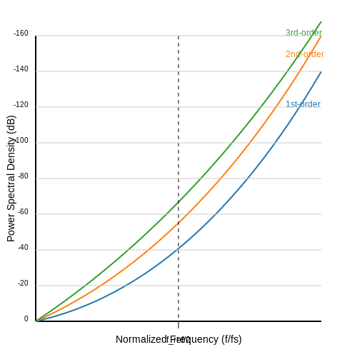
Delta-sigma modulators (DSMs) are widely used in fractional-N PLLs to achieve fine frequency resolution. A DSM shapes the quantization noise by pushing it to higher frequencies, allowing the PLL's low-pass characteristic to attenuate it. The noise transfer function (NTF) of an M-th order DSM is given by:
where M represents the modulator order. Higher-order modulators provide steeper noise shaping but introduce stability challenges.
High-Order Noise Shaping
Second and third-order DSMs are common in PLLs, but fourth-order designs are increasingly used for ultra-low phase noise applications. The power spectral density (PSD) of the shaped noise can be derived as:
where Δ is the frequency step size, fref is the reference frequency, and M is the DSM order. This equation shows the high-pass noise-shaping behavior, with noise suppression improving as M increases.
Stability Considerations
Higher-order DSMs risk instability due to excessive phase error accumulation. Multi-stage noise shaping (MASH) architectures, such as the MASH-1-1-1 or MASH-2-2, improve stability by cascading lower-order modulators. The output of an N-stage MASH DSM is:
where ek[n] represents the quantization error from the k-th stage. MASH modulators provide deterministic stability but require careful dithering to avoid spurious tones.
Dithering Techniques
Dithering injects pseudo-random noise to disrupt periodicity in the DSM output, reducing spurs. Common methods include:
- First-order dither: Adds white noise to the DSM input.
- High-pass dither: Shapes dither noise away from the PLL bandwidth.
- Sigma-dithered modulators: Combine dithering with noise shaping for optimal performance.
The effectiveness of dithering depends on the PLL's loop bandwidth and the DSM's noise transfer characteristics.
Practical Implementation
In modern PLLs, noise-shaping techniques are implemented using digital signal processing (DSP) blocks. Field-programmable gate arrays (FPGAs) and application-specific integrated circuits (ASICs) often integrate dedicated DSM cores with configurable order and dithering options. For example, a third-order MASH-1-1-1 DSM can achieve phase noise below −120 dBc/Hz at 1 MHz offset in a 28 nm CMOS process.
4. High-Speed Data Communication Systems
4.1 High-Speed Data Communication Systems
Phase-locked loops (PLLs) are critical in high-speed data communication systems, where precise clock synchronization and jitter reduction are paramount. In modern serial links operating at multi-gigabit rates, PLLs must compensate for channel impairments, including intersymbol interference (ISI), phase noise, and frequency drift.
Jitter and Phase Noise in High-Speed Links
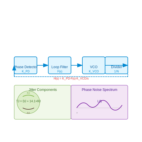
Jitter in high-speed systems is decomposed into random jitter (RJ) and deterministic jitter (DJ). RJ follows a Gaussian distribution and is primarily caused by thermal noise, while DJ includes periodic jitter (PJ) and data-dependent jitter (DDJ). The total jitter (TJ) at a bit error rate (BER) of 10−12 is given by:
Phase noise, represented in the frequency domain as L(f), is integrated to compute root-mean-square (RMS) jitter:
where f0 is the carrier frequency, and f1, f2 define the integration bandwidth.
Clock and Data Recovery (CDR) Architectures
High-speed CDR circuits employ PLL-based or delay-locked loop (DLL)-based topologies. A bang-bang CDR uses a binary phase detector for fast locking but suffers from higher jitter. In contrast, a linear phase detector offers better noise performance but requires precise calibration.
The loop dynamics of a PLL-based CDR are modeled by the transfer function:
where KPD is the phase detector gain, KVCO is the VCO gain, and F(s) represents the loop filter response.
Equalization and PLL Co-Design
In high-speed SerDes (Serializer/Deserializer) systems, feed-forward equalizers (FFEs) and decision-feedback equalizers (DFEs) mitigate ISI. The PLL bandwidth must be optimized to track low-frequency wander while rejecting high-frequency noise. A common trade-off is:
Adaptive PLLs with real-time bandwidth adjustment are increasingly used in standards like PCIe 6.0 and 112G PAM-4 interfaces.
Case Study: PLL in 56Gbps NRZ Systems
For a 56Gbps non-return-to-zero (NRZ) link, a typical PLL employs a LC-tank VCO with a phase noise of −110 dBc/Hz at 1 MHz offset. The reference clock’s phase noise must be below −150 dBc/Hz to avoid dominating the total jitter budget. The loop filter is often a 3rd-order active design to suppress reference spurs.
4.2 Clock Generation for Microprocessors
Phase-Locked Loop (PLL) Architectures for Clock Synthesis
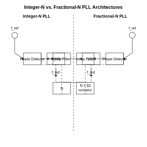
Modern microprocessors demand low-jitter, high-frequency clock signals with precise synchronization. Integer-N and fractional-N PLLs dominate clock generation, each with distinct trade-offs. Integer-N architectures use a fixed feedback divider (N), producing an output frequency fout = N · fref. While simple, their frequency resolution is limited to fref, necessitating lower reference frequencies for fine steps—at the cost of increased phase noise.
Fractional-N PLLs overcome this by dynamically modulating the divider ratio. A delta-sigma modulator dithers between integer values (e.g., N and N+1), achieving an effective fractional divide ratio N + α, where α is the fractional part. This enables higher reference frequencies without sacrificing resolution:
Jitter Reduction Techniques
Clock jitter directly impacts microprocessor timing margins. Key mitigation strategies include:
- Low-noise voltage-controlled oscillators (VCOs): Ring oscillators offer wide tuning ranges but higher phase noise; LC-tank VCOs provide superior noise performance at the expense of area.
- Sub-sampling phase detection (SSPD): Reduces charge pump noise by sampling the VCO output directly, minimizing linear-region noise contributions.
- Digital PLLs (DPLLs): Leverage time-to-digital converters (TDCs) and digital loop filters for noise shaping and process scalability.
Spread-Spectrum Clocking
To mitigate electromagnetic interference (EMI), spread-spectrum techniques modulate the output frequency with a low-frequency profile (e.g., triangular or Hershey-kiss). This spreads energy across a bandwidth Δf, reducing peak emissions. The modulation index m is constrained by processor timing constraints:
Case Study: x86 Clock Generation
Intel’s processors employ a multi-PLL hierarchy: a central fractional-N PLL generates the core clock, while distributed integer-N PLLs derive memory and I/O clocks. Deskew circuits align edges using delay-locked loops (DLLs), ensuring sub-10 ps synchronization. The core PLL achieves < 0.5 ps RMS jitter at 5 GHz through LC-VCOs and 3rd-order delta-sigma modulation.
Power Supply Noise Rejection
Power delivery network (PDN) noise couples into VCOs, inducing jitter. Differential VCO topologies and regulated supply cascodes improve PSRR. For example, a complementary NMOS-PMOS VCO with tail current filtering achieves > 40 dB rejection at 100 MHz switching noise frequencies.
Wireless Transceiver Design
Phase-Locked Loops in RF Transceivers
Phase-locked loops (PLLs) are fundamental to modern wireless transceivers, providing stable frequency synthesis, clock recovery, and modulation/demodulation. In RF systems, PLLs must achieve low phase noise, fast locking, and high spectral purity to meet stringent communication standards such as 5G NR, Wi-Fi 6, and Bluetooth Low Energy (BLE). The primary challenges include minimizing jitter in high-frequency oscillators and ensuring robust operation under varying environmental conditions.
where N is the division ratio of the feedback path and fref is the reference frequency. The loop bandwidth (ωc) must be optimized to balance between noise suppression and transient response:
where KVCO is the VCO gain, KPD is the phase detector gain, and τ is the loop filter time constant.
Fractional-N Synthesis for Wideband Operation
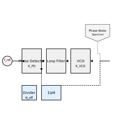
Traditional integer-N PLLs suffer from limited frequency resolution and high phase noise when used in wideband systems. Fractional-N synthesis overcomes this by dynamically modulating the division ratio N using a sigma-delta modulator (ΣΔM). The effective division ratio becomes:
where k is the fractional accumulator value and m is the modulator bit depth. This technique enables fine frequency steps (Δf) given by:
However, ΣΔ quantization noise must be suppressed using high-order loop filters or digital pre-distortion techniques.
Jitter and Phase Noise Optimization
In wireless transceivers, phase noise directly impacts error vector magnitude (EVM) and bit error rate (BER). The Leeson-Cutler equation models phase noise (£(Δf)) in oscillators:
where F is the noise factor, Q is the resonator quality factor, and Δf1/f³ is the flicker noise corner. Techniques to minimize phase noise include:
- Using high-Q LC tanks or BAW resonators.
- Implementing sub-sampling PLLs to reduce reference noise.
- Applying injection-locking for coupled oscillators.
Digital PLLs for Software-Defined Radios
Digital PLLs (DPLLs) replace analog components with time-to-digital converters (TDCs) and digital loop filters, enabling software-defined configurability. A second-order DPLL has a loop filter transfer function:
where α and β are proportional and integral gains, respectively. DPLLs excel in multi-standard radios, allowing dynamic reconfiguration of bandwidth and damping factor via firmware updates.
Case Study: 5G mmWave PLL Design
In 5G mmWave transceivers (e.g., 28 GHz bands), PLLs must achieve sub-100 fs RMS jitter while operating at multi-GHz frequencies. A common architecture employs:
- A 10 MHz reference clock derived from a temperature-compensated crystal oscillator (TCXO).
- A 4th-order ΣΔ fractional-N synthesizer with a 40 nm CMOS VCO.
- An adaptive bandwidth loop filter to optimize for both acquisition and tracking modes.
Measured results in such designs typically show phase noise below -110 dBc/Hz at 1 MHz offset.
Radar and Satellite Systems
Phase-Locked Loops in Radar Systems
In modern radar systems, phase-locked loops (PLLs) are critical for generating stable local oscillator (LO) signals and performing coherent demodulation of received echoes. The PLL ensures phase coherence between transmitted and received signals, enabling precise Doppler shift measurement and target velocity estimation. A radar PLL typically operates at microwave frequencies, requiring low phase noise to maintain detection sensitivity.
The loop bandwidth must be optimized to track Doppler shifts while rejecting phase jitter. For a pulsed radar system with pulse repetition frequency (PRF) fp, the PLL bandwidth BL should satisfy:
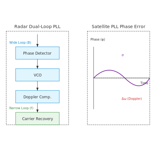
to avoid inter-pulse phase disturbances. Advanced techniques like dual-loop PLLs combine wide and narrow bandwidth loops to achieve both fast acquisition and low-noise tracking.
Satellite Communication PLL Architectures
In satellite transponders, PLLs perform carrier recovery and frequency synthesis with extreme stability. The unique challenges include:
- Compensating for Doppler shifts up to ±40 kHz in LEO systems
- Maintaining phase coherence across long propagation delays
- Operating in high-radiation environments requiring radiation-hardened designs
The phase error variance σφ2 for a satellite PLL is given by:
where Pc is carrier power, N0 is noise density, and Δω is the frequency offset. This leads to the implementation of Kalman filter-enhanced PLLs that dynamically adjust loop parameters based on signal conditions.
High-Orbit vs Low-Orbit System Requirements
Geostationary systems emphasize ultra-low phase noise (< -100 dBc/Hz at 1 kHz offset) due to their high symbol-rate QPSK/8PSK modulations. Low-Earth orbit constellations require rapid frequency hopping capabilities, with PLL settling times under 50 μs being common for TDMA systems.
The Allan deviation σy(τ) provides a key metric for oscillator stability:
where fi are frequency measurements averaged over interval τ. Advanced rubidium or hydrogen maser references achieve σy below 10-13 for τ = 1000s in deep-space applications.
Modern Implementation Techniques
Current systems employ:
- Fractional-N synthesizers with ΔΣ dithering for < 0.01 Hz resolution
- Optical PLLs using optical phase detectors for THz carrier generation
- Digital PLL (DPLL) architectures with adaptive bandwidth control
The DPLL phase detector characteristic is implemented as:
where I[n] and Q[n] are the in-phase and quadrature samples. This digital approach enables nonlinear tracking algorithms impossible in analog implementations.
5. Key Research Papers on PLL Techniques
5.1 Key Research Papers on PLL Techniques
- ISSCC Highlights: Advances in PLLs | DigiKey - Digi-Key Electronics — One ISSCC paper described a 2.9- to 4.0-GHz fractional-N digital PLL based on a TDC that achieved a jitter of 560 fs rms (from 3 kHz to 30 MHz) at 4.5-mW power consumption. The circuit synthesizes frequencies between 2.92 and 4.05 GHz with 70-Hz resolution. (Paper 5.1, ISSCC 2011)
- Design of an advanced PLL for accurate phase angle extraction under ... — locked loop (PLL) algorithm [6-10]. This paper considers the second category, in which a PLL is used as the main component for enabling the implementation of the control scheme. The phase angle extraction of PLL is, however, affected by various abnormal grid scenarios such as unbalanced grid faults, harmonic distortion,
- PDF Isscc 2011 / Session 15 / High-performance S Ocs & Components / 15 — phase-locked loop (PLL) [4], or in the clock tree while the clock edge is propa-gating [5,6]. A brief analysis of the adaptive clocking scheme is shown in Fig. 15.5.1 (bottom left). The four waveforms represent the supply voltage with res-onant noise, and the clock period modulation effect seen by the PLL, the clock
- Design of an advanced PLL for accurate phase angle extraction under grid voltage HIHs and DC offset — Therefore, there is a need to develop more advanced and suitable PLL techniques that can work efficiently under these off-nominal grid situations. The work presented in this paper mainly focuses on the mitigation of harmonics/interharmonics (HIHs) and DC offset (DO) problems. ... The presence of non-linear power electronic and DC loads together ...
- PDF Design Techniques of Energy E cient PLL for Enhanced Noise and Lock ... — PLL to o er superior performance is the prime objective of this research. It is desirable for the PLL to have fast locking, low noise, low reference spur, wide lock range, low power consumption consuming less silicon area. To achieve these performance parameters simultaneously in a PLL being a challenging task is taken up as a scope of the ...
- (PDF) Design and Implementation of Digital PLL using Self Correcting ... — The phase-locked loop (PLL) is one of the key building blocks of modern electronic designs. This paper presents a novel PLL structure that utilizes a "flying-adder" frequency synthesizer as its digital control oscillator (DCO), a software implemented adaptive IIR filter as its loop filter, and a unique counter as its phase detector.
- PDF Design and Analysis of Efficient Phase Locked Loop for Fast Phase and ... — A PLL is capable of tracking the phase changes that falls in this bandwidth of the PLL. A PLL also multiplies a low-frequency reference clock CK ref to produce a high-frequency clock CK out this is known as clock synthesis. A PLL has a negative feedback control system circuit. The main objective of a PLL is to generate a signal
- Design of a high‐performance advanced phase locked loop with high ... — The supply noise is decreased by three reference clock cycles and the effect is that the measurement of jitter is better. Advanced Phase Locked Loop oscillates at frequencies ranging from 500 MHz to 4 GHz. A root mean square jitter of 1.29 ps is observed at 1 GHz. Our PLL is rated at 92.1-μW, with power used at 0.31 mW/GHz.
- (PDF) Phase-locked loop techniques - A survey - ResearchGate — Phase-locked loop (PLL) is a technique which has contributed significantly toward the technology advancement in communication and motor servo control systems in the past 30 years.
- A new programmable low noise all digital phase-locked loop architecture — studied and documented in countless journal papers, books, and articles. In fact there exists so much information about PLL's it can be overwhelming and difficult to isolate the specific
5.2 Recommended Books on PLL Design
- Phase-locked loops (Chapter 5) - Analogue Electronic Circuits and Systems — Computer aided circuit design. Appendices. 5 - Phase-locked loops. Published online by Cambridge University Press: 05 June 2012 ... The PLL contains a phase detector, a low-pass filter and a voltage-controlled oscillator in an arrangement as shown in Fig. 5.2. ... Book: Analogue Electronic Circuits and Systems; Online publication: 05 June 2012 ...
- Power Management Techniques for Integrated Circuit Design — available in electronic books. ... 4.3 Design Techniques When Using MLCC with a Small Value of RESR 201 ... 5.2.3 Technique of PLL Modulator 302 5.2.4 Full Analysis of Frequency Variation under Different v IN,v OUT, and i Load 304 5.2.5 Adaptive On-Time Controller for Pseudo-Constant f
- Phase Locked Loops Design Simulation and Applications by R BEST — PROFESSIONAL CD-ROM of new software for the design of entire PLL systems up to order 5 'Step-by-step procedures for design of linear and digital PLL circuits 'Simple method for designing higher-order PLL systems Ready-to-use design examples for digital PLL frequency synthesizers New directory of commercially available PLL IC's FIFTH EDITION Phase-Locked Loops DESIGN, SIMULATION, AND ...
- PDF Analysis and Design CMOS PLL Synthesizers: — design criteria for low distortion in feedback opamp circuite hernes & saether isbn: 1-4020-7356-9 circuit techniques for low-voltage and high-speed aid converters walteri isbn: 1-4020-7244-9 design of high-performance cmos voltage controlled oscillators dai and hajani isbn: 1-4020-7238-4 cmos circuit design for rf sensors gudnason and bruun
- Analog - PLL Performance, Simulation, and Design 4th — This document is the fourth edition of the book "PLL Performance, Simulation, and Design" by Dean Banerjee. It contains 19 chapters that cover topics related to phase locked loops (PLLs) including basics, performance and simulation, and design. The preface explains that the book takes a rigorous mathematical approach to derive PLL formulas and compares them to measured data. It has been ...
- PDF PLL Performance, Simulation, and Design 4 Edition - E2E™ 设计支持 — FM modulated signal. Although these are legitimate applications of the PLL, the primary ocus of this book is the use of a PLL as a frequency synthesizer. In this type of application, the PLL is used to generate a set of discrete frequencies. A good example of this is FM radio. In FM radio, the valid stations range from 88 to 108 MHz, and
- PDF PLL Performance, Simulation, and Design - 德州仪器 TI.com.cn — grow in PLL knowledge this way. knowing what a result should theoretically be, it By makes it easier to spot and diagnose problems with a PLL circuit. This book takes a unique approach to PLL design by combining rigorous mathematical derivations for formulas with actual measured data. When there is agreement between these two, then one can feel ...
- PDF Design of CMOS Phase-Locked Loops - Cambridge University Press & Assessment — oscillator design, covering fundamentals to advanced topo logies; and extensive use of circuit simulations to teach design mentality, highlight design aws, and connect theory with practice. Offering over 200 thought-provoking examples that demonstrate best practices and com mon pitfalls, 250 end-of-chapter homework
- Phase-Locked Loops: System Perspectives and Circuit Design Aspects — Phase-Locked Loops Discover the essential materials for phase-locked loop circuit design, from fundamentals to practical design aspects A phase-locked loop (PLL) is a type of circuit with a range of important applications in telecommunications and computing. It generates an output signal with a controlled relationship to an input signal, such as an oscillator which matches the phases of input ...
- Behzad Razavi - Design of CMOS Phase-Locked Loops - Scribd — Design of CMOS Phase-Locked Loops. Using a modern, pedagogical approach, this textbook gives students and engineers a comprehensive and rigorous knowledge of CMOS PLL design for a wide range of applications. It features intuitive presen-tation of theoretical concepts, built up gradually from their simplest form to more practical systems; broad coverage of key topics, including oscillators ...
5.3 Online Resources and Tutorials
- PDF Clocking and PLL User Guide: Agilex 5 FPGAs and SoCs — Explore more resources ... Clocking and PLL User Guide: Agilex™ 5 FPGAs and SoCs Updated for Quartus® Prime Design Suite: 24.3 Online Version Send Feedback 813671 2025.01.24. Explore more resourcesAltera\256 Design Hub. ... 5.2.4. IOPLL IP Core Parameters - Advanced Parameters Tab.....38 5.3. IOPLL IP Core Ports and Signals.....39 . Contents ...
- 3. Agilex™ 5 Clocking and PLL Design Considerations - Intel — 1. Agilex™ 5 Clocking and PLL Overview 2. Agilex™ 5 Clocking and PLL Architecture and Features 3. Agilex™ 5 Clocking and PLL Design Considerations 4. Clock Control Intel® FPGA IP Core 5. IOPLL Intel® FPGA IP Core 6. I/O PLL Reconfiguration 7. Document Revision History for the Clocking and PLL User Guide: Agilex™ 5 FPGAs and SoCs
- PDF Contents — 5.3 Analog PLL Circuits 5 5.4 Analog PLL Components 9 5.5 Analog PLL Circuit Drawbacks 18 5.6 Digital PLLs 19 5.7 Conclusion 26 Bibliography 29. MITPress NewMath.cls LATEX Book Style Size: 6x9 December 7, 2020 12:44am. MITPress NewMath.cls LATEX Book Style Size: 6x9 December 7, 2020 12:44am 5 Phase-Locked Loops
- A 5.3GHz digital-to-time-converter-based fractional-N all-digital PLL ... — Advanced deep-submicron CMOS processes are well-suited for a digital implementation of phase-locked loop-(PLL) based frequency synthesizers. Recently, several RF all-digital phase-locked loops (ADPLL) have been reported. While ADPLLs come close to achieving the phase-noise performance of analog PLLs, the in-band spur level requirement is still challenging. In this paper we present a new ...
- PDF A Digital PLL with Multi-tap LMS-based Bandwidth Control - polimi.it — tap adaptive filtering. The method requires no injection of a training sequence, potentially degrading phase noise, and it is particularly suitable for bang-bang PLLs whose loop bandwidth depends on input noise. A 3.7-to-4.1-GHz PLL prototype embedding a 16-tap adaptive filter for loop gain estimation demonstrates 150-kHz loop bandwidth over ...
- Advanced Frequency Synthesis Techniques Using All-Digital ... - Springer — Over the past two decades, all-digital techniques for RF frequency synthesis have gained significant interest. In this chapter, we will review the all-digital phase-locked loop (ADPLL) architecture (also known as the phase-domain ADPLL and retrospectively classified as the counter-based ADPLL) followed by new techniques that help push the jitter performance.
- PDF Design of CMOS Phase-Locked Loops - Cambridge University Press & Assessment — cy dividers; tutorial chapters on high-performance oscillator design, covering fundamentals to advanced topo logies; and extensive use of circuit simulations to teach design mentality, highlight design aws, and connect theory with practice. Offering over 200 thought-provoking examples that demonstrate best practices and com
- PDF Practical Tips for Phase- Locked Loop Design - IEEE — • PLL acts as a low-pass filter with respect to the reference modulation. High-frequency reference jitter is rejected • Low-frequency reference modulation (e.g., spread-spectrum clocking) is passed to the VCO clock • PLL acts as a high-pass filter with respect to VCO jitter • "Bandwidth" is the modulation frequency at which the PLL
- PDF Tutorial on Digital Phase-Locked Loops - CppSim — M.H. Perrott 2 Why Are Digital Phase-Locked Loops Interesting? Performance is important-Phase noise can limit wireless transceiver performance-Jitter can be a problem for digital processors The standard analog PLL implementation is problematic in many applications-Analog building blocks on a mostly digital chip pose - design and verification challenges
- PDF Phase-Locked Loops: A Control Centric Tutorial — The most basic block diagram of a PLL is shown in Figure 1. This diagram shows the components that every PLL must have, namely: • A phase detector (PD). This is a nonlinear device whose output contains the phase difference between the two oscillating input signals. • A voltage controlled oscillator (VCO). This is an-
5.4 Advanced Topics for Further Study
- Level 5 Advanced Technician Diploma in Electrical and Electronic ... — and Electronic Engineering learners must achieve the 2 mandatory units and a minimum of 6 optional units. City & Guilds unit number/UAN. Unit title. GLH. NLH. Unit 501 R/506/9276. Advanced mathematics for electrical and electronic engineering. 85. 200. Unit 502 D/506/9278. Electrical and electronic 91 engineering principles. 200. Unit 503 Y/506 ...
- PDF Contents — MITPress NewMath.cls LATEX Book Style Size: 6x9 December 7, 2020 12:44am Contents 5 Phase-Locked Loops 1 5.1 Overview 2 5.2 Introduction 2 5.3 Analog PLL Circuits 5 5.4 Analog PLL Components 9 5.5 Analog PLL Circuit Drawbacks 18
- PDF Adaptive PLL Architecture Combining High Spectral Purity and Fast ... — 164 Adaptive PLL Architecture For higher values of phase margin than 53°, a dominant real pole moves to the right on the real axis, towards the zero at which lies at a relatively low frequency. This pole is responsible for the slowing down of the PLLresponse for values of as seen in Figure 5-4. Figure 5-5 shows that the
- PDF FREQUENCY ACQUISITION TECHNIQUES FOR PHASE LOCKED LOOPS - iczhiku.com — 2.1 What is a PLL?, 3 2.2 Second-Order PLL, 7 2.3 Second-Order PLL Type One, 7 2.4 Second-Order PLL Type Two, 7 2.5 Higher-Order PLL's, 8 2.6 Disturbances, 8 2.7 Frequency Steering and Capture, 9 2.8 Effect of DC Offsets or Noise Prior to the Loop Filter, 10 2.9 Injection-Locked Oscillations, 15 3 Simulating the PLL Linear Operation Mode 17
- Analog - PLL Performance, Simulation, and Design 4th — This document is the fourth edition of the book "PLL Performance, Simulation, and Design" by Dean Banerjee. It contains 19 chapters that cover topics related to phase locked loops (PLLs) including basics, performance and simulation, and design. The preface explains that the book takes a rigorous mathematical approach to derive PLL formulas and compares them to measured data. It has been ...
- PDF Design of CMOS Phase-Locked Loops - Cambridge University Press & Assessment — rigorous knowledge of CMOS PLL design for a wide range of appl ications. It features intuitive presen-tation of theoretical concepts, built up gradually from the ir simplest form to more practical systems; broad coverage of key topics, including oscillators, phase noise, analog PLLs, digital PLLs, RF synthesizers, delay-
- PDF CMOS Phase-Locked-Loop Applications (Rev. B) - Texas Instruments — the basic loop operation is included as an introduction to phase-lock techniques. Complete circuit designs, with and without a frequency-divide ratio, are included as examples. Examples also are given of various filters operating over a range of frequencies. Basic Loop Operation The HC/HCT4046A PLL with VCO is a high-speed CMOS IC designed for ...
- PDF pll project report - National Institute of Technology, Rourkela — Phase locked loop (PLL) [1-3] is the heart of the many modern electronics as well as communication system. Recently plenty of the researches have conducted on the design of phase locked loop (PLL) circuit and still research is going on this topic. Most of the researches have
- PDF Phase-locked Loops for Wireless Communications — Also included are some techniques to analytically estimate the phase noise of a divider before it is even fabricated. In the past year, many students in the short courses have been asking for design help on optical phase-locked loops. A new chapter has been added on this topic. Because many designers will be new to optical communications, I
- PDF 3.1. Introduction to All- Digital PLL - Seoul National University — Integrated Systems Design Laboratory, SNU D.K.Jeong Advantages of ADPLL • No analog tuning voltage - Suitable for deep-submicron tech using low supply voltage • PVT variation can be compensated more easily - Stable transfer characteristic • Digital filter - Passive components are not necessary - Less sensitive to gate leakage - Easily benefit from technology shrink