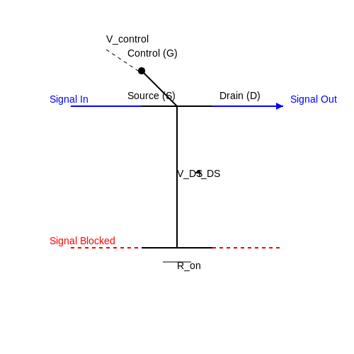
Voltage Controlled Oscillators
1. Definition and Basic Operating Principle
Voltage Controlled Oscillators: Definition and Basic Operating Principle
Fundamental Definition
A Voltage Controlled Oscillator (VCO) is an electronic circuit that generates a periodic signal whose frequency is directly controlled by an input voltage. Unlike fixed-frequency oscillators, VCOs exhibit a linear or nonlinear relationship between the control voltage Vctrl and the output frequency fout, expressed as:
where f0 is the center frequency when Vctrl = 0, and KVCO (expressed in Hz/V) is the voltage-to-frequency gain or tuning sensitivity.
Core Operating Principle
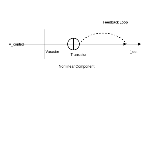
The VCO's operation relies on a voltage-dependent reactance element, typically implemented using:
- Varactor diodes (voltage-variable capacitance)
- Transconductance amplifiers (in relaxation oscillators)
- Voltage-controlled current sources (in ring oscillators)
For a LC-tank VCO, the oscillation frequency is governed by:
where C(Vctrl) is the varactor's voltage-dependent capacitance. The tuning curve is nonlinear due to the square root dependence, requiring linearization techniques in precision applications.
Phase-Locked Loop Context
In Phase-Locked Loops (PLLs), VCOs serve as the frequency-generating element. The open-loop transfer function reveals the VCO's integral relationship between phase and control voltage:
This property makes VCOs inherently unstable in open-loop operation but ideal for closed-loop frequency synthesis.
Key Performance Metrics
| Parameter | Definition | Typical Range |
|---|---|---|
| Tuning Range | Frequency span across control voltage limits | 10%–200% of f0 |
| Phase Noise | Short-term frequency stability | -80 to -160 dBc/Hz @ 1MHz offset |
| Pushing/Pulling | Sensitivity to supply/load variations | 1–100 MHz/V |
Practical Implementations
Modern VCO architectures include:
- Cross-coupled LC oscillators (low phase noise)
- Ring oscillators (wide tuning, compact layout)
- Crystal-based VCOs (high stability)
For example, a Colpitts VCO using a BJT and varactor diode achieves phase noise below -120 dBc/Hz at 100 kHz offset through careful Q-factor optimization of the tank circuit.
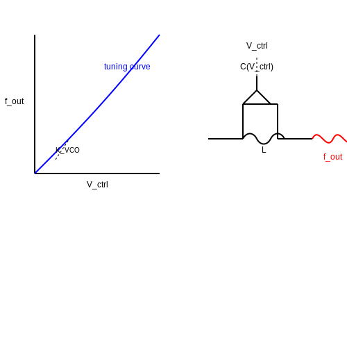
1.2 Key Parameters: Frequency Range, Tuning Sensitivity, and Linearity
Frequency Range
The frequency range of a VCO defines the minimum and maximum oscillation frequencies achievable under specified operating conditions. Mathematically, it is expressed as:
where fmax and fmin are determined by the resonator design and active device limitations. In LC-tank VCOs, the range is fundamentally constrained by:
Practical implementations often achieve octave tuning ranges (2:1 ratio) through varactor diodes with capacitance ratios (Cmax/Cmin) exceeding 3:1. Extended ranges require switched capacitor banks or multi-resonator architectures.
Tuning Sensitivity (KVCO)
The tuning sensitivity, denoted KVCO, quantifies the frequency change per unit control voltage (typically in MHz/V):
For a varactor-tuned LC oscillator, this derives from the voltage-dependent capacitance C(V):
High KVCO improves frequency resolution in phase-locked loops but increases susceptibility to control voltage noise. Typical values range from 10 MHz/V for precision applications to 100 MHz/V for wideband systems.
Linearity
VCO linearity describes the deviation from ideal frequency-versus-control-voltage characteristics. Nonlinearity introduces spurious tones and complicates loop dynamics in PLLs. The normalized nonlinearity coefficient α is defined as:
Three dominant sources contribute:
- Varactor nonlinearity: Arising from the C-V curve's hyperbolic nature in abrupt junction diodes
- AM-to-FM conversion: Amplitude variations modulating the effective capacitance
- Supply pushing: Frequency dependence on power rail fluctuations
Advanced techniques like differential varactor pairs and constant-amplitude biasing can achieve α < 0.1% across octave ranges. Digital predistortion in synthesizers further compensates residual nonlinearities.
Parameter Interdependence
The three parameters exhibit fundamental trade-offs:
- Wider frequency ranges typically degrade KVCO consistency and linearity
- High tuning sensitivity amplifies supply noise and reference spurs
- Linearity improvements often come at the cost of reduced tuning range
Modern VCO designs employ composite approaches - such as dual-path control (coarse/fine tuning) or digital assist techniques - to circumvent these limitations in high-performance RF systems.
1.3 Types of VCOs: Analog vs. Digital
Analog Voltage-Controlled Oscillators
Analog VCOs generate continuous sinusoidal, triangular, or sawtooth waveforms by leveraging voltage-dependent reactance elements, typically varactor diodes or voltage-controlled capacitors. The oscillation frequency f follows the governing equation:
where L is the inductance and C(V) is the voltage-dependent capacitance. Analog VCOs exhibit superior phase noise performance due to their continuous tuning nature, making them indispensable in RF applications such as phase-locked loops (PLLs) and frequency synthesizers. However, they suffer from temperature drift and nonlinearity in the control voltage-to-frequency response.
Digital Voltage-Controlled Oscillators
Digital VCOs employ numerically controlled oscillators (NCOs) or direct digital synthesis (DDS) techniques to generate discrete waveforms. The output frequency is determined by:
where M is the tuning word, fclk is the reference clock frequency, and N is the phase accumulator bit width. Digital VCOs offer precise frequency control, rapid switching, and immunity to analog drift effects. However, they introduce quantization noise and require high-speed digital-to-analog converters (DACs) for smooth waveform reconstruction.
Key Performance Trade-offs
- Phase Noise: Analog VCOs typically achieve better close-in phase noise due to continuous tuning, while digital VCOs exhibit higher noise floors from clock jitter and quantization.
- Linearity: Digital VCOs provide superior linearity in the control voltage-to-frequency transfer function, whereas analog variants require calibration to mitigate nonlinearities.
- Power Consumption: Analog designs often consume less power at high frequencies, while digital implementations scale efficiently with CMOS technology nodes.
Hybrid Architectures
Modern systems frequently combine analog and digital techniques, such as using a digital loop filter in an analog PLL or employing a delta-sigma modulator to enhance the resolution of a digital VCO. These hybrid approaches optimize the trade-offs between phase noise, power, and tuning range.
2. Voltage-to-Frequency Conversion Mechanisms
2.1 Voltage-to-Frequency Conversion Mechanisms
Core Principles of Voltage-to-Frequency Conversion
The fundamental mechanism of a voltage-controlled oscillator (VCO) relies on converting an input control voltage into a corresponding output frequency. This conversion is governed by the relationship:
where fout is the output frequency, KVCO is the VCO gain (in Hz/V), Vin is the input control voltage, and f0 is the center frequency when Vin = 0. The linearity of this relationship depends on the implementation technique.
Varactor-Based Tuning
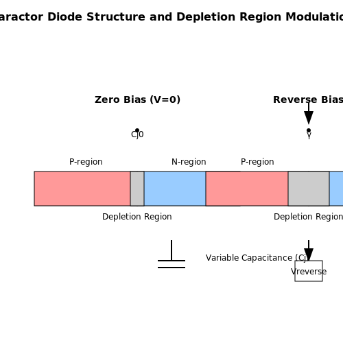
In LC-tank VCOs, frequency tuning is typically achieved through varactor diodes. The capacitance of a reverse-biased varactor varies with applied voltage:
where Cj0 is the zero-bias junction capacitance, φ is the built-in potential, and γ is the grading coefficient (0.5 for abrupt junctions, 0.33 for graded). This capacitance variation modifies the LC tank's resonant frequency:
Current-Starved Inverter Approach
In ring oscillator VCOs, voltage-to-frequency conversion occurs by controlling the charging current of delay stages. For an N-stage current-starved inverter:
where Ictrl is the control current (proportional to Vin), Cload is the nodal capacitance, and Vswing is the output voltage swing. The linearity is maintained when transistors operate in saturation.
Transconductance-Based Conversion
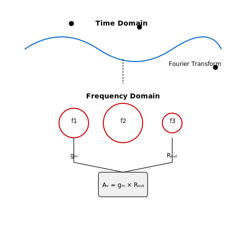
Some VCO architectures employ transconductance (gm) stages where:
By designing gm to be linearly dependent on Vin, the output frequency becomes directly proportional to the input voltage. This approach is common in OTA-based relaxation oscillators.
Nonlinearity Considerations
Practical VCOs exhibit nonlinearities due to:
- Varactor capacitance-voltage nonlinearity
- MOSFET velocity saturation in current mirrors
- Supply voltage variations affecting gm
These can be mitigated through:
- Predistortion techniques
- Differential control voltage topologies
- Calibration loops in digital PLL implementations
Thermal and Process Variations
The voltage-to-frequency relationship is affected by temperature-dependent parameters:
Process variations introduce additional spread, typically requiring trimming or automatic frequency calibration in modern IC implementations.
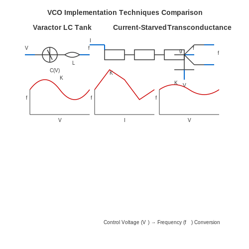
2.2 Resonator Types: LC Tanks, Crystal Oscillators, and Ring Oscillators
LC Tank Resonators
The LC tank resonator is fundamental in high-frequency VCO design, consisting of an inductor (L) and capacitor (C) in parallel. The resonant frequency is given by:
Practical implementations must account for parasitic resistances (Rp), which degrade the quality factor (Q):
Modern RF ICs use on-chip spiral inductors with Q values of 5–20, while discrete designs achieve Q > 100. Varactor diodes enable voltage-controlled frequency tuning by modulating C.
Crystal Oscillators
Crystal resonators leverage the piezoelectric effect in quartz to achieve exceptional stability (Q > 104). The Butterworth-van Dyke equivalent circuit models the crystal as a series RLC branch with parallel capacitance C0:
The series resonant frequency (fs) and parallel resonant frequency (fp) are:
Temperature-compensated crystal oscillators (TCXOs) achieve ±1 ppm stability for precision timing applications.
Ring Oscillators
Ring oscillators employ an odd number of inverting stages (typically 3–11) in a feedback loop. The oscillation period depends on the stage delay (τd):
CMOS implementations dominate clock generation circuits due to their compact layout and wide tuning range (100 MHz–10 GHz). Delay cells often use current-starved inverters for voltage control:
Phase noise performance is inferior to LC/crystal designs but improves with higher stage counts and differential topologies.
Comparative Analysis
| Parameter | LC Tank | Crystal | Ring |
|---|---|---|---|
| Frequency Range | 100 MHz–10 GHz | 1 kHz–200 MHz | 100 MHz–10 GHz |
| Phase Noise | -110 to -150 dBc/Hz | -160 dBc/Hz | -80 to -100 dBc/Hz |
| Tuning Range | 10–50% | 0.01–0.1% | 50–200% |
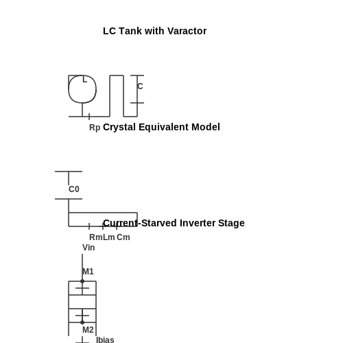
2.3 Tuning Elements: Varactor Diodes and Their Characteristics
Varactor diodes, also known as varicap diodes, are semiconductor devices whose capacitance varies with the applied reverse bias voltage. They are widely used in voltage-controlled oscillators (VCOs) for frequency tuning due to their nonlinear capacitance-voltage (C-V) characteristics. Unlike conventional diodes, varactors are optimized for capacitive behavior rather than rectification.
Physical Operation and C-V Relationship
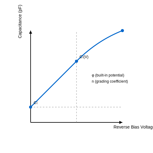
The capacitance of a varactor diode arises from the depletion region formed at the p-n junction under reverse bias. As the reverse voltage increases, the depletion region widens, reducing the junction capacitance. This behavior can be modeled by:
Where:
- Cj is the junction capacitance at applied voltage V
- C0 is the zero-bias capacitance
- φ is the built-in potential (typically 0.7V for silicon)
- n is the grading coefficient (0.5 for abrupt junctions, 0.33 for graded junctions)
Key Performance Parameters
The quality factor (Q) and tuning ratio are critical metrics for varactor diodes in VCO applications:
where Rs is the series resistance. High Q factors (>100 at GHz frequencies) are essential for low-phase-noise oscillators. The tuning ratio describes the capacitance variation range:
Modern hyperabrupt junction varactors achieve tuning ratios exceeding 10:1, enabling wideband VCOs.
Practical Implementation Considerations
When integrating varactors into VCO designs, several factors must be considered:
- Bias network isolation: RF chokes and bypass capacitors prevent oscillator signal leakage into the control voltage source
- Temperature stability: The C-V characteristic shifts with temperature (typically -100 to -300 ppm/°C)
- Nonlinearity: Higher-order terms in the C-V relationship can introduce harmonic distortion
- Flicker noise: Low-frequency noise upconversion affects phase noise performance
Advanced Varactor Technologies
Recent developments include:
- MOS varactors: Using CMOS gate oxide capacitance with superior linearity
- Ferroelectric varactors: Employing tunable dielectric materials for higher Q factors
- MEMS varactors: Microelectromechanical systems with digitally tunable capacitance
The figure below shows a typical C-V curve for commercial varactor diodes:
3. Phase-Locked Loops (PLLs) and Frequency Synthesis
Phase-Locked Loops (PLLs) and Frequency Synthesis
Basic PLL Architecture
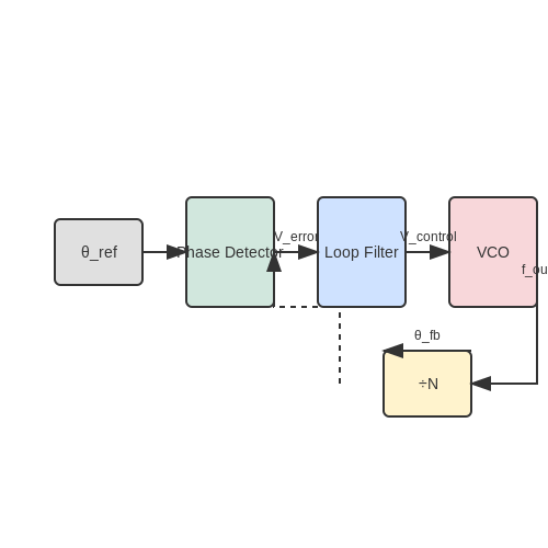
A phase-locked loop (PLL) is a feedback control system that synchronizes the phase and frequency of an output signal with a reference input signal. The core components of a PLL include:
- Phase Detector (PD): Compares the phase difference between the reference signal and the feedback signal, producing an error voltage proportional to the phase difference.
- Loop Filter (LF): A low-pass filter that smoothens the error signal from the phase detector, removing high-frequency noise and ripple.
- Voltage-Controlled Oscillator (VCO): Generates an output signal whose frequency is controlled by the filtered error voltage.
- Frequency Divider (Optional): Divides the VCO output frequency to match the reference frequency, enabling frequency synthesis.
Mathematical Analysis of PLL Dynamics
The behavior of a PLL can be analyzed using linear control theory. The phase transfer function of a second-order PLL is derived as follows:
where:
- \( \theta_{in}(s) \) and \( \theta_{out}(s) \) are the input and output phase signals in the Laplace domain.
- \( K_{PD} \) is the phase detector gain (V/rad).
- \( K_{VCO} \) is the VCO gain (rad/s/V).
- \( F(s) \) is the loop filter transfer function.
For a passive lead-lag filter with transfer function:
the closed-loop transfer function becomes:
where \( K = K_{PD} K_{VCO} \). The natural frequency \( \omega_n \) and damping factor \( \zeta \) are:
Frequency Synthesis Techniques
PLLs are widely used in frequency synthesis, where a stable reference frequency \( f_{ref} \) is multiplied to generate higher frequencies. The output frequency \( f_{out} \) is given by:
where \( N \) is the division ratio of the feedback divider. Fractional-N synthesis allows finer frequency resolution by dynamically switching between integer division ratios, achieving an effective fractional \( N \).
Phase Noise and Jitter in PLLs
Phase noise is a critical performance metric in PLLs, arising from oscillator noise, reference noise, and divider noise. The single-sideband phase noise \( \mathcal{L}(f) \) is modeled as:
where \( S_{\phi}(f) \) is the power spectral density of phase fluctuations. Jitter, the time-domain counterpart of phase noise, is computed by integrating \( S_{\phi}(f) \) over the relevant bandwidth.
Applications of PLLs
- Clock Generation: PLLs provide low-jitter clock signals for microprocessors and digital systems.
- Wireless Communication: Used in RF transceivers for carrier recovery and frequency synthesis.
- Data Recovery: Clock and data recovery (CDR) circuits in high-speed serial links rely on PLLs.
Modern PLL Implementations
Advanced PLL designs incorporate digital phase detectors (e.g., bang-bang PD), adaptive bandwidth control, and all-digital PLLs (ADPLLs) for improved performance in nanometer-scale CMOS processes.
3.2 Modulation and Demodulation in Communication Systems
Fundamentals of Modulation in VCO-Based Systems
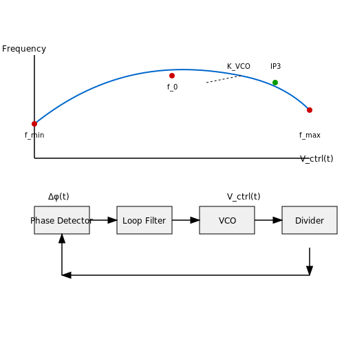
Voltage-controlled oscillators (VCOs) serve as the core component in frequency modulation (FM) and phase modulation (PM) systems due to their inherent voltage-to-frequency conversion property. The output frequency fout of a VCO is given by:
where f0 is the center frequency, KVCO is the tuning sensitivity (Hz/V), and Vin is the input control voltage. For FM, the modulating signal m(t) directly varies Vin, producing an instantaneous frequency deviation:
Phase-Locked Loops for Demodulation
In demodulation applications, VCOs are often embedded within phase-locked loops (PLLs). The PLL tracks the phase of the incoming FM signal, converting frequency variations back into the original baseband signal. The loop filter's output voltage Vctrl becomes a replica of m(t):
where Δφ(t) is the phase error detected by the phase detector. This closed-loop operation suppresses high-frequency noise, making PLL-based demodulators robust in low-SNR environments.
Nonlinear Effects and Distortion
Practical VCOs exhibit nonlinear tuning characteristics, introducing harmonic distortion in wideband FM systems. The third-order intercept point (IP3) of the VCO's f-V curve determines spurious emission levels. For a modulating signal with amplitude A, the distortion power Pdist scales as:
This necessitates predistortion linearization techniques in software-defined radio (SDR) transceivers.
Real-World Implementation: Cellular Systems
In 4G LTE base stations, VCO-based modulation achieves channel bandwidths up to 20 MHz using fractional-N PLLs with sigma-delta dithering. The error vector magnitude (EVM) performance is critically dependent on the VCO's phase noise profile L(f):
where H(f) is the receiver's equivalent noise bandwidth. Modern designs employ LC-tank VCOs with Q-factors exceeding 30 to meet the -40 dB EVM requirement.
Advanced Techniques: Polar Modulation
Envelope tracking transmitters use dual-VCO architectures where one VCO generates the phase component while another modulates the supply voltage. The Cartesian-to-polar conversion is performed digitally:
This approach achieves power amplifier efficiencies above 60% in 5G millimeter-wave systems.
3.3 Signal Generation in Test and Measurement Equipment
Voltage-controlled oscillators (VCOs) are fundamental in test and measurement equipment, providing precise frequency modulation for signal generation. Their ability to produce stable, tunable waveforms makes them indispensable in applications such as spectrum analyzers, network analyzers, and arbitrary waveform generators.
Frequency Synthesis and Phase-Locked Loops
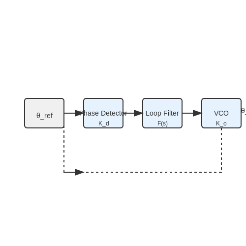
Modern test equipment often employs phase-locked loops (PLLs) in conjunction with VCOs to achieve high-frequency stability. The PLL compares the VCO output phase with a reference signal, adjusting the control voltage to minimize phase error. The closed-loop transfer function of a PLL is given by:
where Kd is the phase detector gain, Ko is the VCO gain, and F(s) represents the loop filter transfer function. For a second-order PLL with a passive lag-lead filter:
This configuration provides improved noise rejection while maintaining stability.
Wideband Signal Generation Techniques
High-performance test equipment requires VCOs with wide tuning ranges. Varactor-tuned LC oscillators offer octave-spanning frequency coverage, where the resonant frequency follows:
Cj represents the voltage-dependent varactor capacitance, while Cpar accounts for parasitic capacitances. The tuning linearity is often improved through:
- Hyperabrupt junction varactors with tailored doping profiles
- Switched capacitor banks for discrete frequency steps
- Digital predistortion algorithms in software-defined instruments
Phase Noise Considerations
In precision measurement systems, VCO phase noise directly impacts instrument resolution. The Leeson model describes the single-sideband phase noise spectral density:
where fm is the offset frequency, Q the resonator quality factor, and fc the flicker noise corner. High-Q resonators (e.g., sapphire-loaded cavities or MEMS structures) can achieve phase noise below -150 dBc/Hz at 1 MHz offset in microwave applications.
Modulation Capabilities
Modern arbitrary waveform generators implement direct digital synthesis (DDS) with VCO-based clock multipliers. The digital phase accumulator generates precise frequency steps:
When combined with a high-speed DAC, this allows complex modulation schemes including:
- Quadrature amplitude modulation (QAM) up to 256-QAM
- Ultra-wideband (UWB) pulse shaping
- Chirp signals for radar simulation
Advanced instruments use segmented memory architectures to store and replay modulated waveforms with nanosecond timing resolution.
Calibration and Compensation
Temperature drift in VCOs necessitates active compensation in metrology-grade equipment. A common approach uses polynomial correction:
where coefficients anm are determined during factory calibration. Real-time temperature monitoring with embedded sensors enables compensation loops with < 0.1 ppm/°C stability.
4. Phase Noise and Its Impact on Signal Integrity
4.1 Phase Noise and Its Impact on Signal Integrity
Fundamentals of Phase Noise
Phase noise is a critical metric in oscillator performance, quantifying the short-term frequency instability of a signal. It manifests as random fluctuations in the phase of an oscillator's output, leading to spectral spreading around the carrier frequency. Mathematically, phase noise L(f) is defined as the ratio of the power spectral density (PSD) of phase fluctuations at an offset frequency f from the carrier to the total signal power:
where Sϕ(f) is the single-sided PSD of phase fluctuations, and Pcarrier is the carrier power. Phase noise is typically expressed in dBc/Hz (decibels relative to the carrier per hertz bandwidth).
Sources of Phase Noise
Phase noise arises from both fundamental and technical sources:
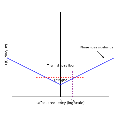
- Thermal noise (Johnson-Nyquist noise): A fundamental limit caused by random electron motion in resistive components, scaling with temperature and bandwidth.
- Flicker noise (1/f noise): Dominates at low offset frequencies due to defects in semiconductor materials or surface states in active devices.
- Nonlinear effects: Amplitude-to-phase conversion in active devices introduces additional noise modulation.
- Power supply noise: Couples into the oscillator's control voltage or bias points, perturbing frequency stability.
Leeson's Model for Phase Noise
Leeson's equation provides a semi-empirical model for phase noise in feedback oscillators:
Here, F is the noise figure of the active device, k is Boltzmann's constant, T is temperature, f0 is the carrier frequency, QL is the loaded quality factor of the resonator, and fc is the flicker noise corner frequency. The model highlights the inverse relationship between QL and phase noise, emphasizing the importance of high-Q resonators.
Impact on Signal Integrity
Phase noise degrades system performance in several ways:
- Communication systems: Causes inter-symbol interference (ISI) in high-data-rate links and raises error vector magnitude (EVM) in modulated signals.
- Radar and sensing: Reduces range resolution and increases false detection rates due to spectral leakage.
- Frequency synthesizers: Introduces spurious sidebands and limits channel selectivity in phase-locked loops (PLLs).
Measurement Techniques
Phase noise is typically characterized using:
- Spectrum analyzers: Direct measurement of the power spectrum, though limited by the instrument's own phase noise floor.
- Phase detector methods: Compare the oscillator under test against a low-noise reference using a mixer and baseband analyzer.
- Delay-line discriminators: Convert phase fluctuations into amplitude variations for high-sensitivity measurements.
Mitigation Strategies
Key approaches to minimize phase noise include:
- High-Q resonators: Use dielectric or crystal resonators to maximize QL and reduce thermal noise contribution.
- Low-noise active devices: Select transistors with low flicker noise corners (e.g., GaAs HEMTs or SiGe HBTs).
- Optimal biasing: Avoid regions of strong AM-to-PM conversion in amplifiers.
- Supply filtering: Employ low-noise regulators and decoupling networks to minimize injected noise.
Practical Trade-offs
Designers must balance phase noise against other metrics like tuning range, power consumption, and form factor. For instance, increasing resonator Q often reduces tuning bandwidth, while lowering flicker noise may require higher bias currents. Advanced techniques like subsampling PLLs or injection-locked oscillators can further optimize performance in specific applications.
4.2 Techniques for Improving Frequency Stability
Temperature Compensation
Frequency drift due to temperature variations is a dominant source of instability in VCOs. The relationship between frequency (f) and temperature (T) can be modeled as:
where f0 is the nominal frequency at reference temperature T0, and α, β are linear and quadratic temperature coefficients. Compensation techniques include:
- Thermistor Networks: Negative temperature coefficient (NTC) thermistors adjust bias currents to counteract frequency drift.
- Varactor Diode Biasing: Temperature-dependent voltage offsets applied to tuning varactors compensate for LC tank variations.
- Silicon-on-Insulator (SOI) Designs: Reduce substrate coupling losses that exacerbate thermal sensitivity.
Phase-Locked Loop (PLL) Stabilization
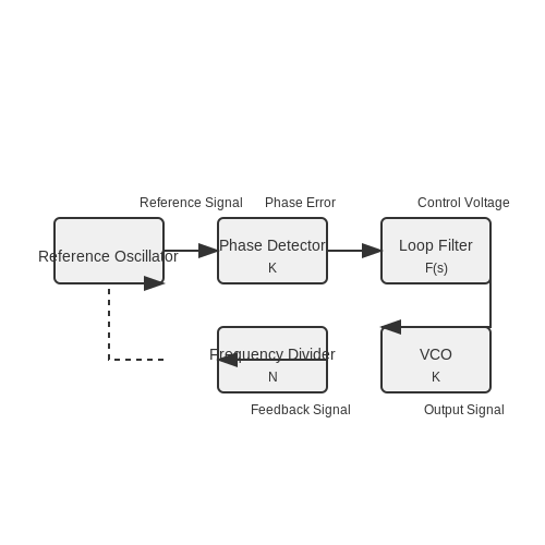
PLLs improve long-term stability by locking the VCO output to a high-stability reference oscillator (e.g., crystal or atomic clock). The loop filter design critically affects stability:
where Kd is the phase detector gain, Kv is the VCO gain, F(s) is the loop filter transfer function, and N is the divider ratio. Key considerations:
- Loop Bandwidth: Narrow bandwidth reduces reference noise but increases settling time.
- Higher-Order Filters: Additional poles suppress reference spurs at the cost of phase margin.
Low-Noise Power Supply Design
Power supply ripple modulates VCO frequency via supply pushing (Kps). The resulting phase noise (L(f)) is given by:
where SV(f) is the power spectral density of supply noise. Mitigation strategies:
- Low-Dropout Regulators (LDOs): Achieve >60dB PSRR at VCO operating frequencies.
- Active Noise Cancellation: Feed-forward correction injects anti-phase noise into the supply rail.
Mechanical Stabilization
Microphonics and vibration induce frequency modulation through:
where Km is the mechanical sensitivity, a is acceleration, and fm is vibration frequency. Countermeasures include:
- Isolation Mounts: Elastomeric or active piezoelectric dampers attenuate vibrations.
- Monolithic Resonators: MEMS-based designs reduce sensitivity to board flexure.
Advanced Materials and Fabrication
Substrate and resonator material choices significantly impact stability:
| Material | TCF (ppm/°C) | Q Factor |
|---|---|---|
| Silicon | 30-50 | 10-100 |
| Quartz | 0.1-1 | 104-105 |
| AlN | 15-25 | 103-104 |
Emerging techniques like 3D integration and superconducting resonators push Q factors above 106 at cryogenic temperatures.
4.3 Trade-offs Between Tuning Range and Phase Noise
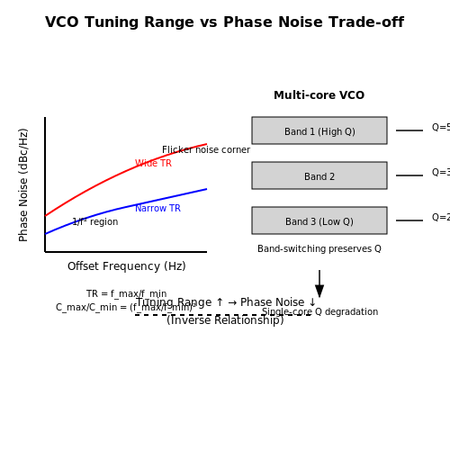
Voltage-controlled oscillators (VCOs) inherently exhibit a fundamental trade-off between tuning range and phase noise performance. This relationship arises from the underlying physics of oscillator design, where broadening the frequency range often compromises spectral purity. The Leeson-Cutler equation provides a theoretical foundation for understanding this phenomenon:
where F represents the noise factor, k is Boltzmann's constant, T is temperature, Psig is the signal power, f0 is the oscillation frequency, QL is the loaded quality factor, fm is the offset frequency, and fc is the flicker noise corner frequency.
Mechanisms of Phase Noise Degradation
As tuning range increases, several effects contribute to phase noise degradation:
- Q-factor reduction: Wider tuning typically requires lower-Q resonator designs, directly impacting the 1/f2 region of the phase noise spectrum.
- Active device nonlinearities: Extended tuning forces active devices to operate across broader bias conditions, increasing AM-to-PM conversion and flicker noise upconversion.
- Power supply sensitivity: Tuning elements (varactors, switched capacitors) often exhibit higher supply voltage sensitivity, translating power supply noise into phase noise.
Quantitative Trade-off Analysis
The tuning range-phase noise trade-off can be modeled by considering varactor properties in LC-tank VCOs. The maximum achievable tuning range TR relates to the tank capacitance ratio:
Meanwhile, phase noise at a given offset Δf depends on tank Q and carrier power P0:
Since Q degrades with increasing Cmax/Cmin ratio, we observe an inverse square relationship between phase noise and tuning range capability.
Practical Design Compromises
Modern VCO implementations employ several strategies to mitigate this trade-off:
- Band-switching architectures: Discrete capacitor banks maintain high Q within sub-bands while achieving wide overall tuning.
- Multi-core oscillators: Parallel VCO cores with overlapping ranges combine optimal phase noise and tuning characteristics.
- Process-specific optimizations: In CMOS designs, accumulation-mode varactors provide better Q than inversion-mode alternatives for a given tuning ratio.
Advanced wireless systems like 5G mmWave transceivers demonstrate these trade-offs clearly. A 28 GHz VCO targeting 30% tuning range might achieve -110 dBc/Hz at 1 MHz offset, while narrowing to 15% range could improve phase noise by 4-6 dB under identical power constraints.
Emerging Techniques
Recent research directions show promise for breaking traditional limitations:
- Bulk acoustic wave (BAW) resonators: Achieve Q factors >1000 while maintaining moderate tuning through piezoelectric effects.
- Optoelectronic oscillators: Leverage optical delay lines for ultra-low phase noise with electronic tuning.
- Machine learning optimization: Automated co-synthesis of tuning and noise parameters across process corners.
5. Key Research Papers and Books on VCO Design
5.1 Key Research Papers and Books on VCO Design
- PDF Microsoft Word - master thesis.doc - Cornell University — The voltage controlled oscillator (VCO) is one of the most important building blocks in modern communication applications such as microprocessor clock generation, wired and wireless communications, system synchronization, and frequency synthesis. The design of high performance VCOs has been increasingly more important and still is an active research area. Research on VCOs for the past decade ...
- Design and Analysis of CMOS LC Voltage Controlled Oscillator in 32nm ... — Abstract This thesis deals with the design and comparative analysis of di erent architectures of on-chip LC voltage controlled oscillators. The design is implemented using IBM 32nm design process and the kit inductors and varactors are used to make the resonator. Di erent VCO architectures have been studied in terms of their phase noise, tuning range, voltage swing and the area. The aim of ...
- CMOS Voltage-Controlled Oscillators - Wiley Online Library — This article addresses the fundamentals of voltage-controlled oscillators (VCOs) in CMOS technologies. The article discusses general stability and oscillation conditions, addresses basic circuit topologies, such as cross-coupled differential pair and three-point oscillators, and then discusses noise mechanisms and circuit techniques to reduce ...
- PDF Voltage-controlled — VOLTAGE-CONTROLLED oscillators (VCOs) play a key role in modern radio frequency (RF) integrated cir-cuit (IC) multistandard transceivers and, therefore, are subject to continuous research efforts that push the boundaries of their multifaceted performance/power efficiency in the state-of-the-art applications and integration technologies [1]-[5].
- PDF RF and Microwave Transistor Oscillator Design — Wideband voltage-controlled oscillators are used in a variety of RF and microwave sys-tems, including broadband measurement equipment, wireless and TV applications and military electronic countermeasure systems.
- (PDF) Design of 5.1 GHz ultra-low power and wide tuning ... - ResearchGate — PDF | p> The objective of the proposed work is to demonstrate the use of a hybrid approach for the design of a voltage-controlled oscillator (VCO) which... | Find, read and cite all the research ...
- Design of a 4.2-to-5.1 GHz Ultralow-Power Complementary Class-B/C ... — Request PDF | Design of a 4.2-to-5.1 GHz Ultralow-Power Complementary Class-B/C Hybrid-Mode VCO in 65-nm CMOS Fully Supported by EDA Tools | Optimal voltage-controlled oscillator (VCO) design for ...
- Low Power VCO Design in CMOS - ResearchGate — Download Citation | Low Power VCO Design in CMOS | The performance of voltage controlled oscillators (VCO) is of extreme importance for any telecommunication or data communication system. This ...
- PDF Analysis and Design of Low-Phase-Noise Integrated Voltage-Controlled ... — A brief introduction to oscillators is presented in Chapter 2, covering basic properties of integrated oscillators together with a survey over existing phase noise models, to serve as a background infor- mation on design related issues and research in this area.
- PDF Low Phase-Noise VCO Design — Draper Laboratory is using a voltage-controlled oscillator (VCO) for mixed-signal processing of a microelectromechanical gyroscope. This thesis studies the design of a new VCO which meets existing circuit specifications with minimal phase noise.
5.2 Online Resources and Datasheets for Common VCO ICs
- Understanding Voltage Controlled Oscillators: VCO Basics and 555 Timer ... — The voltage-controlled oscillators are fundamental in many applications, they are used in applications including signal generators, signal modulations such as Fm and PM, and phase-locked loops such as frequency synthesizers for communication and audio synthesizers for music production. How Does a Voltage Controlled Oscillator Work?
- Voltage Controlled Oscillators (VCOs): Types, Characteristics, and ... — Explore the main types of Voltage Controlled Oscillators (VCOs), including RC, LC, crystal, multivibrator, and ring oscillators. Learn about their characteristics, functions, and applications in electronics.
- PDF Design of a High Performance 5.2 GHz Low Phase Noise Voltage Controlled ... — Abstract—In this paper, a novel Figure of Merit (FOM), low phase noise, LC-tank voltage-controlled oscillator (VCO) is presented. The work presents a fully integrated 5.2 GHz VCO designed in a 90nm CMOS process. The proposed VCO features a worst-case phase noise of -130.10dBc/Hz and -133.00 dBc/Hz at 600 kHz and 1 MHz frequency offset from 5.2GHz carrier is achieved. An optimization ...
- PDF Design of an 800 MHz Voltage Controlled Oscillator — 1.1 VCO Architecture A voltage-controlled oscillator (VCO) is an electronic oscillator whose output fre- quency is proportional to its input voltage. An oscillator produces a periodic AC signal, and in VCOs, the oscillation frequency is determined by voltage.Voltage- controlled oscillators come in various of topologies, including ring oscillators,
- PDF Surface Mount (SMT) Voltage Controlled Oscillator (VCO ... - Pasternack — The PE2V011 is a High Reliability Low Noise Voltage Controlled Oscillator (VCO) which covers a 4.8 GHz to 5.2 GHz frequency band with a voltage tuning range from 0V to 3.0V.
- 5.5: Voltage-Controlled Oscillator (VCO) - Engineering LibreTexts — The design of a broadband VCO is relatively complex, with issues of simultaneous oscillation at multiple frequencies, phase noise, and power efficiency being of primary concern. In a battery-powered communication device the power drawn by the VCO is a substantial fraction of the total power consumed by the RF front end.
- PDF Lab 6. Voltage-Controlled Oscillator — In this lab exercise, we will construct a voltagecontrolled oscillator with surface- -mounted components on a PCB which was laid out for that purpose. We will then measure the VCO, characterize its performance across its tuning range, and compare it to the Xtal oscillator.
- PDF Microsoft Word - Voltage Controlled Oscillator.doc — Voltage Controlled Oscillators voltage controlled oscillator is a rather simple device in theory—it's simply an oscillator whose frequency is related to control voltage. ( t ) C v
- PDF LC Voltage-Controlled Oscillators - Fudan University — Boost the impedance at each common-source node, avoiding Q-degradation Improve the oscillating amplitude voltage, and voltage-limited moves into current-limited
- PDF Low Phase-Noise VCO Design — Draper Laboratory is using a voltage-controlled oscillator (VCO) for mixed-signal processing of a microelectromechanical gyroscope. This thesis studies the design of a new VCO which meets existing circuit specifications with minimal phase noise.
5.3 Advanced Topics: MEMS-Based VCOs and Future Trends
- PDF Chapter 5 Voltage-Controlled Oscillators and Frequency Dividers - Springer — Voltage-Controlled Oscillators and Frequency Dividers Jri Lee 5.1 Considerations ofVCOs Voltage-controlled oscillators (VCOs) and frequency dividers play critical roles in all synchronous circuits. They comprise the core components in phase-locked sys-tems, sometimes necessitating co-design and having great influence on the overall performance.
- MEMS-based LC tank with extended tuning range for ... - PUBLICATIONS — 7.5% and 25%. The LC tank allowed the design of MEMS-based voltage-controlled oscillators (VCOs) with an overall tuning better than 60% in the frequency range 2.15GHz-3.85GHz and two separate regions of continuous tuning range. The VCO prototype will be fabricated on Surface Mount Technology on RO4350 laminate.
- MEMS‐based LC tank with extended tuning range for multiband ... — The LC tank allowed the design of MEMS-based voltage-controlled oscillators (VCOs) with an overall tuning better than 60% in the frequency range 2.15 GHz-3.85 GHz and two separate regions of continuous tuning range. ... higher than 60 at 3 GHz. By using the equivalent π model circuit in Figure 12, the S parameters were fitted in Advanced ...
- CMOS voltage-controlled oscillator with high-performance MEMS tunable ... — LC CMOS voltage-controlled oscillators (VCOs) with tunable inductors are essential for high-performance, multi-band communication systems, such as IoT applications and 5G communication. However, VCOs that use CMOS tunable inductors have difficulty in achieving high RF performance due to the low Q-factor of the inductor. In addition, previously reported CMOS VCOs integrated with MEMS inductors ...
- PDF Design and Analysis of High Performance Voltage Controlled Oscillators — CMOS, the design of robust and high-performance CMOS oscillators, more specifically, voltage-controlled oscillators (VCOs), has become extremely important. 1.1 VCO Metrics The key metrics of a VCO consist of: oscillation frequency, tuning range, phase noise, and power consumption. The frequency of oscillation is determined by the
- PDF Laboratory 2: Voltage Controlled Oscillator - LTH, Lunds Tekniska Högskola — VCOs play a key role in LO/clock generation units in almost all analog and digital embedded systems. Briefly speaking, they generate an oscillatory signal whose frequency is dependent on an input voltage level. There are various types of VCOs such as inverter-based ring oscillators, differential ring oscillators, and LC oscillators.
- Wideband Voltage Controlled Oscillator (VCO) For RF Applications — This Major Qualifying Project involves the design of a voltage controlled oscillator (VCO) for radio-frequency (RF) applications. Voltage controlled oscillators are electronic circuits designed to produce a periodic sinusoidal signal whose frequency is dependent on the voltage applied at the input [1]. Instances where VCOs find use are in ...
- PDF Basic LC VCOs - UCLA Henry Samueli School of Engineering and Applied ... — Basic LC VCOs Behzad Razavi ... • Cross-Coupled Oscillator • VCO Techniques • Discrete Tuning. 3 Voltage-Controlled Oscillators zCenter Frequency zTuning Range: - Band of Interest - PVT Variations zGain (Sensitivity) zSupply Rejection zTuning Linearity zIntrinsic Jitter zOutput Amplitude. 4 Feedback Oscillator. 5 One-Port View
- PDF LC-tank CMOS Voltage-Controlled Oscillators using High Quality ... — LC-tank CMOS Voltage-Controlled Oscillators using High Quality Inductors Embedded in Advanced Packaging Technologies A Dissertation Presented to The Academic Faculty by Sangwoong Yoon In Partial Fulfillment of the Requirements for the Degree Doctor of Philosophy in the School of Electrical and Computer Engineering
- PDF Lab 6. Voltage-Controlled Oscillator - University of Illinois Urbana ... — Lab 6. Voltage-Controlled Oscillator . In this lab exercise, we will construct a voltagecontrolled oscillator with surface- -mounted components on a PCB which was laid out for that purpose. We will then measure the VCO, characterize its performance across its tuning range, and compare it to the Xtal oscillator. Active Buffer Design