Applied Flip-Flops and Latches
1. Definition and Functionality
1.1 Definition and Functionality
In the realm of digital electronics, the concepts of flip-flops and latches are pivotal for understanding the internal workings of memory devices, sequential circuits, and various forms of data storage. Both components serve to maintain a certain state, but they differ significantly in their operational characteristics and applications. Thus, a comprehensive grasp of their definitions and functionalities sets the foundation for exploring more complex systems.
Fundamental Definitions
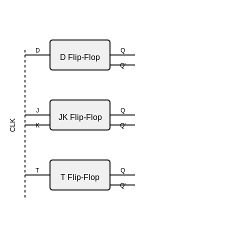
A latch is a fundamental bistable circuit that is capable of storing one bit of information. It is level-sensitive, meaning it can change its output state based on the input levels present at its control (or enable) terminals. Common types of latches include the SR (Set-Reset) latch, D (Data) latch, and JK latch. In contrast, a flip-flop is a more advanced storage element that is edge-sensitive, toggling its output only on the rising or falling edge of a clock signal. The most commonly used flip-flops are the D flip-flop, JK flip-flop, and T (Toggle) flip-flop.
Operational Mechanisms
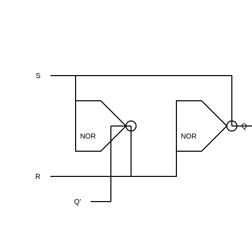
To understand the key functionality of latches and flip-flops, one must first delve into the mechanisms that govern their operations. A typical SR latch, constructed from two cross-coupled NOR gates, retains its state until an external signal activates either the 'Set' or 'Reset' input. The logic table elucidates this operation:
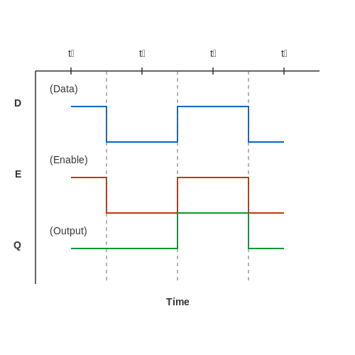
On the other hand, a D latch captures the value of the data input (D) whenever the enable signal is active (typically when it is high). The transition occurs when this enable signal goes low, at which point the latch retains the last captured data:
Transition to Flip-Flops
Unlike latches, flip-flops incorporate clock signals to synchronize operations across multiple components. The D flip-flop, for instance, transfers the data present at its D input to its output (Q) on a specific clock edge, ensuring stable data capture. This edge-triggered nature minimizes the risk of race conditions that might occur in level-sensitive latches. Such behavior is especially crucial in synchronous systems where timing dictates operational integrity.
The transfer function of the D flip-flop can be expressed mathematically as follows:
Applications of Latches and Flip-Flops
The applications of both latches and flip-flops are wide-ranging and significant in today's digital circuits:
- Memory storage: Latches are often used in simple memory devices, while flip-flops form the backbone of register files and cache memories in processors.
- Data synchronization: Flip-flops are essential in synchronizing data transfer between asynchronous domains within integrated circuits.
- Frequency division: T flip-flops are employed in frequency dividers for clock generation tasks.
- Finite state machines: Both latches and flip-flops are utilized in designing state machines for various digital control applications.
In conclusion, understanding the definitions and functionalities of latches and flip-flops not only clarifies their operational differences but also illuminates their roles in sophisticated electronic systems. This knowledge lays the groundwork for more detailed explorations into how these elements interact within various circuit designs and applications.
1.2 Types of Flip-Flops
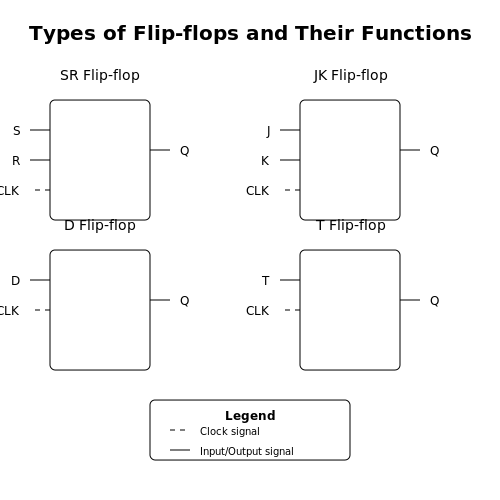
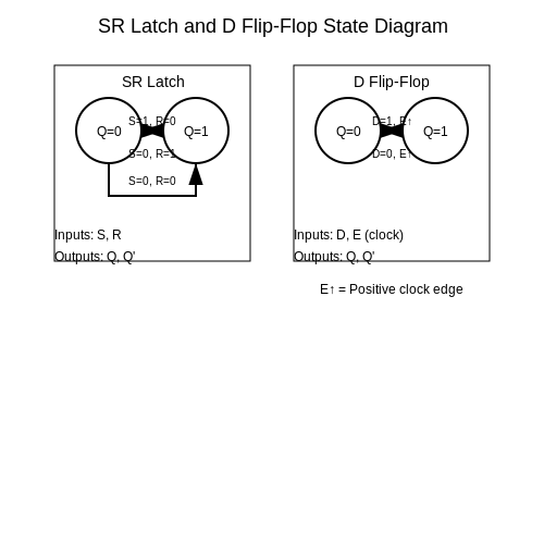
In digital electronics, flip-flops are fundamental building blocks used in a variety of applications, from simple data storage to complex state machines. Understanding the various types of flip-flops is crucial for engineers and researchers as they design and implement systems that rely on these devices for memory and control functions. Flip-flops can be classified based on their characteristics and operational modes. The primary types include the SR (Set-Reset), D (Data), JK, and T (Toggle) flip-flops. Each type serves a specific purpose and offers distinct advantages in different applications.SR Flip-Flops
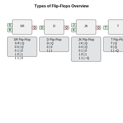
The SR flip-flop operates with two inputs, typically labeled S (Set) and R (Reset). The state of the flip-flop can be set to high or low based on these inputs. When S is high, the Q output becomes high, while setting R high forces Q to low. A key feature of the SR flip-flop is that the condition where both S and R are high is considered invalid, as it results in an indeterminate state. To visualize its operation, consider a truth table where the inputs S and R determine the output Q:- S = 0, R = 0: Q remains unchanged.
- S = 1, R = 0: Q becomes 1 (Set).
- S = 0, R = 1: Q becomes 0 (Reset).
- S = 1, R = 1: Q enters an indeterminate state.
D Flip-Flops
The D flip-flop simplifies the use of the SR flip-flop by eliminating the indeterminate state. The D flip-flop has a single data input (D) and a clock input (CLK). On the leading edge of the clock pulse, the flip-flop captures the value of D and transfers it to the output Q. This functionality allows for clean data transfer and storage:- When D = 0: Q remains unchanged on the clock pulse.
- When D = 1: Q is set to 1 on the clock pulse.
JK Flip-Flops
The JK flip-flop is a refinement of the SR flip-flop that resolves the issue of invalid states. It features inputs J and K that can toggle the state of the output based on the clock signal. The characteristic behavior of the JK flip-flop is defined as follows:- J = 0, K = 0: No change.
- J = 1, K = 0: Set Q to 1.
- J = 0, K = 1: Reset Q to 0.
- J = 1, K = 1: Toggle the output state.
T Flip-Flops
Finally, the T flip-flop, or toggle flip-flop, is a specialized case of the JK flip-flop. It features a single toggling input (T) and operates by changing its state with every clock pulse when T is high. Thus, it can be summarized as:- T = 0: No change.
- T = 1: Toggle the previous state of Q.
1.3 Key Terms and Concepts
In the realm of digital electronics, precisely defined key terms and concepts are essential for understanding the intricate workings of flip-flops and latches. These memory elements form the backbone of sequential circuits, playing crucial roles in data storage and control logic. This section delineates foundational definitions and principles that underpin their functionality.
Flip-Flops
A flip-flop is a bistable circuit, meaning it has two stable states and can store one bit of data. The primary types of flip-flops include:
- SR Flip-Flop: Composed of two inputs, Set (S) and Reset (R), this configuration changes state based on the inputs, allowing it to store a binary value.
- D Flip-Flop: Utilizes a single data input (D) and a clock signal. The flip-flop captures the value of D at a specific moment when the clock signal transitions, ensuring synchronized data storage.
- JK Flip-Flop: An enhancement of the SR flip-flop, this version resolves the invalid state condition. It has inputs J and K, allowing toggle functionality—for every clock pulse, the output toggles if both inputs are high.
- T Flip-Flop: A specialized JK flip-flop where the T input determines whether to toggle. This is particularly useful in counters and state machines.
Latches
Unlike flip-flops, latches are level-triggered devices, meaning their output can change as long as the inputs are active. Key latch types include:
- SR Latch: Formed with two cross-coupled NOR or NAND gates, it can be used to create simple memory storage. The inputs set and reset the latch depending on their states.
- D Latch: Similar to the D flip-flop, but operates without a clock. The latch is transparent when the enable signal is active, allowing it to follow the input signal directly until the enable signal is removed.
Timing Analysis
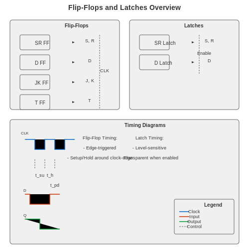
When dealing with flip-flops and latches, timing characteristics such as Setup Time, Hold Time, and Propagation Delay are critical. Each of these parameters affects how reliably data can be stored and transferred within a circuit. The definitions usually are as follows:
- Setup Time (tsu): The minimum time before a clock edge that data must be stable for reliable storage.
- Hold Time (th): The minimum time after the clock edge that data must remain stable to ensure it is correctly captured.
- Propagation Delay (tpd): The time taken for a change at the input of a flip-flop to cause a change at its output.
In practical applications, understanding these timings is essential for designing reliable digital systems, as not adhering to these constraints can lead to metastability and incorrect data storage.
Practical Applications
Flip-flops and latches are omnipresent in today’s electronic circuits, underpinning various applications:
- Data Storage: Basic memory elements like static RAM utilize flip-flops to store data bits.
- Counters: Toggle capabilities of T flip-flops help build up counting circuits used in digital clocks and frequency dividers.
- State Machines: Sequential logic circuits leverage both flip-flops and latches to control the state transitions based on input sequences.
As you explore more advanced configurations and applications, understanding these fundamental terms and concepts provides a solid foundation for analyzing and designing robust digital systems.
2. SR Latch
2.1 SR Latch
The SR latch, or Set-Reset latch, serves as one of the fundamental building blocks in digital electronics. Utilizing two inputs—Set (S) and Reset (R)—the SR latch is a bistable device, meaning it can hold one of two stable states indefinitely until changed by an external event. The practical applications range from memory storage elements to complex state machines, making it essential for engineers and designers in various fields.
Fundamentals of the SR Latch
At its core, the SR latch can be implemented using various means, including discrete components like resistors, capacitors, and transistors, or through logic gate configurations. The simplest form can be designed with two cross-coupled NOR gates or NAND gates. However, to understand its function, we first examine the behavior of the SR latch constructed from NOR gates.
Schematic Representation
The schematic of an SR latch using NOR gates consists of two NOR gates, with the output of each connected to the input of the other. The configuration essentially allows the state of the latch to be maintained as long as power is supplied. The following diagram illustrates this configuration:
Truth Table for SR Latch
The SR latch can be characterized by a truth table that describes the output states based on the inputs:
| Set (S) | Reset (R) | Output Q | Output Q' |
|---|---|---|---|
| 0 | 0 | Q(t) | Q'(t) |
| 1 | 0 | 1 | 0 |
| 0 | 1 | 0 | 1 |
| 1 | 1 | undefined | undefined |
From the truth table, it is evident that:
- When S = 1 and R = 0, the latch sets its output Q to 1, while Q' (the inverse) becomes 0.
- When S = 0 and R = 1, the latch resets Q to 0, and Q' becomes 1.
- When both inputs are 0, the latch retains its previous state, which is vital for its memory function.
- The condition where both S and R are 1 is considered invalid, as it leads to an indeterminate state.
Practical Relevance
The SR latch forms the basis of more complex memory elements, such as flip-flops, which are used in various applications from computer memory to state storage in sequential circuits. Understanding the operation and implications of the SR latch is critical for the design of reliable digital systems.
In advanced applications, variations of the SR latch, including edge-triggered and level-sensitive latches, provide solutions to synchronous design constraints, ensuring that inputs only affect the latch during specific clock cycles. Moreover, these devices are essential for developing memory banks and registers in digital integrated circuits.
2.2 D Latch
Understanding the D Latch
The D latch, also known as a data latch, is a fundamental building block in digital electronics, often utilized in storage elements and state-retaining applications. Unlike its more complex counterparts, such as flip-flops, a D latch responds directly to a control signal while providing a simple yet efficient means of retaining a binary state. The latch's operation hinges on two inputs: data (D) and a control signal, commonly referred to as enable (E) or clock (CLK).
Operational Principles
The basic operational characteristic of the D latch involves its ability to sample the input data (D) during the activated state of the control signal (E). When the control signal is asserted (logic high), the latch 'transfers' the D input to its output (Q). Conversely, when the enable signal is deactivated (logic low), the output Q retains its previous state, regardless of any changes at the input D. This locking behavior is what classifies it as a real-time memory element.
Truth Table
The D latch's behavior can be succinctly summarized through its truth table, defining the relationship among inputs and outputs:
| E (Enable) | D (Data) | Q (Output) |
|---|---|---|
| 0 | X | Q(t-1) |
| 1 | 0 | 0 |
| 1 | 1 | 1 |
In the truth table above, the output Q reflects the state of the data input D when the enable signal E is active. When E is low, the output remains in its last known state, denoted by Q(t-1).
Mathematical Representation
The D latch can also be described mathematically. We can represent its state using the following simple equations:
Where:
- Q(t) is the current state of the output.
- D is the data input.
- E is the enable input; logic high activates the latch.
- Q(t-1) represents the previous state of the output before state change.
Real-World Applications
The D latch finds widespread application in various digital systems due to its fundamental role in data storage and signal processing. Common applications include:
- Memory Storage: Used in static RAM (SRAM) cells for temporary data retention.
- Data Buffering: Employed in data path buffering to synchronize asynchronous data.
- Timing Circuits: Often utilized in timing operations where precise control of data flow is required.
Conclusion
The D latch stands as a cornerstone in digital circuits. Its straightforward functionality, which allows it to hold a state based on a simple conditional input, makes it suitable for numerous practical implementations. A solid understanding of the D latch is essential for engineers and designers involved in both integrated circuit design and digital logic systems.
2.3 Edge-Triggered vs Level-Triggered
Within the field of digital electronics, the behavior and functionality of flip-flops and latches hinge critically on the timing of signal changes. This leads us to distinguish between two fundamental triggering mechanisms: edge-triggered and level-triggered. Understanding these mechanisms not only enriches our theoretical insights but also enhances the practical application of sequential logic circuits in real-world scenarios.Edge-Triggered Devices
Edge-triggered devices, commonly found in the design of synchronous circuits, respond specifically to the transitions (edges) of a control signal, typically a clock. This design enables precise control over when data is captured and allows for the robust operation of a circuit by synchronizing various parts with a common clock signal. The most common edge-triggered device is the D flip-flop. To illustrate, a D flip-flop captures the value at its input (D) only at the moment of the clock's rising or falling edge. This characteristic helps prevent unintended state changes due to noisy signals that may be present during the level of the clock signal. The resulting behavior can be mathematically described by the following equations:- Enhanced reliability: Insensitivity to transient signal variations during the clock signal state.
- Simplified state management: Encourages cleaner state transitions within a synchronous design framework.
Level-Triggered Devices
In contrast, level-triggered devices respond continuously to the input level as long as the control signal remains active. A prime example of this category is the SR latch. Here, the output state depends on the current levels of the inputs rather than specific transitions. For level-triggered devices, the behavior can be represented through:- Immediate feedback: Outputs change instantly in response to changing inputs, leading to simpler designs in certain applications.
- Power considerations: More susceptible to static power consumption as the circuit remains active while the control signal is high.
Practical Implications and Application
Choosing between edge-triggered and level-triggered configurations depends significantly on the application's specific requirements. Edge-triggered systems excel in synchronous environments where precise timing is critical, while level-triggered systems can be advantageous in straightforward setups where speed is of the essence. In systems requiring intricate data handling, such as processors and communication circuits, edge triggering ensures data integrity across varying operational conditions. Conversely, in simpler applications like timers or switches, a level-triggered latch might offer sufficient performance without the complexities of synchronization. Given these principles, engineers and designers can make informed choices that enhance the reliability and functionality of their digital circuits. Understanding the differences between edge-triggered and level-triggered devices not only deepens our comprehension of digital electronics but also lays the foundation for the development of advanced sequential logic applications in modern technology.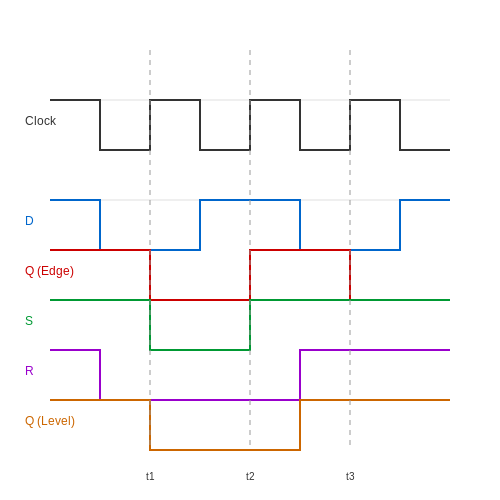
3. Data Storage and Memory Units
3.1 Data Storage and Memory Units
The fundamental purpose of flip-flops and latches extends far beyond simple data storage; they serve as the building blocks for memory units in digital systems. Both components harness the properties of feedback and bistability, allowing them to maintain a stable state until explicitly changed. This section delves into the significance of flip-flops and latches in data storage, exploring their applications and importance in modern electronic systems.
Understanding Data Storage Basics
Data storage methods in electronics can generally be categorized into volatile and non-volatile memories. Volatile memories, such as RAM (Random Access Memory), require continuous power to retain data, whereas non-volatile memories, such as Flash or EEPROM, can retain data even when power is removed. Flip-flops, as a type of bistable multivibrator, are essential in forming registers within RAM, providing a means to store individual bits of data efficiently.
Flip-Flops: The Core of Data Storage
Flip-flops can be fundamentally defined by their ability to store one bit of data. The most common types include:
- D Flip-Flop: Captures the value of the input data line (D) at the clock edge and holds that value until the next clock signal.
- JK Flip-Flop: A versatile version that can toggle its output on specific conditions of the JK inputs, making it more versatile in certain control circuits.
- T Flip-Flop: A specialized flip-flop that toggles its output state whenever the T input is high.
The choice of flip-flop depends on the specific application requirements, such as timing constraints and data flow within the circuit. For example, D flip-flops are widely used in shift registers, data latches, and serial-to-parallel converters due to their inherent simplicity in data storage.
Mathematical Representation of Flip-Flops
To provide a deeper understanding of the operation of flip-flops, we can represent their behavior mathematically. Consider the basic functionality of a D flip-flop:
The output Q next depends on the input D only at the moment the clock (CLK) signal transitions from low to high (0 to 1). The feedback mechanism ensures Q holds its state until the next clock event, emphasizing the stability characteristic of flip-flops.
Latches: Simpler but Effective
Unlike flip-flops, latches are level-triggered devices, which means they can change their output state as long as the enable signal (or control signal) remains high. Common types of latches include:
- S-R Latch: The simplest form of a latch that uses two inputs (Set and Reset) to control the output state.
- D Latch: Functions similarly to the D flip-flop but operates at a level rather than an edge, capturing the input data as long as the enable signal is active.
The choice between a flip-flop and a latch can significantly impact performance in various applications, such as synchronous and asynchronous systems. For instance, latches can introduce additional scenarios of race conditions in sequential circuits if not carefully managed, whereas flip-flops are more robust amid data flow concerns.
Applications of Flip-Flops and Latches in Memory Units
Memory units in modern computing architectures heavily utilize flip-flops and latches. They are integral to data registers, SRAM cells, and even more complex structures like caches. As technology evolves, these memory elements are increasingly being integrated into FPGAs and ASICs, which allow for customized digital logic solutions in various applications, such as:
- Microprocessors: Utilizing flip-flops in instruction and data registers enhances performance by optimizing data access times.
- Digital Signal Processing: Latches and flip-flops allow for efficient management of data pipelining protocols, critical in high-speed synthesis.
- Memory Chips: Flip-flops are fundamental in dynamic RAM (DRAM) and static RAM (SRAM), contributing to their unique operational characteristics.
In summary, both flip-flops and latches represent key fundamental components for data storage within electronic systems. Their ability to store states underpins the operation of more complex memory architectures, emphasizing their continued relevance in modern circuits. As the demand for faster and more efficient memory solutions grows, the understanding and application of these devices will remain paramount in the field of electronics.
3.2 Frequency Dividers
Frequency dividers, also known as frequency dividers or divide-by-N circuits, are crucial components in digital electronics, particularly in applications requiring precise frequency manipulation. These circuits often utilize flip-flops or latches to achieve their operation, allowing for various practical applications ranging from timing generation to signal processing.
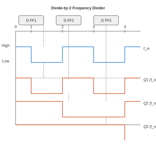
The primary function of a frequency divider is to reduce the frequency of an input signal by a predetermined factor, typically an integer. For instance, a divide-by-2 frequency divider takes a clock signal and produces an output signal that toggles state for every two pulses of the input signal, effectively halving the frequency.
Basic Operation of Frequency Dividers
To understand frequency dividers, let's consider the simplest example: the divide-by-2 frequency divider implemented using a D flip-flop. The working principle is straightforward:
- The D flip-flop captures the input clock signal on the rising (or falling) edge.
- The output (Q) changes state according to the input clock frequency.
- This results in a signal output frequency that is half of the input clock frequency.
The timing diagram for a divide-by-2 circuit using a D flip-flop would show the input clock oscillating at a certain frequency, while the output would transition between two states at half this frequency, illustrating the essence of frequency division.
Mathematical Derivation
To derive the output frequency mathematically, let’s denote:
- fin: the frequency of the input signal
- fout: the frequency of the output signal
- N: the division factor (in the case of a divide-by-2, N = 2)
The relationship between the input and output frequencies can be expressed as:
For a divide-by-2 circuit:
This formula is fundamental to understanding how frequency dividers operate. For example, in a system where the input frequency is 100 MHz, the output frequency of a divide-by-2 circuit would be 50 MHz.
Multistage Frequency Dividers
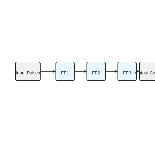
In practical applications, single-stage frequency dividers may not suffice. To achieve larger division factors, designers often employ cascaded flip-flops, forming a multistage frequency divider. Each flip-flop in the series contributes a factor of 2 to the frequency division.
For a divide-by-N system, where N is a power of 2, the configuration would look like this:
Here, n indicates the number of stages or flip-flops used. For example, if we desire a divide-by-8 operation:
Therefore, three D flip-flops would be connected in series, where each flip-flop halves the frequency of the input clock signal at its output.
Applications of Frequency Dividers
Frequency dividers play a pivotal role in various applications:
- Clock Generation: They are often used in microcontrollers and digital systems to generate clock signals of lower frequencies derived from high-frequency oscillators.
- Signal Conditioning: In communication systems, frequency dividers help in manipulating signal frequencies for appropriate transmission and reception.
- Division of Time Bases: Used in timers and counters where specific timing intervals are required.
Understanding the principles of frequency dividers provides foundational knowledge essential for engineers and scientists engaging in design work requiring precise timing and frequency management. These components encapsulate both theoretical aspects and practical implementations in modern electronics.
3.3 State Machines
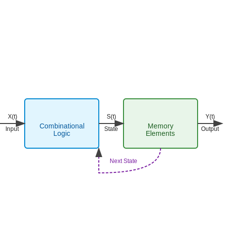
State machines represent a powerful model for designing complex systems in both digital electronics and computer science. A state machine is defined as a computational model comprised of a set of distinct states, transitions between those states, and actions that occur due to input signals or events. This conceptual framework is particularly useful in applications involving flip-flops and latches, where the management of state is critical.
Understanding state machines hinges on the concept of states. Each state is a unique configuration of inputs and outputs, controlled by digital signals. The transition from one state to another is initiated through inputs, which may either trigger a state change or maintain the current state. This process is inherently temporal, meaning it captures the dynamic behavior of systems over time.
Types of State Machines
There are primarily two types of state machines: Mealy and Moore machines. The distinction lies in how outputs are generated:
- Mealy Machine: Outputs depend on both the current state and the input. This can result in quicker response times to changes in input because outputs can change during the state transition.
- Moore Machine: Outputs depend solely on the current state. Although this can simplify design, it may introduce delays since outputs are based only on state configurations.
Mathematical Representation
To mathematically formalize a state machine, consider the following points:
- States (S): A finite set of states.
- Input Alphabet (I): A finite set of inputs.
- Output Alphabet (O): A finite set of outputs (more relevant for Mealy machines).
- Transition Function (T): This function defines how state transitions take place. It can be expressed as \( T: S \times I \rightarrow S \) for Mealy machines or \( T: S \times I \rightarrow S \) with distinct output mapping for Moore machines.
- Output Function (Z): For a Mealy machine \( Z: S \times I \rightarrow O \); for a Moore machine \( Z: S \rightarrow O \).
This structure allows state machines to be designed methodically, offering a predictive mechanism for system behavior under various input conditions.
Real-World Applications
State machines are ubiquitous in many engineering applications:
- Digital Circuit Design: State machines are used to manage complex sequences in processors and control systems.
- Protocol Design: Communication protocols often rely on state machines to manage connections and data flow.
- Embedded Systems: State machines govern the behavior of appliances, toys, and automotive systems, ensuring responsive and reliable outputs.
Furthermore, in programming paradigms, state machines can be utilized to model game development scenarios where game states shift based on player actions, enhancing interactive design.
Conclusion
The use of state machines provides a structured and rigorous approach to managing state-dependent systems. By comprehensively understanding both Mealy and Moore machines, engineers can harness these concepts to improve system design, enhance reliability, and optimize performance across a wide range of applications.
4. Setup and Hold Times
4.1 Setup and Hold Times
Understanding setup and hold times is crucial for reliable digital circuit operation, particularly when designing circuits that utilize flip-flops and latches. These timing parameters are essential in ensuring that data are captured correctly in sequential circuits, avoiding errors that can arise from inadequate timing margins.
Setup Time
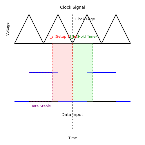
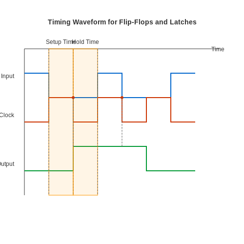
Setup time is defined as the minimum time before the clock edge that the input data must remain stable for the flip-flop or latch to reliably capture that data. Mathematically, it can be denoted as:
Where:
- Ts is the setup time.
- Tclk is the clock edge time.
- Tdata is the time the data input must be stable before the clock edge.
The setup time ensures that the flip-flop has enough time to establish the proper state based on the input data before it samples the data on the clock transition. For instance, if a flip-flop has a specified setup time of 5 ns, the data signal must be stable at least 5 ns prior to the clock transition.
Hold Time
Complementary to setup time, hold time refers to the minimum period after the clock edge during which the data input must remain stable. This is critical because it ensures that the flip-flop maintains its output states correctly without inadvertently changing due to data instability. The hold time can be expressed as:
Where:
- Th is the hold time.
- Tdata is the time the output data must be stable after the clock edge.
- Tclk is the clock edge time.
A typical value for hold times can range from 1 to 3 ns depending on the specific flip-flop technology being used. If the input changes too soon after the clock edge, the output may not settle to the correct value, potentially leading to glitching or incorrect behavior in the overall circuit. Therefore, it is critical that both setup and hold time conditions are met in design configurations.
Practical Relevance and Applications
In real-world applications, understanding and accounting for setup and hold times is vital in high-speed digital circuits such as microprocessors, FPGA designs, and high-speed data communication systems. Violations in these timing constraints can lead to timing hazards, race conditions, and data corruption. Design engineers often use timing analysis tools to simulate and ensure that their designs meet the setup and hold time specifications, particularly in complex systems where signal propagation delays and jitter can complicate potential violations.
In summary, setup and hold times represent critical parameters that ensure reliable operation of digital systems governed by flip-flops and latches. Awareness and incorporation of these times during design will yield robust and fault-tolerant digital circuits.
4.2 Timing Diagrams
Timing diagrams are an essential tool in the visualization and analysis of digital circuits, particularly when working with flip-flops and latches. They depict the state of signals over time, providing clarity on how different components interact within a circuit based on their timing relationships. In this subsection, we will delve into the fundamental aspects of timing diagrams, explore how they are constructed, and discuss their practical relevance in the design and analysis of digital systems.
Understanding Timing Diagrams
A timing diagram represents the states of multiple signals, typically in the form of voltage levels, plotted over time. The transitions between these states indicate when a circuit responds to input signals, making it easier to analyze sequential logic behavior. In essence, timing diagrams allow engineers to observe and verify that various thresholds and conditions are met in a circuit before implementation.
In the context of flip-flops and latches, timing diagrams are particularly important for understanding the relationship between inputs (such as data and clock signals) and outputs (the stored state). For instance, a set-reset latch can be depicted to show how it maintains its state based on input conditions and transitions.
Construction of Timing Diagrams
To create a timing diagram, follow these steps:
- Identify relevant signals: Determine the key signals based on the circuit in question. Typically, this will include the clock signal, data input(s), and output(s).
- Establish time intervals: Decide on a suitable time scale for your diagram. This will ensure that the dynamics can be effectively captured.
- Mark transitions: Using the known characteristics of the flip-flops or latches involved, plot the various states of each signal over time. Focus on when the outputs change states in relation to clock edges and input transitions.
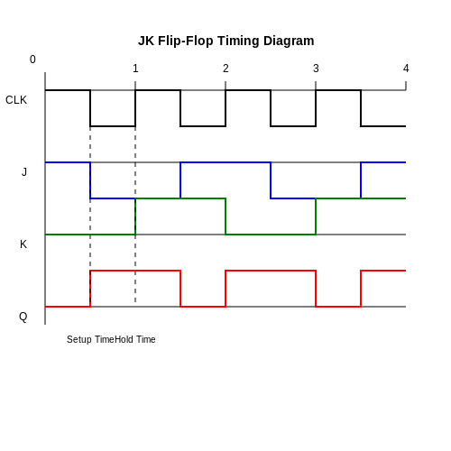
For instance, consider a JK flip-flop. The timing diagram for this component would show changes at the output based on different combinations of J and K inputs across clock cycles.
Example: JK Flip-Flop Timing Diagram
In a simplified timing diagram of a JK flip-flop:
- The clock signal will be displayed as a square wave, rising at regular intervals.
- The J and K inputs will be shown as alternating states (HIGH and LOW) corresponding to the clock cycles.
- The output will toggle according to the specific state rules based on the JK inputs at every clock rising edge.
A graphical representation of such a diagram would showcase how the output follows the defined behavior of the flip-flop, particularly emphasizing the setup and hold times during each transition.
This formula helps to ensure that the flip-flop receives stable inputs during critical intervals around the clock edge, highlighting how timing diagrams relate directly to the theoretical aspects of digital design. Here, T_cycle represents the total period for each clock cycle, while T_setup and T_hold are the minimum times required before and after the clock edge for stability.
Practical Applications of Timing Diagrams
Timing diagrams are critical in various applications:
- Design Verification: Engineers use timing diagrams to confirm that the timing constraints of digital systems are satisfied and that the design will function as expected.
- Debugging: Analyzing timing diagrams helps identify timing-related issues such as race conditions, glitches, or setup/hold violations that could lead to functional failures.
- Communication Protocols: In more complex systems, timing diagrams illustrate the timing relationships essential for communication protocols, ensuring accurate data transfers and synchronization between devices.
In conclusion, mastering timing diagrams is vital for anyone involved in the design and analysis of digital systems. By understanding how to construct and interpret these diagrams, engineers can ensure that their designs meet performance criteria and function reliably in real-world applications.
4.3 Metastability Issues
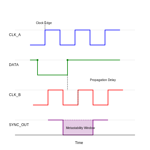
In digital circuits, metastability poses significant challenges, particularly in the context of flip-flops and latches. Understanding metastability requires a grasp of how these devices interact with signals and respond to transitions, especially in systems designed to synchronize multiple clock domains.
Understanding Metastability
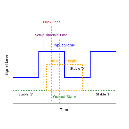
Metastability occurs when a flip-flop or latch is unable to resolve its output to a stable state within the specified time frame after receiving an input signal. This phenomenon often arises during the input signal transition, leading to indeterminate output states. Essentially, the device enters a state where it is caught between logic levels, neither fully high nor fully low. This state can persist for an unpredictable duration, which can lead to improper operation in sequential designs.
Root Causes
Key factors influencing metastability include:
- Setup and Hold Times: Transitions of input signals must respect setup and hold times to prevent metastable states. Violating these timing constraints can induce metastability.
- Clock Domain Crossing: Interfacing signals across different clock domains heightens the risk of metastability due to timing mismatches.
- Noise: External electrical noise can also contribute to inputs being sampled near the transition threshold, increasing the likelihood of entering a metastable state.
The Metastability Model
A commonly used model to describe metastability involves the introduction of a second-order response function. The behavior can be represented by a linear differential equation, where the metastable state can be characterized by a time constant:
Here, \( \tau \) represents the time constant, \( V_{DD} \) is the supply voltage, and \( I_{bias} \) is the biasing current through the transistor. The ability of the device to escape metastability can typically be characterized by a probability function, which indicates the likelihood of the output resolving to a stable state over time.
Implications in Design
In practical applications, metastability can result in severe data integrity issues, particularly in high-speed communication interfaces and clocked systems. Engineers often employ several strategies to mitigate these risks:
- Synchronizers: Utilizing two or more flip-flops in series, known as a synchronizer, can effectively reduce the probability of metastability by allowing additional time for the signal to stabilize.
- Choosing Appropriate Clock Frequencies: Maintaining appropriate clock frequency ratios can alleviate metastability issues at the cost of performance.
- Meta-Stability Analysis: Engineers can make use of simulations to model and analyze metastable behavior and its impacts on digital designs.
Case Studies and Practical Relevance
In communication systems like USB and PCIe, metastability poses challenges due to their reliance on high-speed data transfer. Practical approaches, such as utilizing redundant paths or designs that incorporate error detection and correction mechanisms, help ensure consistent performance despite the risks introduced by metastability.
As digital systems evolve towards higher speeds and lower power consumption, understanding and addressing metastability will remain critical for engineers and designers alike. By anticipating and mitigating the effects of metastability, we can build more robust and reliable systems capable of meeting modern performance requirements.
5. Choosing the Right Flip-Flop or Latch
5.1 Choosing the Right Flip-Flop or Latch
When it comes to digital circuits, selecting the appropriate flip-flop or latch is paramount to achieving desired functionalities and performance characteristics. These memory elements serve as the backbone of sequential circuits, impacting not just reliability and efficiency but also power consumption and speed. Thus, understanding the nuances between various types is essential for optimizing designs.Understanding the Differentiation Between Flip-Flops and Latches
Latches and flip-flops are both bistable devices, meaning they can hold one of two binary states. However, their operational characteristics herald critical differences. A latch is an asynchronous device; it captures data immediately when the enable signal is active. Conversely, a flip-flop is edge-triggered, meaning it changes states only at specific moments defined by clock edges (e.g., rising or falling). This fundamental distinction dictates when and how data is sampled. Understanding this leads to a vital consideration: timing constraints. In applications requiring immediate data representation without the constraints of clock cycles, latches would be prudent. However, for synchronous designs, where timing alignment is paramount, flip-flops are preferred.Application Domains
Different application scenarios favor different types of memory elements:- Data Storage: Flip-flops are commonly found in registers and temporary storage within CPUs and FPGAs. Their synchronous nature fits well in environments requiring deterministic behavior.
- State Machines: In designing finite state machines (FSMs), flip-flops assume a critical role due to their ability to synchronize state transitions effectively.
- Signal Synchronization: Latches are often utilized in asynchronous circuits where signals from multiple sources must be stored temporarily without a global clock signal.
Performance Metrics and Selection Criteria
When choosing a latch or flip-flop, specific performance metrics should be evaluated to ensure optimal operation.- Propagation Delay: This is the time taken for an input change to affect the output. In high-speed applications, minimizing propagation delay is crucial for maintaining performance targets.
- Setup and Hold Times: These times are critical in ensuring data stability during transitions. Selecting components with appropriate timing characteristics is vital to prevent metastability.
- Power Consumption: Especially in battery-operated devices, power efficiency is paramount. The choice between static (latches) and dynamic (flip-flops) designs can heavily influence overall power usage.
Case Study: Designing a Digital Clock Circuit
To illustrate the practical implications of these considerations, let’s consider the design of a simple digital clock using flip-flops. In this scenario, a series of D flip-flops can be used to store the binary representation of time. The clock signal triggers the flip-flops, ensuring that time progresses in a synchronized fashion. On the other hand, if one were to implement a reset function that requires immediate feedback to a given button press, a latch would be integrated to capture that reset condition as soon as the button is pressed. This approach of integrating both types of memory elements allows for leveraging their strengths—dynamic timekeeping combined with immediate control functionalities. In conclusion, choosing the right flip-flop or latch is not merely a technical decision; it is pivotal in shaping the functionality, reliability, and performance of digital circuits. By taking into account operational principles, application contexts, and performance metrics, engineers can design systems that meet rigorous standards and user expectations.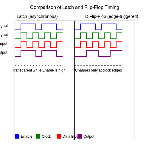
5.2 Power Consumption and Performance
The analysis of power consumption and performance in flip-flops and latches is critical for designing efficient digital circuits. These components are the fundamental building blocks that dictate not only the speed of a circuit but also its energy efficiency. Understanding the interplay between performance metrics and power consumption helps engineers make informed decisions in various applications, from microprocessors to memory devices.
Power Consumption in Flip-Flops and Latches
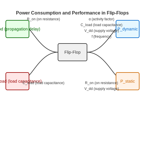
Flip-flops and latches consume power in two primary modes: dynamic and static. Dynamic power is consumed when the device is switching states and is affected by the switching frequency, the output load capacitance, and supply voltage.
The dynamic power consumption, P_dynamic, can be expressed mathematically as:
Where:
- α = switching activity factor, representing the proportion of flip-flops that switch in one clock cycle.
- C_load = load capacitance at the output.
- V_dd = supply voltage.
- f = switching frequency.
Static power, on the other hand, is consumed due to leakage currents when the flip-flop is not switching. It is crucial, particularly in low-power and portable designs, where battery life is paramount.
Performance Metrics
Performance in flip-flops and latches is typically evaluated in terms of speed (propagation delay) and area. The propagation delay, t_pd, is the time taken for an input change to produce a corresponding output change. This parameter can be influenced by several factors, including:
- The chosen technology (CMOS, BiCMOS, etc.)
- Transistor sizing
- Load capacitance and interconnect delays.
The propagation delay can often be modeled as:
Where R_on is the on-resistance of the transistors when they are conducting. The performance can, thus, be enhanced by minimizing load capacitance and choosing optimal transistor sizes based on load conditions.
Real-World Applications
In practical applications, power and performance are often at odds, leading to the need for trade-offs. For example, in low-power designs for wearable technologies, engineers may opt for slower flip-flops to reduce power consumption, ensuring longer battery life.
Conversely, in high-speed designs, such as those found in modern processors, minimizing propagation delay is crucial. Techniques such as voltage scaling, clock gating, or the use of please-hold times can effectively balance the needs for both performance and power efficiency.
As technology evolves, such as with new materials or circuit layouts (e.g., FinFETs), the methods for optimizing these parameters continue to advance, making this a vibrant area of research and development.
5.3 Simulation and Testing Techniques
Simulation and testing techniques are essential in the development process of flip-flops and latches, allowing engineers and researchers to validate designs before deployment. As digital systems become increasingly complex, the ability to verify the functionality and performance of these memory devices through simulations is crucial.
Understanding the Need for Simulation
The behavior of flip-flops and latches under various conditions can be intricate, depending heavily on timing, input conditions, and external environment factors. Simulation tools enable designers to assess performance metrics such as propagation delay, setup time, and hold time. These parameters are critical for ensuring that a design meets the desired operational specifications.
Types of Simulation Techniques
Several simulation techniques exist, each catering to a different aspect of flip-flop and latch design. The most prevalent methods include:
- Behavioral Simulation: This approach uses high-level models of logic and timing to predict the circuit's behavior without delving into lower-level transistor operations.
- Functional Simulation: Focuses on verifying the logical correctness of a design, ensuring that all desired states and transitions occur as planned.
- Timing Simulation: Addresses the timing aspects of circuits. It calculates the transition delays and examines impacts of varying input signals on output timings.
- Monte Carlo Simulation: Utilizes statistical methods to account for variations in manufacturing processes, which can significantly influence the performance of digital memory devices.
Tools and Environments for Simulation
A variety of simulation tools are available that support the development of flip-flops and latches:
- SPICE: Widely used in the field of electronics, SPICE (Simulation Program with Integrated Circuit Emphasis) allows engineers to simulate the electrical characteristics of circuits.
- VHDL/Verilog Simulation Tools: These hardware description languages (HDLs) enable behavioral and structural modelling of digital circuits. Tools like ModelSim and Vivado provide comprehensive simulation capabilities tailored to flip-flops and latches.
- MATLAB/Simulink: These environments allow for system-level simulations and can integrate various components seamlessly, offering users the ability to model timing and performance aspects accurately.
Implementing Simulation in Design Workflow
Incorporating simulations effectively into the design workflow necessitates a structured approach:
- Define the specifications and requirements of the flip-flops and latches.
- Develop a behavioral model using HDL or a similar language to encapsulate the behavior of multiple state changes.
- Run functional simulations to validate the logic against the requirements.
- Perform timing simulations to evaluate the circuit’s performance under real-world conditions.
- Iterate the design based on findings from simulations, ensuring compliance with timing and functionality specifications.
Testing Techniques
Once the design has been validated through simulation, practical testing becomes crucial. Various testing techniques can be employed to ensure reliability and robustness:
- Boundary Scan Testing: Utilizes a standardized method to test interconnection between integrated circuits.
- Functional Testing: Involves applying inputs to the memory devices and checking the outputs to ensure they meet expected results.
- Temperature and Voltage Stress Testing: Assesses the performance limits of flip-flops and latches under extreme conditions, critical for applications in harsh environments.
Conclusion
Flipping the electronic world into a state of reliability and efficiency hinges on the effective use of simulation and testing techniques. By understanding the tools and methods available, engineers can confidently validate their flip-flop and latch designs, leading to successful implementation in complex digital systems.
6. Integrated Circuit Implementations
6.1 Integrated Circuit Implementations
Flip-flops and latches are pivotal components in digital electronics, serving as fundamental storage elements in sequential circuits. The evolution of these devices from discrete components to integrated circuits (ICs) has significantly revolutionized how we implement memory and control functions in electronic designs. Integrated circuit implementations capitalize on high density, reduced power consumption, and improved reliability, propelling innovations in everything from consumer electronics to complex computer systems.
When we dive into the realm of integrated flip-flops and latches, we typically encounter several standard configurations such as SR, D, JK, and T flip-flops, each tailored to accommodate various functional requirements. The most common implementations utilize bipolar junction transistors (BJTs) or metal-oxide-semiconductor field-effect transistors (MOSFETs), with the latter being predominant in modern digital designs owing to their lower power requirements and greater speed performance.
Flip-Flops in Integrated Circuits
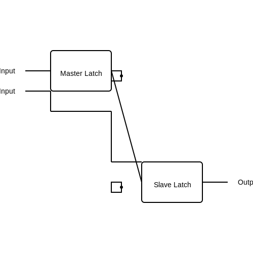
In an integrated circuit, a flip-flop can generally be implemented using a combination of logic gates arranged in a feedback configuration, asynchronous inputs for controlling states, and clock inputs for synchronization. For example, a D flip-flop, which is particularly favored for its simplicity and ease of use in edge-triggered scenarios, can be constructed using a master-slave configuration of two latches, with the input being sampled at clock edges.
The basic architecture of a D flip-flop can be represented using a schematic where:
- A data input (D) connects to the input of the first latch,
- The second latch outputs the stored value to the external circuit,
- Clock inputs control the timing of the state transition.
As you can see in the diagram below, the master latch captures the value of D at the triggering edge of the clock, while the slave latch holds the output steady until the next clock cycle:
Latches in Integrated Circuits
Latches, which differ from flip-flops in that they are level-triggered rather than edge-triggered, can also be integrated similarly. The SR and D latches are often created using NAND or NOR gates in a cross-coupled configuration. The propagation delay and setup time must be carefully considered in synchronous designs to prevent unwanted race conditions and ensure proper operation.
The integration of these components allows for compact design and scalability, as deploying a chip that contains numerous flip-flops and latches can vastly simplify the overall circuit design. Additionally, IC fabrication technologies, such as complementary metal-oxide-semiconductor (CMOS), combine both n-type and p-type transistors on a single substrate, helping optimize power efficiency while maintaining high performance.
Applications and Real-World Examples
The significance of integrated flip-flops and latches extends further into applications such as:
- Memory Storage: They serve in static RAM (SRAM) as the basic building blocks.
- State Machines: Flip-flops are integral in designing sequential circuits used in control applications.
- Frequency Division: T flip-flops are used in frequency dividers for clock management in digital systems.
As digital systems evolve, integrated flip-flops and latches continue to adapt, catering to higher speeds and lower power demands. Their implementation in the form of complex programmable logic devices (CPLDs) and field-programmable gate arrays (FPGAs) provides engineers with the flexibility to adapt designs in various applications ranging from automotive electronics to advanced telecommunications.
6.2 Emerging Technologies
The landscape of digital computing and data storage is evolving with the emergence of new technologies that seek to improve upon the traditional architectures of flip-flops and latches. These advances not only enhance performance but also incorporate innovative approaches to address current limitations, such as power consumption, speed, and integration density. In this subsection, we delve into promising technologies that are redefining the applications of sequential logic components.
Quantum Computing and Qubits
One of the most revolutionary aspects of emerging technologies lies in quantum computing, which utilizes qubits instead of classical bits. Unlike traditional flip-flops that can hold a state of either 0 or 1, qubits can exist in a state of superposition, allowing them to represent multiple states simultaneously. This fundamental shift can lead to extraordinary computational power for specific problems, such as cryptography, complex system simulations, and optimization tasks.
The implementation of qubits often leverages principles of quantum mechanics, with devices like superconducting circuits and trapped ions serving as platforms for qubit realization. For instance, superconducting qubits can be designed to form two-state systems where the states resemble a classical flip-flop but utilize quantum behavior to achieve faster processing capabilities.
Memristors: The Fourth Circuit Element
Another area of interest is the development of memristors, a novel type of passive circuit element that can store information without requiring continuous power. Memristors can be used to create non-volatile latches, maintaining their state (either high or low) even when power is disconnected. This characteristic closely aligns with the functionalities of traditional flip-flops, offering advantages in compactness, energy efficiency, and speed.
The unique ability of memristors to change their resistance based on the history of voltage and current can enable them to function as both memory and logic units, thus simplifying circuit design significantly. Applications of memristors are expanding, particularly in neuromorphic computing, where they emulate synapses in human brains, paving the way for intelligent computing systems.
Spintronics and Spin-Based Logic
Spintronics, or spin transport electronics, represent yet another emerging technology that utilizes the intrinsic spin of electrons in addition to their charge, potentially leading to faster and more efficient processing elements. Unlike conventional latches, spin-based logic devices could switch states much faster, combined with lower power requirements due to reduced energy dissipation during state changes.
Examples of spin-based devices include spinors and magnetic tunnel junctions (MTJs), where the spin orientation of electrons can represent logic states. This novel approach to manipulating electron spin has significant implications for future data storage solutions and rapid logic operations, thus enhancing computational efficiency.
Conclusion
As we forge ahead into the future of digital electronics, the incorporation of quantum computing, memristors, and spintronics represents a leap beyond traditional circuit designs. These emerging technologies promise not only to enhance performance metrics but also to reshape how we conceptualize computation itself. Understanding these advancements paves the way for innovation in engineering applications, creating a new pathway for reliable, efficient, and powerful electronic devices.
6.3 Comparison with Other Memory Elements
The realm of digital memory encompasses various elements, each serving distinct roles in the architecture of computer systems. In this subsection, we will explore how flip-flops and latches stack up against other memory types, such as SRAM (Static Random-Access Memory), DRAM (Dynamic Random-Access Memory), and ROM (Read-Only Memory). Understanding these comparisons is crucial for engineers and researchers when designing efficient and effective memory systems.Understanding Flip-Flops and Latches
Before delving into comparisons, it's imperative to establish a solid grasp of what flip-flops and latches are and their fundamental functioning. Both are bistable devices used to store binary data, and their operation is sensitive to the timing and control signals. A latch is level-triggered, meaning it maintains its output as long as the control signal is active. In contrast, a flip-flop is edge-triggered, changing its state only at the transition moments of a clock signal. The implementation choices for flip-flops and latches present distinct benefits and drawbacks: - Speed: Flip-flops can achieve higher operational speeds owing their edge-triggered nature allowing for synchronous data storage. - Complexity: Latches, while simpler, can introduce challenges in timing synchronization, particularly in larger designs requiring precise control.SRAM and Flip-Flops: A Natural Comparison
When contrasting flip-flops with SRAM, we see noteworthy similarities and differences. Both are used for storing data bits, with SRAM employing six transistors per cell to maintain its state without needing refresh cycles, unlike DRAM. However, SRAM is dynamic in its structure; it is faster and more reliable than flip-flops when employed for cache memory in CPU architectures: - Use Case: SRAM is widely utilized as cache memory due to its high speed, while flip-flops are employed primarily in sequential logic circuits where clock signals dictate data movement. While SRAM operates at the bit level, flip-flops can be cascaded to create registers, which can be used to build larger memory blocks. Despite this similarity in purpose, their architectures and operational conditions differ significantly.DRAM: A Different Approach
Dynamic Random-Access Memory (DRAM) employs a different operational principle compared to both flip-flops and latches. DRAM uses a single transistor and a capacitor to represent a bit of information: - Refresh Requirement: The key characteristic of DRAM is its need for periodic refresh cycles to maintain data integrity due to the leakage of charge. - Density and Cost: DRAM cells are more densely packed than flip-flops, making them cheaper for mass storage but slower when it comes to the access time. In many applications, particularly in personal computers, DRAM is the staple for expanding main memory, while flip-flops serve the purpose of controlling the flow of data – largely in digital circuits rather than large-scale memory applications.ROM: Stability with Trade-offs
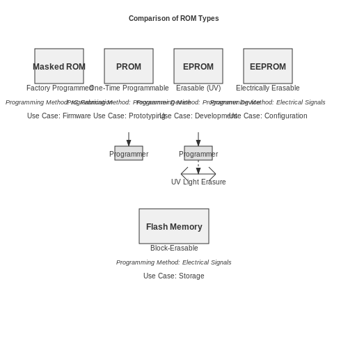
Read-Only Memory (ROM) is permanent storage, often utilized for firmware. It contrasts both flip-flops and latches due to its primary use case: - Non-volatility: ROM retains its contents even when power is removed, unlike latches and flip-flops which are volatile memory. - Application: ROM is crucial in boot processes of computers and embedded systems, providing a stable code execution environment. The primary trade-off with ROM is access speed versus programming flexibility. Whereas flip-flops allow for rapid data alteration through clock-controlled processes, ROM is slower and intended for immutable data.Real-World Applications and Practical Implications
Comparing these memory elements is not merely academic; it carries profound implications across digital system design: - Embedded Systems: Designers often utilize a combination of flip-flops for control logic, SRAM for cache, and DRAM for main memory to ensure optimal performance. - Data Integrity: Understanding the reliance on timing in flip-flops is crucial in designing circuits that minimize race conditions and glitches. In conclusion, while flip-flops and latches play vital roles in memory architecture, their capabilities differ significantly from SRAM, DRAM, and ROM. A comprehensive understanding of these differences is paramount for engineers and developers striving to create efficient systems tailored to their specific needs, maximizing performance while managing complexity and cost.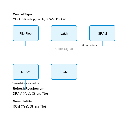
7. Books on Digital Electronics
7.1 Books on Digital Electronics
- Practical Electronics for Inventors by Paul Scherz — This comprehensive guide covers the necessary fundamentals of digital electronics, including in-depth sections on flip-flops, latches, logic gates, and timing. It blends theory with practical application, offering extensive exercises and real-world projects.
- Digital Design: Principles and Practices by John F. Wakerly — Focuses on both the pragmatic aspects of digital design and theoretical concepts. Readers will find detailed explanations of flip-flops and their integration into larger circuits, alongside CAD and HDL techniques.
- Digital Fundamentals by Thomas L. Floyd — A classic textbook that covers digital logic and latch circuits in great detail. Emphasizes the combination of theory and practical design, with a range of examples and problem-solving exercises.
- Digital Electronics: A Practical Approach with VHDL by William Kleitz — This book introduces VHDL alongside traditional digital theory, providing modern context for flip-flops and latches through simulation and actual experimental setups.
- Contemporary Logic Design by Randy H. Katz and Gaetano Borriello — Provides a hands-on approach to digital circuits, emphasizing logic design, including detailed discussions on synchronous sequential logic circuits like flip-flops and latches, with real-world case studies.
- Fundamentals of Digital Logic with VHDL Design by Stephen Brown and Zvonko Vranesic — Merges VHDL design with digital logic basics, providing an extensive overview of latches and flip-flops. Comes with practical exercises to enhance understanding and application.
- Electronic Principles by Albert Malvino — While traditionally an analog electronics text, this book includes essential chapters on digital logic principles, particularly emphasizing storage elements like flip-flops and memory cells.
7.2 Research Papers and Articles
- CMOS Latches and Flip-Flops Design Challenges — This paper from IEEE provides an in-depth exploration of design methodologies and challenges in creating CMOS-based flip-flops and latches. It includes performance metrics and their implications in modern integrated circuit design.
- Efficient Latch Design with Low Power Consumption — This IEEE article examines innovative designs aimed at reducing power consumption in latch circuits, thereby extending the lifetime and efficiency of electronic devices.
- Advancements in Flip-Flop Architectures for High-Speed Applications — ACM's paper discusses the recent advancements in flip-flop architectures that enhance speed performance, making them ideal for high-frequency applications.
- Latches and Flip-Flops in Microprocessor Systems: A Comprehensive Analysis — Sage Journals provide a thorough analysis of the role latches and flip-flops play in exotic microprocessor systems, detailing their impact on processing power and latency.
- The Role of Flip-Flops in Modern VLSI Systems — ScienceDirect offers insights into how flip-flops are utilized in Very-Large-Scale-Integration (VLSI) systems, emphasizing their critical function in high-density electronics.
- A Survey on State-of-the-Art Latches and Flip-Flops — This SpringerLink article surveys cutting-edge latch and flip-flop technologies, summarizing their application in modern digital systems and the advancements in low power, high speed, and robustness.
- Comparative Analysis of Flip-Flop Based Circuits in Digital Systems — Sage Journals provide a comparative analysis of various flip-flop based circuits, assessing their performance in different digital system configurations and their effect on overall circuit efficiency.
- Innovative Latch Designs for Nano-scaled Technologies — This research article by ScienceDirect investigates the design of latches tailored for Nano-scaled technologies, aiming to solve challenges related to leakage power and high-speed operation.
- The Future of Flip-Flops in Quantum Computing Environments — ACM explores the implications and potential adaptations of flip-flop circuits within quantum computing frameworks, discussing theories and experimental evidence related to quantum state control.
Subsection 7.3: Online Resources
- Electronics Tutorials: Flip-Flops — This comprehensive guide covers the basics of flip-flops, including S-R, J-K, D, and T types, with detailed diagrams and equivalent circuits.
- Texas Instruments: Fundamentals of Latches and Flip-Flops — A technical document that offers an in-depth exploration of latch and flip-flop types, functionalities, and applications in digital circuits.
- Guru99: Flip-Flop Types — An educational platform providing a straightforward explanation of different flip-flop configurations and how they are utilized in various digital applications.
- Analog Devices: Understanding Basic Flip-Flops and Latches Concepts — A tutorial that details the operating principles of flip-flops and latches, focusing on practical design considerations.
- CodeCogs: Flip-Flops — A platform offering mathematical and theoretical insights into flip-flop and latch operations with practical problem-solving examples.
- YouTube: Flip-Flops and Latches Tutorial — A video presentation that serves as a visual aid to understand the functionalities and applications of various flip-flop types in digital electronics.
- NPTEL: Digital Circuits and Systems — An advanced online course offering comprehensive learning material on digital circuits, with modules specifically focused on flip-flops and latches.
- CircuitsToday: Flip-Flop Types and Applications — A detailed article explaining the various types of flip-flops, their construction, working principles, and real-world applications.
- CMOS VLSI: Flip-Flops — An academic paper providing a thorough analysis of flip-flop circuits popularly used in CMOS VLSI design.