Applied Memory Devices
1. Types of Memory Devices
1.1 Types of Memory Devices
Memory devices form a crucial backbone in the field of electronics, playing pivotal roles across various applications, from everyday consumer electronics to advanced computing systems. The evolution of memory technology has given rise to a diverse array of memory types, each with specific characteristics and suitability for distinct applications. In this section, we will explore the various types of memory devices, their operational principles, and their practical applications.
Static and Dynamic Memory
At the most basic level, memory can be categorized into two primary types: Static RAM (SRAM) and Dynamic RAM (DRAM). SRAM uses bistable latching circuitry to store each bit, making it faster and more reliable than DRAM. It retains data as long as power is supplied and does not require periodic refreshing. These features make SRAM ideal for cache memory in processors.
In contrast, DRAM stores data in capacitors that must be refreshed thousands of times per second to maintain the data integrity. Despite being slower, DRAM is less expensive and more compact, making it the prevalent choice for main memory in computers and other devices.
Non-Volatile Memory
Non-volatile memory (NVM) retains data even when powered off. Among the most common types of NVM are:
- Flash Memory: This form of memory is widely used in USB drives and SSDs. It uses floating-gate transistors to store data. The ability to rewrite data in blocks makes flash particularly versatile.
- Read-Only Memory (ROM): ROM is used primarily for firmware storage. Unlike other types, its data cannot be modified or can be modified only with difficulty.
- Magnetoresistive RAM (MRAM): This newer technology combines the non-volatile nature of NVM with the speed of SRAM, utilizing magnetic states to store data.
Emerging Memory Technologies
The landscape is constantly evolving, with several emerging memory technologies promising substantial improvements in speed, endurance, and efficiency:
- Phase-Change Memory (PCM): PCM stores data by changing the state of a material between amorphous and crystalline forms, offering excellent potential for scalability and speed.
- Resistive RAM (ReRAM): This technology alters the resistance of a material to store data, boasting faster speed than DRAM and greater endurance compared to flash memory.
Practical Applications
The choice of memory device greatly influences the performance and functionality of electronic systems. For instance:
- Consumer Electronics: Smartphones and cameras utilize flash memory for storage due to its speed and form-factor advantages.
- High-Performance Computing: SRAM is essential for cache memory in CPUs, ensuring swift data access for computation-intensive applications.
- Embedded Systems: ROM and EEPROM are often employed in embedded systems due to their non-volatile nature, storing essential code and configuration settings.
In conclusion, the choice of memory technology not only affects device performance but also dictates the feasibility of certain applications. As we advance into a future where speed and efficiency are paramount, the development of new memory technologies will continue to play a central role in electronics engineering.
1.2 Characteristics of Memory
In the domain of applied memory devices, understanding the characteristics of memory is critical, as these properties define how memory systems can be utilized in practical applications. Memory characteristics dictate not just performance but also the underlying technology, impacting factors such as speed, capacity, and energy efficiency. This section delves into these fundamental aspects, helping advanced readers appreciate the nuances in memory behavior.Speed and Latency
Memory speed is primarily defined by two key metrics: access time and data transfer rate. Access time indicates how quickly a memory device can retrieve or store data, while data transfer rate reflects how much data can be moved in a given timeframe. To quantify access time, one often considers the timing parameters specific to memory types. For example, DRAM (Dynamic Random-Access Memory) typically has access times in the order of nanoseconds, making it much faster than traditional magnetic hard drives. In contrast, Flash memory, while slower than DRAM, provides decent performance for non-volatile storage, with access times in the range of microseconds. Latency is crucial in determining the responsiveness of memory. Low-latency memory, such as SRAM (Static Random-Access Memory), can greatly enhance the performance of applications requiring rapid data processing, such as in cache memory systems.Capacity and Density
Memory capacity is a direct function of the physical structure and technology employed in the memory device. Emerging technologies, like 3D NAND in Flash memories, have allowed for increased density, enabling higher data storage capabilities within compact physical spaces. The capacity can range from a few megabytes in older technologies to several terabytes in modern enterprise-grade SSDs. The concept of memory density also pertains to how closely packed memory cells can exist within a given area. Higher density allows for more data storage but can introduce complexities such as increased cross-talk and interference, which engineers must carefully manage during design.Volatility and Persistence
Another crucial characteristic of memory is whether it is volatile or non-volatile. Volatile memory, which requires power to maintain the stored information, includes types like DRAM and SRAM. In contrast, non-volatile memory retains data even when power is lost, typified by NAND Flash and magnetic storage devices. The choice between volatile and non-volatile memory is significant in system design. For instance, volatile memory is typically deployed where speed is paramount—like CPU caches—while non-volatile memory is essential for long-term data storage solutions.Energy Efficiency
Energy consumption is an increasingly vital characteristic, especially as data centers and consumer electronics pursue greener technologies. Memory devices are often rated for energy efficiency, illustrating how much power consumption correlates with performance. The implementation of low-power modes in DRAM, such as self-refresh to reduce idle energy consumption, points to practical applications in mobile and wearable devices that require extended battery life without sacrificing performance.Durability and Endurance
Durability and endurance characterize how long memory devices can operate effectively under typical usage conditions. For instance, Flash memory cells wear out after a finite number of write cycles, highlighting the importance of wear leveling techniques to extend lifespan. Similarly, the robustness of magnetic storage against physical shocks can be a decisive factor for applications in portable devices. Real-world considerations, such as environmental exposure and the demands of specific applications, further influence the selection of memory types based on their durability profiles.Conclusion
The multifaceted characteristics of memory technologies—speed, capacity, volatility, energy efficiency, and durability—play a pivotal role in the design and selection of memory devices for various applications. Understanding these characteristics equips engineers and researchers with the insights needed to drive innovations in memory technology and solutions tailored to specific needs.Thus, as we continue to advance into a data-driven future, the exploration and optimization of memory characteristics will remain at the forefront of technological development, influencing everything from hand-held devices to large-scale data centers.
1.3 Trends in Memory Technology
Memory technology has evolved remarkably over the past few decades, driven by the rising demand for faster, denser, and more energy-efficient memory solutions. This section discusses significant trends influencing the landscape of memory devices, with a focus on innovations that bridge theoretical principles and practical applications.The Shift Towards Non-Volatile Memory Technologies
As data storage requirements have surged exponentially, non-volatile memory (NVM) technologies have gained significant traction. Unlike traditional volatile memories such as DRAM, which require a constant power supply, NVM retains data even when powered off. Key NVM technologies include Flash memory, phase-change memory (PCM), and resistive random access memory (ReRAM). The shift toward NVM enhances durability and power efficiency, making it ideal for a new generation of devices ranging from smartphones to large-scale data centers. Phase-change memory operates on the principles of thermal energy-induced changes in the state of chalcogenide materials. By applying specific amounts of current, the material can rapidly switch between amorphous and crystalline states, corresponding to binary "0" and "1." Flash memory, meanwhile, utilizes floating-gate transistors to trap charges, representing stored data. These advancements present a path towards higher speed and greater data retention, aligning closely with the increasing pursuit of low-latency architectures.Integration of 3D Architectures
Another trend revolutionizing memory technology is the integration of three-dimensional (3D) architectures. Traditional memory architectures predominantly rely on planar structures, which face challenges related to space and power consumption as the sizes of memory chips decrease. 3D architectures stack memory cells vertically, allowing for higher densities without compromising performance. This stacking technique not only enhances density but also reduces latencies due to shorter interconnect lengths between layers. Technologies such as 3D NAND exemplify this trend, permitting manufacturers to produce flash memory chips that utilize vertical stacking of memory cells. The result is a significant improvement in both storage capacity and operational speed, addressing modern computational demands effectively.New Materials and Their Impact
Advancements in materials science continue to influence the trajectory of memory technology. The transition to new materials, such as two-dimensional (2D) materials like graphene and transition metal dichalcogenides (TMDs), is a promising area of research. These materials can exhibit unique electronic properties, enabling the development of memory devices that offer enhanced performance and new functionalities. For example, memory devices using TMDs have demonstrated potential for low-voltage operation and improved switching speeds. As research continues to evolve, the integration of these innovative materials presents opportunities for revolutionary shifts in memory technology that could lead to novel applications across various sectors.Artificial Intelligence and Memory Devices
The advent of artificial intelligence (AI) has also begun to shape the development of memory technologies. Traditional memory architectures may struggle to meet the demands of AI workloads due to their high throughput and large data volumes. The rise of neuromorphic computing systems, which mimic the human brain’s architecture, has propelled interest in memory devices that can process and store information in ways analogous to the neural connections in biological systems. Memristors—devices that remember the amount of charge that has previously flowed through them—are of particular interest in this area. These devices allow for in-memory computing, significantly reducing data transfer times and energy consumption. This integration of memory and processing capabilities is expected to drive further innovations in hardware designed for AI applications.Conclusion
In summary, the trends shaping memory technology reflect an intricate tapestry of innovations driven by the relentless pursuit of speed, efficiency, and capacity. As industries continue to demand enhanced data handling capabilities, the convergence of non-volatile memories, 3D architectures, new materials, and AI will redefine what is possible in memory device functionality and applicability. This ongoing evolution not only shapes the future of memory technology but also increasingly aligns it with the complex requirements of modern computational environments. As researchers, engineers, and manufacturers leverage these trends, we can expect to witness transformative advancements across numerous technological domains.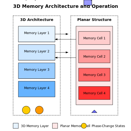
2. Static Random Access Memory (SRAM)
2.1 Static Random Access Memory (SRAM)
Static Random Access Memory (SRAM) stands as a cornerstone in the landscape of memory technology, revered for its speed and efficiency. Unlike its counterpart, Dynamic RAM (DRAM), which requires periodic refreshing, SRAM retains data bits in its memory as long as power is supplied, hence the term "static." This chapter delves into the operational principles, architecture, and practical significance of SRAM, empowering engineers and physicists with insights applicable in various high-performance environments.
Operational Principles and Architecture
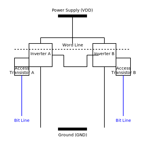
At its core, SRAM utilizes a series of bistable latching circuitry to store bits. Specifically, each bit of SRAM is stored in a flip-flop, which comprises several transistors arranged to create a latch. A typical SRAM cell generally uses six transistors, known as 6T SRAM, configured in such a manner that two cross-coupled inverters form the core of the cell, while additional transistors handle access control via a word line and bit lines.
To elucidate this, let's outline the mechanism:
- Storage Mechanism: The two cross-coupled inverters maintain the state of the cell. For example, if one inverter's output is high, the other's will be low, creating a stable state.
- Access Mechanism: When a specific word line is activated, the access transistors allow for read or write operations to occur with the bit lines.
Where \( V_{TH} \) represents the threshold voltage needed for the inverter to switch states, which is critical in determining the reliability of data retention.
Performance Characteristics
SRAM's resilience against data loss due to power fluctuations or transistor leakage renders it suitable for high-speed applications. Key characteristics include:
- Speed: SRAM significantly outpaces DRAM in data access speeds, making it ideal for cache memory in processors.
- Power Consumption: Although faster, SRAM has comparatively higher static power consumption, which is a critical consideration in battery-operated devices.
- Density: SRAM cells are larger than DRAM cells due to the additional transistors, which mandates a trade-off between speed and memory density.
Applications and Real-World Relevance
Due to its unique attributes, SRAM finds application in numerous fields:
- Cache Memory: Processor caches leverage SRAM to deliver quick access to frequently utilized data, thereby boosting the overall computational performance.
- Networking Equipment: Devices such as routers utilize SRAM to manage routing tables and buffers efficiently, ensuring rapid data transfer across networks.
- Embedded Systems: SRAM is widely implemented in embedded applications requiring fast data access, such as automotive control systems and medical devices.
Overall, SRAM continues to evolve, with innovations aimed at enhancing speed, reducing power consumption, and optimizing size, opening doors to new applications in the rapidly advancing fields of electronics and computing.
Conclusion
In conclusion, understanding the intricate workings of SRAM not only highlights its essential role in modern technology but also sets the stage for future innovations in memory devices. Familiarity with both its operational principles and practical applications equips engineers and researchers to harness its capabilities effectively.
2.2 Applications of SRAM
Static Random Access Memory (SRAM) is a pivotal technology in modern electronics, appreciated for its speed and efficiency. Unlike Dynamic RAM (DRAM), which requires periodic refreshing to maintain data, SRAM retains data bits in its memory as long as power is supplied. This fundamental difference manifests in various applications where speed, reliability, and power consumption are prioritized.
High-Performance Computing
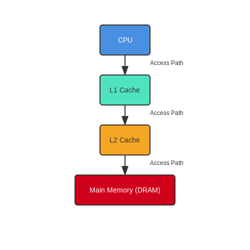
At the forefront, SRAM is extensively applied in high-performance computing (HPC). The architecture of supercomputers and data centers often incorporates SRAM in cache memory systems. Cache memory, located closer to the CPU than main memory, significantly reduces latency and improves processing speeds. For example, the L1 and L2 caches in processors commonly use SRAM due to its fast access time.
To understand the performance benefits, consider a multi-core processor with a hierarchical cache system. The CPU utilizes the fastest level of cache, which eliminates the delay associated with searching through slower main memory. This principle can be mathematically expressed in terms of access time:
Where:
- Ttotal is the total access time.
- TCPU is the time taken by the CPU to process instructions.
- Tcache is the access time for cache memory, which is significantly lower for SRAM.
- Tmemory is the access time for main memory (usually DRAM).
Communication Systems
In communication systems, SRAM plays a vital role in network routers and switches. These devices require high-speed data processing capabilities to manage data packets efficiently. SRAM is leveraged for storing routing information and immediate packet processing tasks, enhancing overall throughput. Further, its low power consumption aligns well with the requirements of portable devices and battery-operated systems.
Consider a router with a high-speed interface employing SRAM to quickly store and retrieve its routing tables. This allows for minimal latency in packet switching, critical for maintaining the integrity of real-time communications, such as voice over IP (VoIP) services.
Consumer Electronics
In the realm of consumer electronics, SRAM is often found in devices that demand rapid data access, such as smartphones, tablets, and gaming consoles. Here, it is typically used in short-term data caching, enabling swift application loading and multitasking capabilities.
For instance, modern gaming consoles employ SRAM to manage game state and facilitate seamless transitions between applications. This enhances user experience by reducing lag and ensuring that applications remain responsive during intense graphic processing scenarios. The dynamic interplay of speed and efficiency is essential in sustaining high frame rates and fluid graphics rendering.
Automotive Applications
Furthermore, with the rise of intelligent automotive systems, SRAM has started to find applications in automotive electronics. Systems such as advanced driver-assistance systems (ADAS) rely on quick data processing and low latency responses, where SRAM serves as an ideal candidate for temporary data storage. Whether it's managing sensor data or handling real-time computations for vehicle dynamics, SRAM's speed ensures that safety features react instantaneously.
In summary, SRAM embodies a crucial element in various fields where speed, reliability, and power efficiency intersect. From data centers to consumer gadgets and automotive technology, its impact is felt across the technological spectrum, enabling devices to perform at their peak potentials.
2.3 SRAM Design Considerations
Static Random Access Memory (SRAM) is a vital component in modern electronics, utilized extensively for cache memory in CPUs and as a high-speed storage solution in various digital devices. The design of SRAM cells is influenced by numerous considerations that can significantly impact performance, power consumption, and area utilization. This subsection explores key factors architects must account for when designing SRAM cells.
Understanding SRAM Cell Architecture
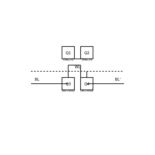
An SRAM cell typically consists of a bi-stable multivibrator, more specifically a flip-flop, which retains its state indefinitely as long as power is supplied. A basic SRAM cell usually employs six transistors (6T) for implementing the memory cell, achieving high data stability and low noise margins. The structure includes two cross-coupled inverters and two access transistors connected to the bit lines for reading and writing data.
In Figure 1, the configuration of a 6T SRAM cell is illustrated. The transistors Q1 and Q2 form a latch, while Q3 and Q4 serve as access transistors controlled by the word line. This design effectively provides read and write functionalities.
Critical Design Considerations
When designing SRAM cells, several critical aspects must be evaluated:
- Cell Size and Density: The trade-off between the storage capacity of the SRAM cell and its physical size is pivotal. Compact designs increase density but can lead to higher coupling capacitance, which affects performance.
- Access Time: Access time, which refers to the time taken to read/write data, is crucial in high-performance applications. Designers need to optimize the pull-up and pull-down ratios and sizing of the transistors.
- Power Consumption: SRAM is volatile and requires constant power to maintain data. Techniques such as power gating are often employed to minimize static power during idle states.
- Stability and Noise Margin: SRAM cells must exhibit high stability against noise. Designing for sufficient noise margins ensures reliable operation under varying conditions.
- Temperature and Process Variability: With variations in manufacturing processes and temperature, ensuring consistent performance across these variables is critical. Careful calibration and compensation strategies can mitigate these effects.
- Read and Write Stability: The stability of the cell during read and write operations must be managed to prevent inadvertent data alteration. Employing techniques like enhanced bit-line sensing and control methodologies can bolster this aspect.
Real-World Applications of SRAM
SRAM's fast access times, low latency, and straightforward design make it essential in various applications, including:
- Cache Memory: Serving as the first memory layer in CPUs, SRAM acts as a cache that stores frequently accessed data, significantly speeding up processing tasks.
- Embedded Systems: SRAMS are widely used in embedded devices where speed and reliability are paramount, such as graphics processors and network chips.
- Networking Equipment: Routers and switches utilize SRAM for packet buffering, allowing quick data forwarding and reducing latency.
As SRAM technology continues to evolve, innovations in transistor structures, such as FinFETs and materials, are anticipated to enhance performance and scalability further, making it indispensable in future electronic architectures.
3. Dynamic Random Access Memory (DRAM)
3.1 Dynamic Random Access Memory (DRAM)
Dynamic Random Access Memory (DRAM) is a crucial component in modern computing, serving as the primary memory used in personal computers, servers, and a variety of electronic devices. Unlike static RAM (SRAM), which retains data bits in its memory as long as power is supplied, DRAM is volatile, meaning it loses its data when power is turned off. Yet, its advantage lies in its ability to store more data in a smaller physical space, a feature that has propelled its widespread adoption in applications where both capacity and cost-efficiency are paramount.
The Structure of DRAM Cells
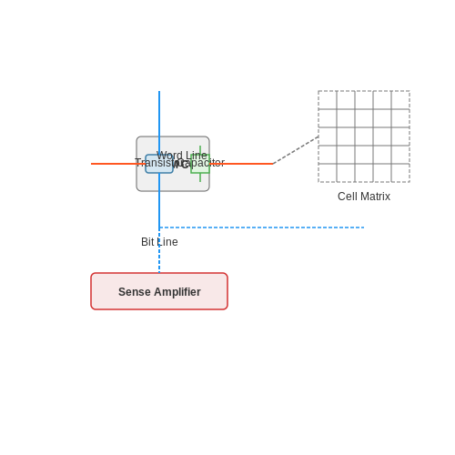
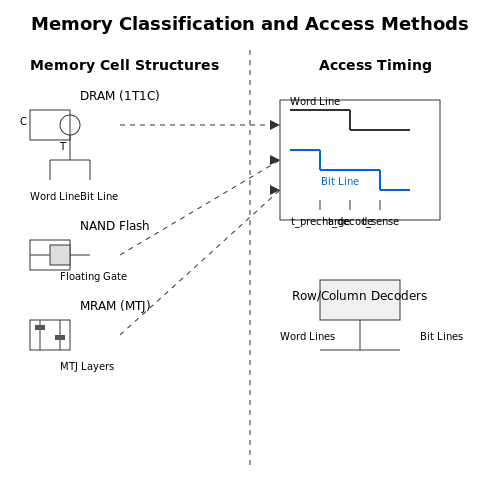
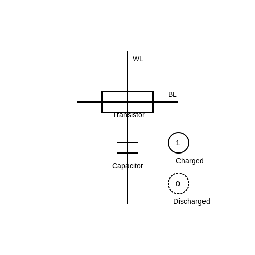
At the core of every DRAM chip is the memory cell, typically composed of a single transistor and a capacitor. The transistor acts as a switch that can either allow or block the flow of electricity, while the capacitor stores the electrical charge that represents a bit of data—a charged capacitor indicates a '1', and a discharged capacitor represents a '0'.
This simple structure leads to a fundamental limitation of DRAM; the capacitors leak charge, causing data to be lost over time. This necessitates a process known as refreshing, which involves periodically reading the charge in each capacitor and writing it back to prevent loss of data. The refreshing cycle is critical and must occur every few milliseconds, impacting the speed and efficiency of DRAM operations.
Operational Principles of DRAM
The operation of DRAM can be characterized by two phases: read and write.
Read Operation
During a read operation, the row address is selected, and the word line (WL) is energized. This enables the transistor connected to the selected memory cell, allowing the capacitor's charge to discharge onto a bit line (BL). The voltage across the bit line is then sensed and amplified, allowing the system to determine whether the stored bit is a '1' or '0'. Following this, the capacitor must be refreshed to restore its charge.
Write Operation
In a write operation, the process begins similarly with the row address selection and activation of the word line. However, instead of sensing the charge, the voltage on the bit line is set to reflect the data being written—either high (for '1') or low (for '0'). The transistor again becomes active, allowing the capacitor to charge or discharge accordingly. This operation is typically less time-consuming than reading, but it still necessitates careful timing to maintain data integrity.
The Refresh Mechanism
As previously mentioned, refreshing is a crucial aspect of DRAM functionality. The refresh operation can be performed in two ways: implicit and explicit refresh. Implicit refresh happens automatically as a part of normal memory operations, while explicit refresh requires specific commands from the controller. The timing and frequency of these refresh cycles directly impact the performance, with faster DDR (Double Data Rate) technologies optimizing the procedure to enhance efficiency.
Variations and Evolution of DRAM Technologies
Over the years, DRAM technology has evolved significantly, leading to various types that optimize speed, power consumption, and density. Notable variations include:
- Synchronous DRAM (SDRAM): Operates in sync with the system clock, improving performance over traditional asynchronous DRAM.
- DDR SDRAM: Transfers data on both the rising and falling edges of the clock cycle, effectively doubling the data rate.
- LPDDR (Low Power DDR): Designed specifically for mobile devices, it minimizes power consumption while maintaining performance.
Each advancement has brought DRAM closer to meeting the demands of modern applications, from high-speed computing to energy-efficient mobile platforms.
Applications and Impact
DRAM's role extends beyond merely functioning as memory in personal computers. Its applications encompass high-performance computing systems, servers that require large memory capacities, and mobile devices where power efficiency is critical. The advent of high-bandwidth memory (HBM), a type of DRAM that stacks multiple memory chips to provide exceptional bandwidth, is transforming data-intensive applications such as graphics processing, artificial intelligence, and big data analytics.
As we look ahead, the ongoing development in DRAM technology, driven by the demands of increasingly complex computing tasks, signals its enduring significance in the landscape of applied memory devices.
3.2 Memory Refresh Techniques
As we delve into the realm of applied memory devices, it becomes crucial to understand the concept of memory refresh techniques. Memory refresh is particularly relevant to dynamic random-access memory (DRAM) and certain types of non-volatile memories where data retention relies on maintaining charge states within capacitive cells. The primary challenge is that, over time, charge stored in these capacitors can leak away, leading to potential data loss. Thus, periodic refresh cycles are implemented to restore lost information, ensuring data integrity and functionality.
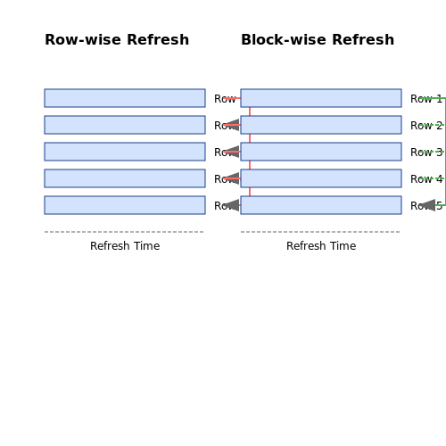
The two main categories of refresh techniques are row-wise and block-wise approaches. The row-wise technique refreshes one row at a time, sequentially accessing each row in the memory array, while the block-wise technique refreshes a grouped set of rows or an entire block of memory cells at once. Understanding these methods not only helps in designing reliable memory systems but also optimizes energy consumption, a vital aspect in battery-powered devices.
Row-wise Refresh
The row-wise refresh technique is often implemented in DRAM architectures. As the name suggests, this method entails reading a row of memory and then writing it back to ensure the integrity of the stored data. The refresh period—the time interval in which all rows must be refreshed—can typically be controlled through circuitry that synchronizes this operation.
-
The refreshing of a row can generally be expressed mathematically. Assuming there are n rows, the total time required for a complete refresh can be represented as:
$$ T_{refresh} = n \cdot T_{row} $$where Trow is the time taken to refresh each individual row.
- If the refresh period is less than the time needed for data retention, data loss is inevitable. This signifies the importance of establishing an adequate refresh rate.
Block-wise Refresh
In contrast, the block-wise refresh technique aggregates several rows for simultaneous refresh. This method increases the overall throughput and reduces latency, as multiple rows can be accessed and refreshed at once. One of the significant practical applications of block-wise refresh is in high-performance computing where memory access speed is critical.
This technique can optimize the refresh process particularly in systems that require swift access to substantial data volumes. The total time required for a block-wise refresh can be represented as:
Practical Considerations and Innovations
As technology advances, newer memory technologies like 3D NAND and emerging MRAM (Magnetoresistive RAM) are implementing innovative refresh strategies that significantly deviate from conventional approaches. The integration of on-chip logic for refreshing capabilities can potentially minimize refresh power consumption, which is critical in mobile applications where battery life is paramount. Furthermore, adaptive refresh techniques that tailor refresh rates based on access patterns are increasingly being adopted in modern memory systems.
Overall, developing efficient memory refresh techniques is imperative for maintaining data integrity in dynamic memory systems, optimizing energy consumption, and ensuring the overall functionality of memory devices in real-world applications ranging from consumer electronics to enterprise servers.
3.3 DRAM Performance Factors
Dynamic Random Access Memory (DRAM) is a critical component in modern computing systems, offering a balance between speed, density, and cost. Understanding its performance factors is essential for optimizing system design and enhancing overall efficiency. Performance in DRAM can be influenced by several key parameters, which include access time, bandwidth, latency, power consumption, and density. By carefully evaluating these factors, engineers can better tailor memory solutions to meet the demands of specific applications.
Access Time
Access time, often characterized as the time taken to read or write data in a memory cell, significantly affects DRAM performance. The access time is typically divided into random access time and sequential access time. Random access time is crucial for applications requiring frequent updates and quick read/write cycles, while sequential access time may be more relevant in streaming data scenarios.
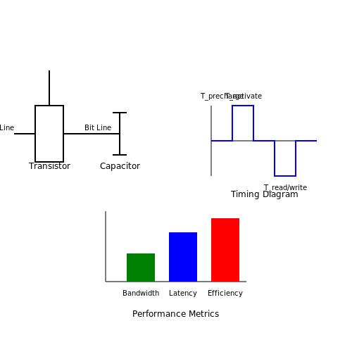
The access time can be mathematically quantified and is closely tied to the internal architecture of DRAM. Modern DRAM cells consist of a capacitor and a transistor. The capacitor holds the charge representing a binary state, while the transistor acts as a switch. The charging and discharging of these capacitors determine the speed at which data can be accessed. The equation governing the access time can be expressed as:
Here, \( T_{precharge} \) is the time taken to prepare a row of cells for reading or writing, \( T_{activate} \) denotes the time to activate the desired row, and \( T_{read/write} \) represents the time to perform the read or write operation. Together, these components form the total access time, highlighting the intertwined relationships between various operations within DRAM.
Bandwidth
Bandwidth in DRAM indicates the rate at which data can be read from or written to the memory. It is typically measured in megabytes per second (MB/s) or gigabytes per second (GB/s) and directly relates to the internal data bus width and clock frequency. A wider data bus allows multiple bits to be transferred simultaneously, thereby increasing the bandwidth. The relationship can be represented as:
As applications demand higher data throughput—particularly in fields such as machine learning, gaming, and data analytics—optimizing bandwidth becomes a critical factor in DRAM design. Advanced DRAM architectures like DDR (Double Data Rate) further enhance bandwidth by transferring data on both edges of the clock cycle.
Latency
Latency, the delay between the initiation of a read or write command and the actual data transfer, remains a major concern in DRAM performance. Latency can be categorized as row access latency or column access latency. Factors contributing to latency include the physical layout of memory cells, the design of the control circuitry, and the operational state of the memory (e.g., whether it is activated or precharged).
Reducing latency often involves architectural refinements such as bank interleaving, which allows multiple banks of memory to be accessed simultaneously, thus enabling overlapping operations and minimizing idle periods during memory transactions.
Power Consumption
Power consumption in DRAM is not merely a matter of performing computations; it also involves energy efficiency, particularly for mobile and embedded systems. There are three primary states where power consumption needs to be analyzed: idle, active, and refresh. The refresh operation, which is necessary to maintain data integrity by recharging the memory cells periodically, introduces significant energy overhead.
The power consumed during operation can be expressed as:
To enhance efficiency, manufacturers are developing low-power DRAM variants specifically designed for energy-sensitive applications, such as DRAM with reduced refresh rates or selective refresh patterns targeting only rows that have been accessed.
Density
Finally, memory density refers to the amount of data stored per unit area on the chip. Compact memory cells designed with smaller feature sizes allow for increased density, but this poses challenges, particularly regarding interference and thermal effects among adjacent cells. Balancing density with performance metrics ensures that the DRAM can satisfy both storage capacity and speed requirements.
In conclusion, understanding the performance factors associated with DRAM is crucial for designing cutting-edge memory solutions. As the push for faster, more efficient memory continues in technological sectors, ongoing research and innovation will play pivotal roles in shaping the future landscape of memory devices.
4. Flash Memory Technologies
4.1 Flash Memory Technologies
Flash memory technologies have transformed data storage across a multitude of applications, enabling agile computing environments and mobile devices. The evolution of flash memory has progressed through various generations, each pushing the limits of speed, capacity, and efficiency. In this section, we will explore the underlying principles, structures, and advancements in flash memory technology, focusing particularly on its operational characteristics and practical applications.
Fundamentals of Flash Memory
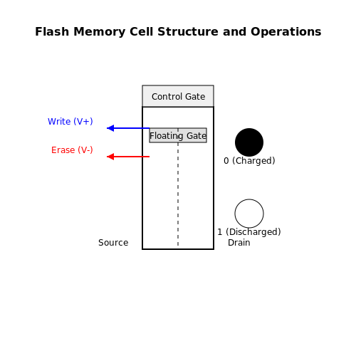
Flash memory is a type of non-volatile storage that retains data without needing a continuous power supply. It is primarily composed of floating-gate transistors, which store electrical charge to represent binary data. The key types of flash memory are:
- Single-Level Cell (SLC): Stores one bit of data per cell, offering superior speed and endurance.
- Multi-Level Cell (MLC): Stores two bits per cell, providing higher density but reduced performance and durability.
- Triple-Level Cell (TLC): Stores three bits, further increasing capacity at the expense of speed and reliability.
- Quad-Level Cell (QLC): Stores four bits per cell, maximizing storage density but having the lowest performance and longevity.
Each type has its unique advantages and limitations, making them suitable for different applications ranging from consumer electronics to enterprise data centers.
Operational Mechanisms
Understanding the operation of flash memory requires familiarity with two fundamental processes: writes and erases. In a write operation, electrons are injected into the floating gate of a transistor by applying a gate voltage, altering the cell's charge state and thus encoding a bit of information. Conversely, during an erase operation, the voltage is applied to drain the electrons out of the floating gate, resetting the bit.
The efficiency of these processes is influenced by the structure of the flash memory cells. For instance, the adoption of 3D NAND technology allows for vertical stacking of memory cells, significantly increasing storage density while maintaining speed and durability. The rise of this technology has addressed the scaling limits faced by traditional planar NAND cells.
Challenges and Innovations
Despite its widespread usage, flash memory is not without challenges. Key issues include write endurance, which refers to the limited number of program-erase cycles each cell can endure. Innovations such as wear leveling algorithms and error correction code (ECC) have been deployed to mitigate these issues, extending the operational lifespan of flash devices.
Moreover, the development of Multi-Die Packages allows manufacturers to combine multiple chips into a single package, further enhancing performance and efficiency for high-capacity applications.
Real-World Applications
Flash memory is prevalent in various applications, including:
- Consumer Electronics: Used in smartphones, tablets, and USB drives, leveraging SLC or TLC for balance between performance and cost.
- Enterprise Storage Solutions: MLC and SLC options dominate SSDs, providing fast data access speeds crucial for data centers and cloud computing.
- Automotive Systems: As vehicles become more connected, flash memory is vital for data logging, navigation systems, and infotainment units.
With increasing demands for faster and more reliable storage solutions, ongoing research and development in flash memory technology continue to yield innovative approaches that enhance performance, reliability, and cost-effectiveness.
In this equation, \( Q \) represents the electric charge stored in the floating gate, \( C \) is the capacitance of the gate, and \( V \) is the voltage applied. Understanding this relation aids in optimizing the design and efficiency of flash memory cells.
4.2 Phase-Change Memory (PCM)
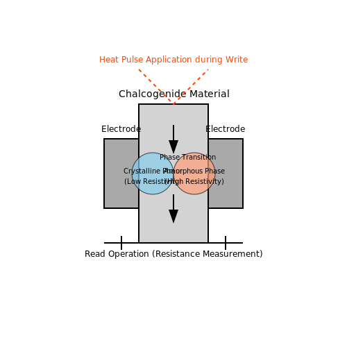
Phase-Change Memory (PCM) is an innovative non-volatile memory technology that utilizes the unique properties of certain chalcogenide materials to store information. The principle behind PCM lies in the ability of these materials to switch between two distinct phases: an amorphous phase that represents a logical '0' and a crystalline phase corresponding to a logical '1'. This phase transition is induced by the application of heat generated through electrical current, a characteristic that differentiates PCM from other memory technologies. The fundamental understanding of PCM begins with the behavior of chalcogenides, specifically their ability to undergo rapid and reversible phase changes. When a current is applied, localized heating results in the material transitioning from its crystalline state to an amorphous state, and vice versa when the heat is removed. The switching speed and efficiency of PCM make it an attractive alternative to traditional flash memory, especially given its potential for higher endurance and greater data retention.Operational Mechanism
The operational mechanism of PCM is predicated on thermal dynamics and materials science. The thermal energy required to induce a phase change in a material can be quantified using the specific heat capacity \(C\) and the temperature difference \(\Delta T\) through the equation:Advantages and Challenges
One of the substantial advantages of PCM over conventional Flash Memory is its scalability. PCM can potentially overcome the limitations related to charge trapping that hinder the scaling of Flash technology. Furthermore, PCM offers faster read and write speeds, coupled with a significantly higher number of write/erase cycles. While Flash typically allows for around 10,000 to 100,000 cycles, PCM can achieve upwards of 10^12 cycles, positioning it favorably for endurance-critical applications. However, PCM is not without challenges. The power consumption during write operations can be relatively high, and the transition time between states can vary based on the temperature and material composition. Additionally, integrating PCM into existing semiconductor fabrication processes poses logistical hurdles, requiring novel approaches to achieve compatibility with conventional silicon-based technologies.Real-world Applications
PCM technology is quickly gaining traction, finding its way into diverse applications ranging from high-performance computing to consumer electronics. Key applications include:- Cache Memory: Utilizing PCM as cache memory can greatly enhance system performance due to its speed and endurance advantages.
- Storage Class Memory: Emerging as a possible replacement for DRAM and Flash, PCM can bridge the speed gap between memory types.
- Embedded Systems: In embedded devices, PCM offers robust data retention alongside energy efficiency, making it ideal for mobile applications.
4.3 Emerging Non-Volatile Memory Solutions
As the drive for increased data retention and enhanced performance in electronic devices continues, emerging non-volatile memory (NVM) solutions showcase a blend of innovation and practicality. This section delves into the forefront of NVM technologies, particularly highlighting their potential applications in modern computing and data storage systems.Introduction to Emerging NVM Technologies
Non-volatile memories, unlike traditional volatile counterparts such as SRAM and DRAM, retain information even when powered off. The advancements in NVM solutions revolve around speed, endurance, and scalability, addressing the demands of the rapidly evolving digital landscape. Among the prominent candidates emerging in this domain are:- Phase Change Memory (PCM): Exploits the unique characteristics of phase-change materials, allowing rapid switching between crystalline and amorphous states.
- Spin-Transfer Torque Magnetic RAM (STT-MRAM): Uses spin-polarized currents to manipulate magnetic states, allowing for faster access times and lower power consumption.
- Resistive RAM (ReRAM): Leverages resistance switching in metal oxides, showcasing high density and compatibility with existing CMOS technology.
- Flash Memory Trends: New developments in flash technology, such as 3D NAND, enhance the capacity and speed of traditional flash storage.
Phase Change Memory (PCM)
Phase Change Memory (PCM) utilizes materials that can switch between two distinct states: amorphous (high resistance) and crystalline (low resistance). This phenomenon allows PCM to store binary data efficiently. Operating on the principle of thermal energy, PCM can read and write data at speeds comparable to those of DRAM. However, a critical advantage is its non-volatility, retaining its state even when power is removed. Recent developments have minimized the programming time required, pushing it further into the arena of mainstream usage. One of the most compelling applications for PCM is in future computing architectures, especially as a potential replacement for flash memory in consumer devices due to its faster read/write cycles.Mathematical Underpinnings
The energy efficiency of PCM can be quantified. The energy per bit ($$E_{bit}$$) required for phase transitions can be expressed as:Spin-Transfer Torque Magnetic RAM (STT-MRAM)
Spin-Transfer Torque Magnetic RAM (STT-MRAM) combines the principles of magnetic storage with the simplicity of semiconductor technology. Utilizing the spin of electrons, STT-MRAM achieves faster data writing compared to traditional magnetic RAM systems. STT-MRAM is particularly advantageous in scenarios where speed and energy efficiency are paramount, such as in real-time applications like mobile devices and servers. The endurance of STT-MRAM, exceeding that of flash memory, establishes its credibility in high-frequency applications.Resistive RAM (ReRAM)
Resistive RAM (ReRAM) offers high-density storage capabilities and fast switching speeds. By utilizing the resistance state of a material, ReRAM can achieve lower power consumption while maintaining data integrity through a greater number of write cycles. The unique architecture of ReRAM enables its integration with existing semiconductor fabrication technologies, thus paving its way into both consumer applications, such as SSDs, and enterprise solutions requiring high data throughput.Future Directions and Applications
The evolution of NVM technologies signals a dramatic shift in how we approach data storage and speed hierarchies in computing systems. Research into hybrid memory solutions that combine the strengths of these emerging technologies is ongoing, presenting opportunities to vastly improve performance while reducing costs. Practical implementations can range from enhancing mobile devices with faster app loading times to advancing cloud computing infrastructure with more efficient data centers equipped with robust, energy-efficient memory solutions. The integration of these technologies will also likely influence the development of new architectures, potentially replacing traditional memory hierarchies. This transformation can lead to more compact designs in electronic devices, balancing size and efficiency. In summary, the ongoing research and market interest in emerging non-volatile memory solutions promise not only to overcome the limitations of current memory technologies but also to revolutionize data handling in numerous applications that rely heavily on swift and reliable access to information.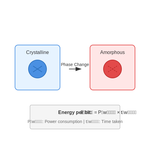
5. Read-Only Memory (ROM) Variants
5.1 Read-Only Memory (ROM) Variants
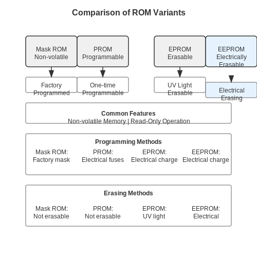
Read-Only Memory (ROM) is a type of non-volatile storage that is critical for storing firmware and software that does not change during the normal operation of a device. Unlike volatile memory such as RAM, ROM retains its contents even when powered off. Various ROM variants have implications across different applications, significantly impacting the performance and functionality of electronic devices.
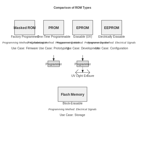
In this subsection, we explore some common ROM variants: Mask ROM, Programmable ROM (PROM), Erasable Programmable ROM (EPROM), and Electrically Erasable Programmable ROM (EEPROM). Each of these has unique characteristics that cater to specific requirements in memory usage, programming flexibility, and data retention.
Mask ROM
Mask ROM is the oldest type of ROM. Burned into the circuit during the manufacturing process, it cannot be reprogrammed. Its primary advantage is that it provides very rapid access times, making it suitable for applications like embedded systems in consumer electronics. However, the lack of reprogrammability makes it inflexible, as any changes require a new manufacturing process.
Programmable ROM (PROM)
Promotional ROM, or PROM, is the first type of ROM that can be programmed by the user. Once programmed, it retains the data like a traditional ROM. The programming process involves blowing fuses within the chip with a high voltage, effectively creating a link between the memory cells. This adaptability makes PROM suited for applications that need a one-time programmable solution, although it lacks the multi-write capability.
Erasable Programmable ROM (EPROM)
Next is EPROM, which enhances flexibility further by allowing the chip to be erased using ultraviolet light. This process removes the previous data, making it possible to reprogram the chip. The typical application of EPROM covers scenarios where multiple updates to firmware are beneficial, such as in early computing systems. However, it must be physically removed from the device for reprogramming, which can be a disadvantage in some designs.
Electrically Erasable Programmable ROM (EEPROM)
EEPROM is a step forward in convenience, allowing data to be erased and reprogrammed electrically, eliminating the need for removal from its circuit. This feature makes EEPROM widely applicable, especially in applications where frequent updates are necessary, such as in BIOS chips in computers. The trade-off is typically longer rewriting times compared to older ROM types.
As technology progresses, ROM variants are evolving. Flash memory, a specialized form of EEPROM, exemplifies this transition with improved speed and efficiency, enabling extensive use in USB drives and solid-state drives (SSDs).
In summary, ROM variants, with their distinct characteristics, serve critical roles in numerous applications across a variety of electronic devices. Their development reflects the evolving demands for speed, efficiency, storage, and adaptability in modern technology.
5.2 Cache Memory Design
Cache memory plays a critical role in augmenting the performance of modern computing systems by acting as a buffer between the high-speed CPU and the slower main memory (RAM). Through sophisticated design, cache memory reduces latency and increases data access speed, which is vital for applications that demand high performance, such as video processing, gaming, and large-scale scientific computations. The effectiveness of cache memory design hinges on three primary attributes: hierarchy, size, and associativity. Each attribute contributes uniquely to the overall efficacy of a caching strategy, which we will explore in detail.Cache Hierarchy
One of the fundamental tenets of cache memory design is the hierarchical structure. Generally, modern systems implement a multi-level cache hierarchy, typically consisting of L1, L2, and L3 caches. - L1 Cache: This is the smallest and fastest cache located closest to the CPU cores. It is usually split into two parts, one for data and one for instructions, allowing simultaneous access and minimizing latency. - L2 Cache: Slightly larger and slower than L1, the L2 cache serves as an intermediary to fetch data not found in L1. Its larger size aids in storing more extensive datasets at higher speeds than main memory. - L3 Cache: Shared among multiple CPU cores, L3 is slower than L1 and L2 but significantly larger. It attempts to reduce the frequency of RAM access by providing a last-resort data repository. The hierarchical arrangement minimizes average access time, with most data hits happening in the faster levels of the cache.Cache Size and Impact on Performance
The size of cache memory has a direct impact on performance metrics. A larger cache can store more data, theoretically leading to fewer cache misses. However, size also influences access speed and complexity. There are several factors to consider regarding cache size: - Diminishing Returns: Beyond a certain size, increases in cache capacity yield diminishing returns. The likelihood of finding frequently accessed data, known as temporal locality, can be fully exploited with a reasonably sized L1 and L2 cache. - Cost and Complexity: Larger caches are more expensive, more complex to design, and can lead to longer access times due to increased search depths. - Working Set Size: The working set concept describes the active data that a program uses at any given time. Understanding a program's working set size can help determine the optimal cache size.Associativity
Associativity determines how cache lines are mapped to cache slots, and it profoundly affects both performance and implementation complexity. - Direct Mapped Cache: Each block of main memory maps to exactly one cache line. While it is fast and simple to implement, it can suffer from conflict misses when multiple addresses map to a single line. - Fully Associative Cache: Any block can be placed in any cache line. This approach maximizes hit rates but introduces complexity due to the need for a more sophisticated replacement policy. - Set Associative Cache: Combining the two, set associative caches allow each block to be mapped to one of several lines, striking a balance between the simplicity of direct mapping and the flexibility of fully associative caches. Set associativity is commonly denoted as “n-way”, where n specifies how many lines can be accessed in a set at one time. The choice of associativity is often influenced by the nature of the workload and the performance desired.Performance Metrics and Evaluation
The performance of cache memory can be evaluated using several metrics: - Hit Rate: The percentage of memory accesses that are served directly from the cache. - Miss Rate: The percentage of memory accesses that do not find the required data in the cache. - Average Memory Access Time (AMAT): This can be calculated using the formula: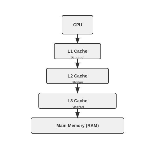
5.3 Memory in Embedded Systems
Embedded systems, characterized by their dedicated function within a larger mechanical or electrical system, rely heavily on different types of memory to perform efficiently. The design and architecture of memory within these systems is crucial as it directly impacts performance, power consumption, and overall system capabilities. Understanding the various memory types used in embedded systems aids in selecting appropriate memory solutions tailored for specific applications, thereby enhancing system performance.
Types of Memory in Embedded Systems
There are several types of memory utilized in embedded systems, each offering unique advantages and characteristics suited to specific applications. The primary categories include:
- Volatile Memory: This category includes RAM (Random Access Memory) such as SRAM (Static RAM) and DRAM (Dynamic RAM). Volatile memory is fast and used for temporary data storage during operation.
- Non-volatile Memory: Types of memory such as Flash, EEPROM (Electrically Erasable Programmable Read-Only Memory), and FRAM (Ferroelectric RAM) fall under this category. Non-volatile memory retains information even when the power is off, making it ideal for firmware storage or application settings.
- Cache Memory: A smaller, faster memory type that temporarily stores copies of frequently accessed data from main memory, significantly enhancing the speed of data retrieval.
Design Considerations
When choosing memory for embedded systems, several design considerations must be taken into account:
- Access Speed: The speed of memory access can greatly affect the overall performance of the embedded system. For example, SRAM is faster than DRAM but also more expensive and has lower density.
- Power Consumption: In battery-operated devices, power efficiency of memory types becomes critical. Flash memory, for instance, consumes less power during operation compared to volatile memory types.
- Endurance and Reliability: Non-volatile memory options vary in their write/erase cycle limits. For instance, Flash memory may have limited write cycles compared to FRAM, which boasts higher endurance.
- Cost: The cost-effectiveness of memory types plays a critical role, as memory can often constitute a significant portion of the overall manufacturing cost in embedded systems.
Practical Applications
The combination of these memory types allows for versatility in the field of embedded systems. Real-world applications include:
- IoT Devices: Internet of Things (IoT) devices often utilize Flash and SRAM for firmware and data storage due to their compact design and non-volatile characteristics.
- Consumer Electronics: Products like smart TVs and gaming consoles leverage a mix of RAM for operational speed and Flash memory for firmware updates.
- Automotive Systems: Modern vehicles integrate various embedded systems for controlling everything from engine management to infotainment, requiring both fast and reliable memory solutions.
Future Trends
As embedded systems evolve, the need for adaptable and efficient memory solutions increases. Emerging technologies such as 3D NAND and memristor-based storage solutions are paving the way for future developments. These innovations focus on optimizing memory density, speed, and energy efficiency, catering to the ever-growing demands of modern embedded applications.
In summary, understanding the types of memory used in embedded systems, their characteristics, and design considerations is paramount for engineers and developers. Increased performance, reduced costs, and enhanced reliability are keys to successful embedded systems design.
6. 3D Memory Structures
6.1 3D Memory Structures
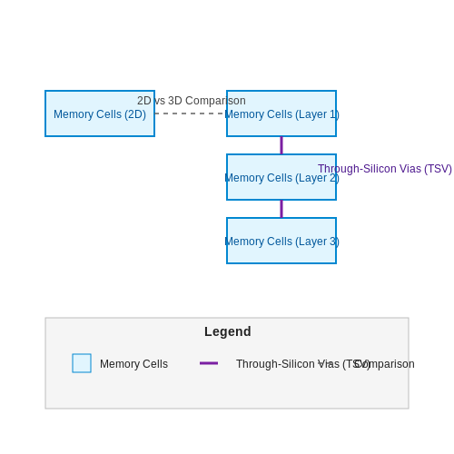
The evolution of memory technology has been driven by the need for higher density, improved performance, and reduced power consumption. One of the pivotal advancements in this domain is the advent of 3D memory structures. Unlike traditional 2D memory layout, where memory cells are spread out in a single layer, 3D structures allow memory cells to be stacked vertically, dramatically increasing storage capacity and performance efficiency.
The concept of 3D memory is not new; it was first introduced in early 2000s with the development of 3D NAND Flash. By employing stacking technology, manufacturers can overcome the limitations imposed by the shrinking process of planar transistors. However, the transition from 2D to 3D structures in memory devices has unlocked significant potential for future developments.
Understanding 3D Memory Architecture
At its core, a 3D memory structure consists of multiple layers of memory cells connected through vertical conduits known as through-silicon vias (TSVs). This architectural design offers numerous advantages:
- Increased Density: By stacking cells vertically, it is possible to significantly increase the number of bits per unit area, making more efficient use of the silicon wafer.
- Reduction in Latency: The vertical interconnections decrease the distance signals must travel, significantly reducing the latency associated with memory access.
- Power Efficiency: 3D structures reduce the capacitance and resistance of connections, resulting in lower power consumption compared to 2D alternatives.
The Fabrication Process
The fabrication of 3D memory involves several critical steps, often including:
- Layer Deposition: Using techniques such as chemical vapor deposition (CVD), layers of dielectric and conductive materials are deposited to form the memory cells.
- Etching: Photolithography is employed to etch patterns into the layers, creating the necessary structures for memory cells.
- TSV Formation: After patterning, TSVs are created to connect different layers, which is crucial for data transfer and electrical connectivity.
Applications of 3D Memory
The practical applications of 3D memory structures are wide-ranging and include:
- Mobile Devices: With the increasing demand for high-capacity storage in smartphones and tablets, 3D NAND flash memory is becoming an industry-standard.
- Data Centers: 3D memory demands less physical space and power, making it a preferred solution for large-scale servers and cloud storage solutions.
- Artificial Intelligence: The rapid data processing needed for machine learning applications benefits significantly from the efficient performance of 3D memory systems.
As the technology continues to evolve, we can expect further enhancements in efficiency, capacity, and cost-effectiveness. The future of memory devices seems poised for a paradigm shift, with 3D architectures at the forefront of these advancements.
6.2 Quantum Memory
Quantum memory represents a cutting-edge frontier in data storage and manipulation, leveraging the principles of quantum mechanics to achieve unprecedented performance characteristics. Unlike classical systems, which rely on bits that exist in binary states (0 or 1), quantum memory utilizes quantum bits, or qubits, that can simultaneously exist in multiple states, thus enabling higher efficiency in information processing and storage.The Basics of Quantum Memory
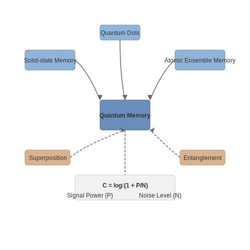
At its core, quantum memory is about storing quantum states for later retrieval. The functional principles are rooted in quantum superposition and entanglement. A single qubit can represent not just a 0 or 1, but both at once, a phenomenon known as superposition. When qubits are entangled, the state of one qubit can instantaneously affect the state of another, regardless of the distance between them. This non-local property is pivotal for advanced information technology applications, including quantum computing and secure quantum communication. The capacity to preserve these quantum states over time is essential for effective quantum computation. Research has demonstrated that certain materials, such as rare-earth-doped crystals and atomic ensembles, can be employed as quantum memories. These materials have the unique ability to minimize decoherence, an effect that leads to the degradation of quantum information due to interactions with the environment.Implementation of Quantum Memory
There are several methods to implement quantum memory, with notable approaches including:- Solid-state Quantum Memory: Utilizing materials like Yttrium Aluminum Garnet (YAG) doped with rare-earth ions, which can store qubits for extended periods due to their low decoherence rates.
- Atomic Ensemble-Based Memory: In this approach, an ensemble of atoms is used to map the information onto a collective state, leveraging techniques such as Electromagnetically Induced Transparency (EIT) to achieve long storage times.
- Quantum Dots: Semiconductor quantum dots serve as ideal qubit candidates due to their tunable energy levels and interactions with light.
Mathematical Description of Quantum Memory
To mathematically describe the efficiency and capacity of a quantum memory, one might consider the storage capacity \( C \) and fidelity \( F \):Applications of Quantum Memory
The application spectrum for quantum memory is truly expansive. Some key areas include:- Quantum Computing: Quantum memory forms the backbone of quantum processors, enabling the realization of complex algorithms and computations.
- Quantum Communication: With the advent of quantum key distribution (QKD), quantum memory allows for secure transmission of information, dramatically increasing communication security.
- Quantum Networks: The integration of quantum memories into networks allows for protocols that can outperform classical communications by enabling faster and more secure data exchange.
6.3 The Role of AI in Memory Technologies
As the landscape of memory technologies evolves, the integration of Artificial Intelligence (AI) stands out as a transformative influence. Enhancements in memory systems, driven by AI, signal a shift in how we process and utilize data. This subsection explores the synergy between AI and memory devices, focusing on advancements, methodologies, and practical applications.
Understanding AI's Impact on Memory Technology
The intersection of AI and memory technologies is primarily characterized by the latter's reliance on machine learning algorithms to optimize performance, manage data, and enhance operational efficiencies. AI enables memory systems to adaptively allocate resources, anticipating user demands. Through predictive analytics, memory systems can forecast usage patterns, thereby increasing reliability and speed in data access and retrieval.
Advanced Approaches to Memory Management
One notable approach involves the development of intelligent memory management systems. These systems make use of AI to improve memory allocation and avoid fragmentation, ensuring that memory resources are better utilized. For example, AI algorithms can analyze access patterns in real-time, adjusting the allocation dynamically.
Furthermore, with the rise of neuromorphic computing—a paradigm that draws inspiration from neural networks—AI plays a pivotal role in mimicking human cognition. This allows for more efficient memory structures that can learn and adapt. Here, the brain-inspired approach significantly reduces energy consumption while improving the speed of memory operations.
Real-World Applications and Case Studies
In industry applications, AI-assisted memory technologies have proven invaluable. For instance, in the realm of data centers, AI-driven algorithms manage workloads more effectively, optimizing data placement and retrieval to enhance performance. These developments lead to substantial cost savings in operation and energy consumption.
A practical example can be seen in the deployment of AI-driven SSDs, where algorithms prefetch likely accessed data into faster memory based on usage patterns. This leads to improved access times and overall system performance. Moreover, companies like Intel and Samsung are leveraging AI to improve the reliability of NAND flash memory technologies through predictive maintenance.
Challenges and Future Directions
Despite the promising synergy of AI with memory technologies, challenges such as data security and integrity must be addressed. AI systems can be vulnerable to attacks that exploit their learning algorithms. Therefore, future developments will likely focus on enhancing the robustness and security of AI-enhanced memory solutions.
Moreover, the need for efficient, scalable AI learning models is essential to accommodate the vast amounts of data generated by memory technologies. Innovations in quantum computing may also pave the way for new paradigms in memory devices, where AI algorithms will play a critical role in managing quantum states.
In conclusion, the role of AI in memory technologies not only enhances existing systems but also paves the way for groundbreaking innovations. As we advance, the integration of AI with memory technologies will be crucial in meeting the growing demands for speed, efficiency, and secure data handling.
7. Academic Journals
7.1 Academic Journals
As we delve into the study of applied memory devices, it becomes crucial to engage with the latest research and developments documented in academic journals. These publications serve as a cornerstone for understanding cutting-edge innovations and theoretical advancements in the field. Academic journals not only provide comprehensive research analyses but also present peer-reviewed information, which ensures the credibility and accuracy of the data presented.
Importance of Academic Journals in Memory Devices Research
Academic journals play a pivotal role in the dissemination of knowledge. They offer insights into:
- Emerging Technologies: Explore the latest innovations in memory storage technologies, such as non-volatile memory and quantum memory systems.
- Peer-Reviewed Research: Provides validation of scientific concepts and ensures that findings are scrutinized by experts before publication.
- Theoretical Developments: Addresses advancements in theoretical frameworks which underpin the practical applications of memory devices.
- Case Studies and Experiments: Discusses detailed experiments and case studies that highlight real-world applications and challenges.
Key Aspects of Research in Memory Devices
The field of applied memory devices includes several key elements:
- Material Science: Investigating materials like phase-change materials and ferroelectric polymers that offer new possibilities for memory device construction.
- Scaling and Miniaturization: Challenges related to shrinking device size while maintaining performance and reliability.
- Energy Efficiency: Developing memory solutions that consume less power without affecting speed or performance.
- Data Retention and Security: Ensuring that memory devices securely retain data over time without becoming vulnerable to breaches.
Renowned journals such as the Journal of Applied Physics and IEEE Transactions on Nanotechnology often present articles and papers focusing on these aspects.
Real-World Applications
Applied memory devices hold significance in various sectors, including:
- Consumer Electronics: From smartphones to laptops, memory devices play a crucial role in data storage and retrieval.
- Healthcare: Data from medical devices and patient records rely on advanced memory solutions for secure and efficient data storage.
- Automotive and Aviation: Memory systems in autonomous vehicles and aircraft require robust and reliable data storage solutions.
By understanding and engaging with academic literature, researchers and engineers can pave the way for future innovations in memory technology.
Further Reading
- IEEE Xplore Digital Library — A vast repository of electronics and engineering research papers, including extensive resources on memory devices and their applications.
- Journal of Applied Physics — Offers articles on the physics behind applied memory devices, highlighting both practical experiments and theoretical research.
- Journal of Memory and Language — Although primarily focused on cognitive sciences, it provides insights into memory as a concept applicable to device technology.
- Science and Engineering of Composite Materials — Explore the role of novel materials in advancing memory device technologies.
- Nature Nanotechnology — Covers research that includes nano-scale advancements in memory devices.
- Microelectronics Journal — Focuses on integrated circuits and memory solutions, especially as they apply to smaller scale and lower power devices.
- Journal of Nanotechnology in Engineering and Medicine — Discusses the intersections of nanotechnology and healthcare, with relevance to memory devices.
7.2 Books on Memory Technologies
- Memory Systems: Cache, DRAM, Disk — Explore a comprehensive overview of memory systems with an in-depth examination of memory architectures, algorithms, and techniques utilized in modern computing systems. Ideal for advanced learners interested in system-level memory design.
- Non-volatile Memory Database Management Systems — Discover the implications and applications of non-volatile memory in database management. This book provides insights into emerging database technologies and architectures that leverage persistent memory innovations.
- Memory Technologies — A thorough examination of both theoretical and practical aspects of memory technologies, focusing on the evolution of memory devices and their impact on data-intensive applications. Suitable for those researching next-gen memory solutions.
- Emerging Memory Technologies — Delve into new directions in memory technology including MRAM, FeRAM, and 3D memory, with discussions on design challenges and innovations. Perfect for researchers focusing on evolving trends in the memory industry.
- Cambridge Memory Technologies — Gain insights on contemporary memory technologies with illustrative case studies and real-world applications. This book is well-suited for professionals interested in the practical implementation of memory systems.
- Advanced Memory Technology — A detailed exploration into sophisticated memory technologies, including technical challenges and solutions in high-performance computing environments. An essential resource for engineers seeking cutting-edge knowledge in memory innovations.
- Resistive Switching: From Devices to Systems — Investigate the resistive switching phenomenon at the device and system level, exploring its potential in non-volatile memory applications. This book is tailored for those delving into resistive memory technologies.
7.3 Online Resources and Tutorials
In exploring applied memory devices, the wealth of online resources and tutorials available can significantly enhance your understanding and application of these advanced topics. As engineers, physicists, researchers, or graduate students, you can take advantage of several platforms that offer comprehensive theoretical knowledge, practical insights, and hands-on projects to better grasp the nuances of memory devices.
To facilitate your learning journey, here is a curated list of high-quality, topic-relevant online resources and tutorials:
- Electronics Tutorials — This website provides a wide range of tutorials on electronics, including memory device concepts, types, and applications.
- EDN Network — Offers in-depth articles and tutorials on ongoing advancements and practical implementations of electronic systems, including memory devices.
- Digi-Key Electronics — Featuring numerous resources and tutorials for understanding advanced memory components, product selection, and use cases in complex systems.
- All About Circuits Technical Articles — Provides technical articles that cater to detailed, research-backed information on memory technologies and their evolving trends.
- IEEE Xplore — A vast digital library of educational resources, conference papers, and journals to deepen your knowledge of electronic memory systems and their innovations.
- Coursera Electronics Courses — Offers specialized courses and video tutorials on various topics, including memory device architectures, types, and practical applications.
- edX Electrical Engineering — Provides comprehensive courses covering fundamental to advanced concepts in electronics, including memory device electronics.
- MIT OpenCourseWare YouTube — Access to free video lectures and courses from MIT, exploring topics such as solid state electronics and memory device technology.