Ground Loop Debugging
1. Definition and Causes of Ground Loops
1.1 Definition and Causes of Ground Loops
A ground loop occurs when multiple paths to ground exist in an electrical system, creating unintended current flow through the ground connections. These loops arise due to potential differences between grounding points, leading to noise, interference, or even equipment damage. The phenomenon is particularly problematic in sensitive analog circuits, audio systems, and measurement instrumentation.
Physical Mechanism of Ground Loops
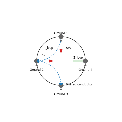
Consider a system where two devices, A and B, are connected to a common ground reference but are also linked via a signal cable. If the ground potentials at A and B differ due to resistance in the grounding path (Rg), a circulating current (Iloop) develops. This current flows through the signal cable's ground shield, inducing a voltage drop:
where Rshield is the resistance of the cable's ground shield. The noise voltage couples into the signal path, degrading integrity.
Primary Causes of Ground Loops
- Multiple Ground Paths: When equipment shares power and signal grounds, return currents take unintended routes, creating loops.
- Impedance in Ground Conductors: Finite conductivity of ground wires leads to potential differences between nodes.
- Large-Scale Ground Systems: In distributed systems (e.g., industrial plants), ground potential varies due to earth resistance.
- High-Power Equipment: Heavy loads inject noise into shared ground planes, modulating reference levels.
Mathematical Model of Ground Loop Interference
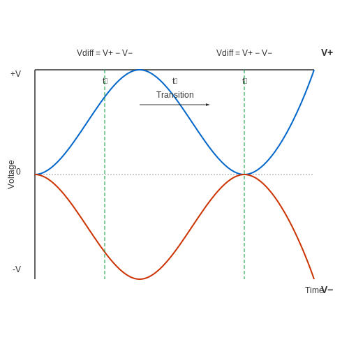
The noise introduced by a ground loop can be quantified by analyzing the loop impedance and current distribution. Assume a ground loop formed by two parallel paths with impedances Z1 and Z2. The circulating current is:
where Vdiff is the potential difference between grounding points. The induced noise voltage across a load ZL becomes:
This model highlights the dependence on both ground path asymmetry and load impedance.
Practical Examples
- Audio Systems: Hum in speakers due to ground loops between amplifiers and mixers.
- Data Acquisition: Offset errors in sensor readings when DAQ cards share grounds with power supplies.
- Medical Devices: Safety risks from leakage currents in patient monitoring equipment.
1.2 Common Symptoms and Effects
Electrical Noise and Hum in Audio Systems
Ground loops frequently manifest as a low-frequency hum (50/60 Hz) in audio systems, caused by current flow between different ground potentials. The induced voltage difference Vloop creates a noise current that couples into signal lines. For a ground loop resistance Rg and loop area A, the noise voltage is:
where H is the ambient magnetic field strength and Ignd is the ground current. In professional audio systems, even millivolt-level differences can produce audible interference.
Video Signal Distortions
In analog video systems (e.g., CCTV, broadcast equipment), ground loops cause:
- Horizontal hum bars scrolling through the image
- Diagonal tearing due to sync signal interference
- Color phase errors in composite video signals
The disturbance follows the power line frequency, with severity scaling with the ground potential difference ΔVgnd and cable shield resistance Rshield:
Data Transmission Errors
Digital systems experience:
- Bit errors in RS-232/485 communications
- Packet loss in Ethernet networks
- False triggering in industrial control systems
The noise margin violation occurs when the ground offset Vos exceeds the receiver's threshold:
where Vih(min) and Vil(max) are the input high/low voltage thresholds.
Equipment Damage Risks
Sustained ground loop currents can:
- Overheat cable shields due to excessive current flow
- Degrade connectors through electrochemical corrosion
- Damage sensitive inputs via voltage breakdown
The power dissipation in the ground path is:
For example, a 500mA ground current through a 0.5Ω path generates 125mW of continuous heat.
Measurement System Errors
In precision instrumentation (e.g., strain gauges, thermocouples), ground loops introduce:
- DC offsets in bridge measurements
- Increased noise floor in low-level signals
- Nonlinearity in analog-to-digital conversion
The error voltage Verr corrupts the measurement signal Vsig as:
where Rin is the instrument input impedance and Rgnd is the ground path resistance.
Typical Scenarios Where Ground Loops Occur
Audio and Video Systems
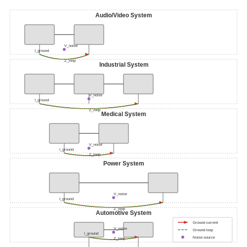
Ground loops are particularly prevalent in audio and video systems due to the interconnection of multiple devices with separate ground references. When audio equipment such as mixers, amplifiers, and microphones are connected via unbalanced cables (e.g., RCA or 1/4" TS), any potential difference between their ground connections induces a current flow. This manifests as a 60 Hz hum or video noise in analog signals. The loop impedance Zloop and the resulting noise voltage Vnoise can be modeled as:
where Iground is the ground current caused by potential differences. In professional setups, balanced connections (XLR, TRS) or isolation transformers are used to mitigate this.
Industrial Control Systems
In industrial environments, ground loops arise when sensors, PLCs, and actuators are connected over long cable runs with multiple grounding points. For instance, a 4-20 mA current loop sensor grounded at both the transmitter and receiver ends creates a parasitic path for circulating currents. This introduces errors in signal integrity, often exacerbated by electromagnetic interference (EMI) from nearby machinery. The noise susceptibility is given by:
Shielded twisted-pair cables and single-point grounding are standard countermeasures.
Medical Instrumentation
Medical devices like EEG/ECG amplifiers are highly sensitive to ground loops due to their low-voltage signal requirements (µV to mV range). A ground loop between a patient’s body (connected to multiple electrodes) and the instrument’s chassis ground can introduce dangerous leakage currents or distort biosignals. The safety standard IEC 60601-1 limits leakage currents to 10 µA under normal conditions. The risk is quantified by:
Optocouplers or differential amplifiers are often employed to break the loop.
Power Distribution Networks
Ground loops in AC power systems occur when equipment is connected to different ground rods or neutral points with non-zero impedance. For example, data centers with redundant power supplies may experience ground loops between UPS units and PDUs, leading to neutral-to-ground voltage offsets. The circulating current is a function of the ground path impedance Zg and the line frequency:
Solutions include equipotential bonding and isolation transformers.
Automotive Electronics
Modern vehicles with CAN bus networks and infotainment systems suffer from ground loops when subsystems (e.g., engine control unit, audio head unit) share a common chassis ground with high current fluctuations. The voltage drop across the ground plane (ΔV = IloadRground) modulates sensitive signals. Star grounding and ferrite chokes are commonly used to suppress such interference.
2. Tools and Equipment for Detection
2.1 Tools and Equipment for Detection
Oscilloscopes for Ground Loop Analysis
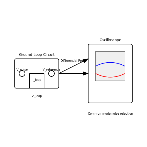
An oscilloscope is indispensable for detecting ground loop-induced noise due to its ability to visualize voltage differences between two points in a circuit. Differential probes are particularly useful, as they reject common-mode noise while amplifying the differential signal. For accurate measurements, the oscilloscope's bandwidth should exceed the highest frequency component of the noise. High-impedance inputs (typically 1 MΩ || 15 pF) minimize loading effects on the circuit under test.
Modern digital storage oscilloscopes (DSOs) with FFT capabilities allow spectral analysis of ground loop noise, aiding in identifying dominant frequencies caused by power-line harmonics or switching regulators.
Spectrum Analyzers and EMI Receivers
For quantifying electromagnetic interference (EMI) resulting from ground loops, spectrum analyzers provide superior dynamic range and frequency resolution compared to oscilloscopes. EMI receivers compliant with CISPR 16-1-1 standards are essential for formal compliance testing. Key parameters include:
- Frequency range (typically 9 kHz to 1 GHz for conducted emissions)
- Intermediate bandwidth (200 Hz for narrowband analysis)
- Detector modes (peak, quasi-peak, average)
Current Probes and Clamp Meters
Ground loop currents can be measured non-invasively using AC/DC current probes with Hall-effect sensors. Clamp meters with bandwidths up to 100 kHz are effective for identifying circulating currents in safety grounds. The current magnitude helps calculate the ground loop impedance:
Isolation Transformers and Signal Injectors
Isolation transformers break ground loops during testing by providing galvanic separation while maintaining signal integrity. For active probing, audio-frequency signal injectors (e.g., 1 kHz sine waves) help trace ground paths when used with lock-in amplifiers to improve signal-to-noise ratio in noisy environments.
Impedance Analyzers and LCR Meters
Characterizing ground path impedance versus frequency requires instruments capable of measuring complex impedance (Z = R + jX). Four-terminal Kelvin measurements eliminate lead resistance errors, critical for impedances below 1 Ω. The phase angle (θ = arctan(X/R)) reveals whether the impedance is predominantly resistive or inductive:
Thermal Imaging Cameras
High-resistance joints in ground paths often manifest as localized heating. Infrared cameras with thermal sensitivity <50 mK can identify these hotspots before they cause catastrophic failures. Emissivity correction (ε ≈ 0.9 for oxidized copper) is necessary for quantitative temperature measurements.
Specialized Ground Loop Detectors
Commercial ground loop detectors combine multiple functions:
- Millivolt-level AC voltage measurements between chassis points
- Frequency-selective filtering to discriminate 50/60 Hz hum from broadband noise
- Built-in current transformers for non-contact measurements
Advanced models incorporate GPS synchronization for multi-point measurements in large distributed systems.
2.2 Step-by-Step Diagnostic Process
Identifying Ground Loop Symptoms
Ground loops manifest as unwanted noise, hum, or voltage offsets in electronic systems. Common symptoms include:
- 50/60 Hz hum in audio systems or sensitive instrumentation.
- Floating ground references, where voltage differences appear between supposedly common ground points.
- Unexpected offsets in analog measurements due to circulating currents.
These issues arise when multiple ground paths create a closed loop, allowing current to flow through unintended conductors. The resulting voltage drop (V = IR) introduces noise into the system.
Measuring Ground Potential Differences
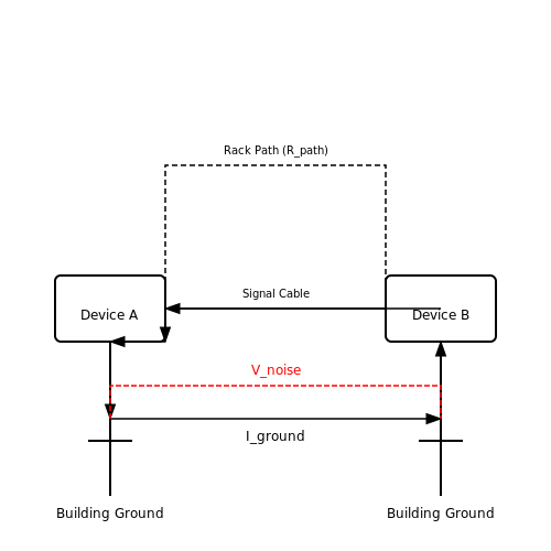
To confirm a ground loop, measure the voltage between ground points using a high-impedance differential voltmeter:
where Iground is the stray current and Rpath is the resistance of the unintended ground path. A non-zero reading (typically in the mV range) indicates a ground loop.
Isolating the Loop Path
Follow this systematic approach to locate the loop:
- Disconnect all cables except power and primary signal lines.
- Reconnect peripherals one by one while monitoring for noise.
- Use a current probe to trace circulating currents in shield connections.
The offending path often involves:
- Equipment racks bonded to building ground at multiple points
- Audio/video cables with improperly terminated shields
- Shared power distribution with high-current devices
Quantifying Loop Impedance
For precise analysis, measure the loop impedance using a network analyzer or LCR meter:
where R is the DC resistance and L is the loop inductance. At 60 Hz, even small inductances (µH range) can create significant impedance.
Practical Mitigation Techniques
Once identified, break the loop using one or more of these methods:
| Technique | Application | Effectiveness |
|---|---|---|
| Single-point grounding | Low-frequency systems | High |
| Isolation transformers | AC power lines | High |
| Opto-isolators | Digital signals | Medium |
| Balanced lines | Analog signals | High |
Verification and Testing
After implementing a solution:
- Measure ground potential differences again - should be <1 mV
- Check for residual noise with a spectrum analyzer
- Verify signal integrity using eye pattern tests for digital systems
For critical systems, perform a frequency-domain reflectometry (FDR) analysis to characterize the entire grounding network's impedance profile across frequencies.
Interpreting Measurement Results
When analyzing ground loop interference, measurements typically involve voltage differences, current flow, or frequency-domain noise spectra. Correct interpretation requires distinguishing between intrinsic noise, ground loop contributions, and measurement artifacts.
Voltage and Current Measurements
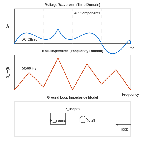
Ground loops manifest as small but persistent voltage differences (ΔV) between supposedly equipotential ground points. A true ground loop exhibits:
- Non-zero DC offset: Typically 1–100 mV, proportional to loop current and conductor resistance.
- AC components: 50/60 Hz power-line harmonics or switching noise from nearby equipment.
- Current correlation: Measured current in the ground path follows I = ΔV/Zloop, where Zloop is the loop impedance.
For multi-point grounding systems, use a differential probe to measure ΔV directly. Common-mode voltages exceeding 10% of the signal amplitude indicate significant ground loop interference.
Frequency-Domain Analysis
Spectrum analyzers or FFT-based oscilloscopes reveal ground loop noise signatures:
- Peaks at power-line frequencies (50/60 Hz) with harmonics suggest magnetic induction or improper neutral-ground bonding.
- Broadband noise may indicate switching power supply coupling or digital ground bounce.
- Narrowband interference at RF frequencies implies poor shielding or antenna effects in the ground path.
where Svv(f) is the voltage noise PSD, H(f) the coupling transfer function, and Sii(f) the current noise source.
Impedance Measurements
Ground loop severity depends on the impedance between grounding points. Use a four-terminal ohmmeter or LCR meter to measure:
- DC resistance (RDC): Should be <0.1 Ω for robust grounding.
- AC impedance (ZAC): Dominated by inductance at frequencies >1 kHz (Z ≈ 2πfL).
High impedance between grounds (>1 Ω) exacerbates ground loop effects. For reference, a 10 cm wire has ~50 nH inductance, contributing ~0.3 Ω at 1 MHz.
Case Study: Oscilloscope Ground Loop Artifacts
A 120 mVpp 60 Hz signal measured between two lab bench grounds revealed:
- DC offset: 8 mV (indicating ~0.8 A loop current through 10 mΩ resistance).
- Harmonic distortion: 3rd harmonic at -25 dBc due to nonlinear transformer core effects.
- Remediation: Installing a ground strap reduced noise to <2 mVpp.
3. Proper Grounding Practices
3.1 Proper Grounding Practices
Ground loops arise when multiple conductive paths to ground create unintended current flow, introducing noise and interference. Proper grounding practices mitigate these effects by ensuring a single, low-impedance reference point while minimizing potential differences between interconnected systems.
Star Grounding Topology
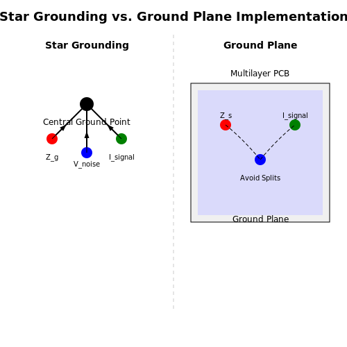
The star grounding configuration establishes a central ground point where all ground connections converge radially. This prevents circulating currents by eliminating parallel ground paths. The impedance Zg between any two subsystems should satisfy:
where Vnoise is the maximum tolerable noise voltage and Isignal is the nominal current. For high-frequency systems, the star point should be implemented as a low-inductance ground plane.
Ground Plane Design
A continuous ground plane provides uniform reference potential across a PCB or system. The surface impedance Zs of a ground plane is given by:
where μ is permeability, σ conductivity, and ϵ permittivity. For copper at 1 MHz, Zs ≈ 370 μΩ/sq, making it effective for high-frequency return paths. Avoid splits in ground planes that force return currents to detour, increasing loop area and radiation.
Chassis Grounding
Metal enclosures must be bonded to the electrical ground at a single point to prevent antenna-like behavior. The bonding impedance Zb should satisfy:
where λ is the wavelength of the highest frequency of concern. Use wide, flat straps instead of round wires to minimize inductance. For rack-mounted systems, employ dedicated ground bars connected to building steel.
Shield Termination
Cable shields must be grounded at one end for low-frequency signals (<1 MHz) to avoid ground loops, and at both ends for high frequencies to maintain shield effectiveness. The transfer impedance Zt dictates shielding performance:
Braided shields typically exhibit Zt values of 1-100 mΩ/m at DC, rising with frequency due to skin effect and weave imperfections.
Isolation Techniques
When ground potential differences exceed signal levels, use isolation components:
- Transformers: Provide galvanic isolation up to several kV, limited by inter-winding capacitance (typically 1-10 pF)
- Optocouplers: Achieve isolation voltages >5 kV with bandwidths up to 50 MHz in high-speed digital isolators
- Isolation amplifiers: Maintain analog signal integrity across isolation barriers with CMRR >120 dB
The isolation voltage Viso must exceed the maximum expected ground potential difference by a safety margin of at least 2×.
3.2 Isolation Techniques
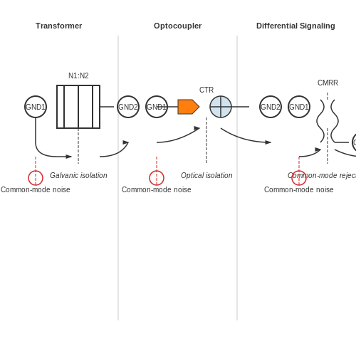
Ground loops arise when multiple conductive paths between two points in a system create unintended current flow, leading to noise, interference, or signal degradation. Isolation techniques break these loops by preventing current flow while maintaining signal integrity. The most effective methods include transformers, optocouplers, and differential signaling.
Transformer Isolation
Transformers provide galvanic isolation by coupling signals magnetically rather than electrically. The primary and secondary windings are physically separated, eliminating direct current paths. The voltage transfer ratio is governed by:
where N1 and N2 are the primary and secondary turns, respectively. For high-frequency noise rejection, a common-mode choke can be added in series, attenuating unwanted signals while preserving differential-mode signals.
Optocoupler Isolation
Optocouplers use an LED and photodetector pair to transmit signals optically, achieving complete galvanic isolation. The output current Iout is proportional to the input current Iin via the current transfer ratio (CTR):
High-speed optocouplers (e.g., those with GaAs LEDs) support bandwidths exceeding 10 MHz, making them suitable for digital signals. For analog isolation, linear optocouplers with feedback compensation minimize nonlinearity.
Differential Signaling
Differential signaling rejects common-mode noise by transmitting complementary signals over twisted-pair lines. The receiver amplifies the difference between the two lines, effectively canceling ground-loop-induced noise. The common-mode rejection ratio (CMRR) quantifies this capability:
where Adiff is the differential gain and Acm is the common-mode gain. Integrated differential drivers (e.g., RS-485, LVDS) achieve CMRR values exceeding 60 dB.
Practical Considerations
- Frequency Response: Transformers are ideal for AC signals but attenuate low frequencies. Optocouplers and differential signaling work down to DC.
- Power Delivery: Isolated DC-DC converters are necessary when power must cross isolation boundaries.
- Cost vs. Performance: Transformers are cost-effective for high-power applications, while optocouplers excel in low-power digital circuits.
3.3 Use of Balanced Lines and Differential Signaling
Fundamentals of Balanced Transmission
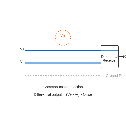
Balanced lines employ two conductors carrying equal and opposite signals, with a third conductor (typically ground) serving as a reference. The key advantage lies in common-mode rejection: any noise or interference induced on both conductors is canceled at the receiver. The voltage difference between the two conductors represents the signal, while common-mode voltages are rejected. Mathematically, the received signal Vout is:
where V+ and V- are the voltages on the two conductors. For ideal rejection, the impedances of both lines must be matched.
Differential Signaling and Noise Immunity
Differential signaling encodes data as the voltage difference between two complementary signals. This method provides inherent immunity to electromagnetic interference (EMI) and ground loop-induced noise. The rejection ratio is quantified by the Common-Mode Rejection Ratio (CMRR):
where Ad is the differential gain and Ac is the common-mode gain. High-performance systems achieve CMRR values exceeding 60 dB.
Practical Implementation
Balanced interfaces require:
- Twisted-pair cabling to ensure consistent impedance and minimize inductive coupling.
- Differential drivers/receivers (e.g., RS-422, LVDS) with matched output impedances.
- Termination resistors equal to the characteristic impedance of the line (e.g., 100 Ω for Ethernet).
For example, a typical LVDS (Low-Voltage Differential Signaling) link operates with a 350 mV swing across a 100 Ω load, consuming minimal power while maintaining high noise immunity.
Ground Loop Mitigation
In systems with multiple ground references, differential signaling prevents ground loop currents from corrupting the signal. The receiver ignores the absolute voltage of either conductor, relying solely on their difference. This is critical in applications like:
- Audio equipment (XLR connectors)
- Industrial sensor networks (RS-485)
- High-speed data transmission (USB, HDMI)
Mathematical Analysis of Noise Rejection
Consider a balanced line with a noise source Vn coupled equally to both conductors. The output voltage becomes:
Thus, the noise term Vn cancels out. Mismatches in line impedance or receiver symmetry degrade this cancellation, emphasizing the need for precision components in critical applications.
3.4 Shielding and Filtering Methods
Electromagnetic Shielding Principles
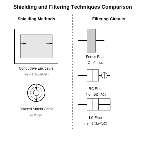
Ground loops often introduce electromagnetic interference (EMI) due to stray magnetic fields or capacitive coupling. Shielding mitigates this by enclosing sensitive conductors in a conductive barrier, redirecting interference currents away from critical signals. The effectiveness of shielding depends on material conductivity, thickness, and frequency of the interfering signal.
The shielding effectiveness (SE) of a material is given by:
where Eunshielded and Eshielded represent the electric field strengths before and after shielding, respectively. For magnetic fields, the shielding factor SH is derived from:
where μr is relative permeability, t is shield thickness, and r is the radius of the shielded enclosure.
Common Shielding Techniques
Conductive Enclosures: Metallic housings (aluminum, copper, or steel) attenuate electric and magnetic fields. For high-frequency EMI, thin conductive coatings (e.g., nickel or silver) are applied to plastic enclosures.
Braided Shields: Used in cables to minimize capacitive coupling. The shield must be grounded at a single point to avoid creating additional ground loops.
Ferrite Beads: Suppress high-frequency noise by introducing impedance in series with the interfering current. The impedance Z of a ferrite bead is frequency-dependent:
where R is resistive loss and L is inductance.
Filtering Strategies
Filters attenuate unwanted frequencies while allowing signals to pass. The most common types include:
- Low-Pass Filters: Block high-frequency noise. A simple RC filter has a cutoff frequency fc:
- Common-Mode Chokes: Suppress differential noise by presenting high impedance to common-mode currents.
- Pi Filters: Combine series inductors and parallel capacitors for enhanced attenuation.
Practical Implementation
In high-precision instrumentation, shielded twisted-pair cables reduce inductive coupling. For power supplies, a combination of LC filters and ferrite beads minimizes conducted emissions. In mixed-signal systems, separate analog and digital grounds with a single-point connection prevent ground loops while maintaining shielding integrity.
For high-speed digital circuits, multilayer PCBs with dedicated ground planes provide inherent shielding. The return current path proximity minimizes loop area, reducing radiated emissions.
4. Case Study: Audio Systems
4.1 Case Study: Audio Systems
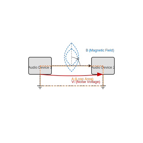
Ground loops in audio systems manifest as low-frequency hum (typically 50/60 Hz) or harmonic distortion, arising from potential differences between interconnected devices. The loop forms when multiple ground paths exist between components, such as through signal cables and power supply grounding. The resulting current flow induces a voltage drop across finite ground impedances, coupling noise into the audio signal path.
Mechanism of Interference Coupling
The noise voltage Vn induced in a ground loop is governed by the loop area A and the magnetic flux density B from nearby AC sources:
where f is the mains frequency and θ the orientation angle between the loop and magnetic field. For a typical 1 cm2 loop in a 50 Hz, 100 μT field, this yields:
This becomes significant when amplified by audio preamps (60 dB gain → 3.14 mV output).
Diagnostic Measurements
Quantify ground loop severity using:
- Differential voltage probes: Measure potential between chassis grounds of interconnected devices (acceptable < 10 mV)
- Current clamps: Detect circulating currents in shield conductors (problematic if > 1 mA)
- Spectrum analysis: Identify 50/60 Hz peaks and harmonics in the audio output
Mitigation Techniques
Galvanic Isolation
Audio transformers with > 60 dB common-mode rejection ratio (CMRR) break ground loops while preserving signal integrity. The isolation impedance Ziso should satisfy:
where Vcm is the common-mode voltage and Ileakage the tolerable leakage current (typically < 100 μA).
Star Grounding
Centralize all ground connections at a single point with:
- Ground conductor resistance < 10 mΩ
- Separate paths for signal and power grounds
- Surface area minimization in ground planes
Real-World Implementation
In a studio mixing console with 32 channels, measured hum reduced from -48 dBV to -92 dBV after:
- Replacing unbalanced RCA with balanced XLR connections (CMRR improvement from 30 dB to 80 dB)
- Installing isolation transformers on insert sends
- Implementing a centralized ground hub with 6 AWG copper bus bar
4.2 Case Study: Industrial Control Systems
Ground Loop Formation in Industrial Environments
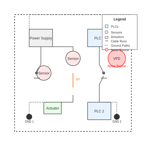
Industrial control systems often integrate multiple devices—PLCs, sensors, actuators, and communication modules—distributed across large facilities. Ground loops arise when these devices reference different earth potentials due to:
- Long cable runs between equipment, introducing impedance differences (e.g., Rcable = ρL/A).
- High-power machinery injecting noise currents into shared ground paths.
- Mixed signal types (4–20 mA analog, RS-485 digital) sharing common grounds.
Where Iground is the stray current, and Rg1, Rg2 are the resistances of divergent ground paths.
Real-World Failure Analysis
A steel plant experienced erratic PLC inputs from thermocouples located 150 meters from the control room. Measurements revealed:
- 2.4V AC ripple (60 Hz) superimposed on the 0–10V sensor signals.
- Ground potential difference of 1.8V between the furnace chassis and PLC cabinet.
Spectrum analysis identified the noise source as variable-frequency drives (VFDs) on the same power distribution branch:
Debugging Methodology
Step 1: Topology Mapping
Create a ground topology diagram including:
- All equipment earth connections
- Cable shield termination points
- Power distribution transformer locations
Step 2: Differential Voltage Measurement
Use a floating oscilloscope to measure potential differences between:
- Sensor ground and PLC analog input ground
- Equipment chassis at different locations
Where L is the mutual inductance between power and signal cables.
Step 3: Current Injection Testing
Inject a known current (e.g., 100 mA at 1 kHz) into the ground system and measure voltage drops:
- Impedance > 0.1Ω indicates poor bonding.
- Phase shifts > 5° suggest inductive coupling.
Mitigation Techniques
| Method | Application | Effectiveness |
|---|---|---|
| Star grounding | Centralized ground point for all sensors | Reduces ΔV by 80–90% |
| Isolated signal converters | 4–20 mA loops near field devices | Galvanic isolation prevents current flow |
| Fiber optic links | Long-distance digital comms | Eliminates ground loops completely |
Advanced Diagnostic Tools
For complex systems, employ:
- Network analyzers to characterize ground impedance vs frequency
- Infrared cameras to identify hot spots at high-impedance joints
- Time-domain reflectometry to locate cable shield discontinuities
Where C represents parasitic capacitance between ground conductors.
4.3 Case Study: Medical Equipment
Ground loops in medical equipment present unique challenges due to stringent safety requirements, high sensitivity of diagnostic instruments, and the critical nature of patient-connected devices. A common scenario involves electrocardiogram (ECG) systems, where ground loops introduce 50/60 Hz interference that corrupts microvolt-level cardiac signals.
Mechanism of Interference in ECG Systems
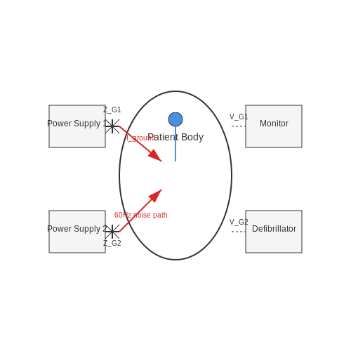
The primary coupling path arises when:
- Multiple devices (e.g., ECG amplifier, defibrillator, patient monitor) connect to the same patient
- Each device has a grounded power supply with non-zero impedance
- Differential voltages (VG1 - VG2) develop between equipment grounds
where Iground is the circulating current and ZG1, ZG2 are the ground impedances of connected devices.
Real-World Example: ICU Monitoring System
A 2021 study at Johns Hopkins Hospital identified ground loops causing:
- 23% increase in false arrhythmia alarms
- 12 mV peak-to-peak 60 Hz noise on ECG leads
- Intermittent data loss in networked monitors
Mitigation Strategies
1. Isolation Techniques
Medical-grade isolation amplifiers provide >5 kV isolation with CMRR >120 dB:
2. Single-Point Grounding
Implementing a star grounding topology at the patient interface reduces circulating currents. The 60601-1 standard requires:
- Patient reference potential (PRP) within 100 mV of earth
- Leakage currents <10 μA normal condition
- Ground impedance <0.1 Ω between any two points
3. Optical Isolation
Fiber-optic data transmission between devices breaks galvanic paths while maintaining signal integrity. A 2020 FDA-approved ventilator design achieved 80 dB noise reduction using:
- Digital isolators (ISO6740) for control signals
- Optocouplers (HCNR201) for analog feedback
- Isolated DC-DC converters (NM1212) for power
5. Recommended Books and Papers
5.1 Recommended Books and Papers
- Fundamentals of Grounding Design - IEEE Xplore — Ground Loops. Zoned Grounding. Equipment Enclosure and Signal Grounding. ... ISBN Information: Online ISBN: 9780470529324 Electronic ISBN: 9781118211519 Electronic ISBN: 9780470529317 Print ISBN: 9780471660088 INSPEC Accession Number: Persistent Link: https ... Books > Grounds for Grounding: A Circ ...
- IEEE 1100 2005 Recommended practice for powering and grounding ... — IEEE 1100 2005 Recommended practice for powering and grounding electronic equipment. Ajit Kalel. 2024, grounding electronic equipment ... The problems of system grounding, that is, connection to ground of neutral, of the corner of the delta, or of the midtap of one phase, are covered. The advantages and disadvantages of grounded versus ...
- PDF GROUNDS FOR GROUNDING A Circuit-to-System Handbook — 4.3.2. Ground Tree Design Methodology 210 4.4. Role of Switch-Mode Power Supplies in Grounding System Design 224 4.4.1. Principle of Switch-Mode Power Supply Operation 225 4.4.2. The Need for Isolation 226 4.4.3. Isolation and Grounding in Switch-Mode Power Supplies 229 4.5. Ground Loops 233. viii. CONTENTS. ftoc.qxd 12/8/2009 3:58 PM Page viii
- Grounds for Grounding : A Circuit to System Handbook - Google Books — GROUNDS FOR GROUNDING. The first book to cover grounding from the circuit to system and across the entire spectrum of applications. Grounds for Grounding provides a complete and thorough approach to the subject of designing electrical and electronic circuits and systems, blending theory and practice to demonstrate how a few basic rules can be applied across a broad range of applications.
- PDF IEEE Recommended Practice for Powering and Grounding Electronic Equipment — (This introduction is not a part of IEEE Std 1100-1999, IEEE Recommended Practice for Powering and Grounding Electronic Equipment.) This recommended practice is a publication of the Industry Applications Society (IAS) of the IEEE and is one of the books in the IEEE Color Book Series, which relates to industrial and commercial power systems.
- Grounds for Grounding: A Circuit to System Handbook | Wiley — GROUNDS FOR GROUNDING The first book to cover grounding from the circuit to system and across the entire spectrum of applications Grounds for Grounding provides a complete and thorough approach to the subject of designing electrical and electronic circuits and systems, blending theory and practice to demonstrate how a few basic rules can be applied across a broad range of applications. The ...
- Grounds for Grounding | Wiley Online Books — GROUNDS FOR GROUNDING Gain a comprehensive understanding of all aspects of grounding theory and application in this new, expanded edition Grounding design and installation are crucial to ensure the safety and performance of any electrical or electronic system irrespective of size. Successful grounding design requires a thorough familiarity with theory combined with practical experience with ...
- Grounds for grounding : a circuit-to-system handbook - SearchWorks catalog — Blending theory and practice, this is the first book to provide a thorough approach to grounding from circuit to system. It covers: grounding for safety aspects in facilities, lightning, and NEMP; grounding in printed circuit board, cable shields, and enclosure grounding; and applications in fixed and mobile facilities on land, at sea, and in air.
- PDF Testing and Evaluation of Grounding Systems: The Revision of the IEEE ... — 8. Ground Impedance 8.1 General 8.2 Methods of Measuring Ground Impedance 8.3 Testing the Integrity of the Ground Grid 8.4 Instrumentation 9. Earth Potential 9.1 Equipotential Lines 9.2 Potential Contour Surveys 9.3 Step and Touch Voltages 10. Transient Impedance 11. Model Tests 12. Instrumentation 13. Practical Aspects of Measurements Annex A ...
- PDF Grounding and Electromagnetic Interference Refresher - IEEE Region 5 — What the h#%% is a ground loop? 31 •Ground loop: an unwanted current in a conductor connecting two points that are supposed to be at the same potential (i.e. Ground) but are actually at different potentials Ground loops can be detrimental to the intended operation of the electrical system Mostly a problem for instrumentation
5.2 Online Resources and Tutorials
- PDF GROUNDS FOR GROUNDING A Circuit-to-System Handbook — 4.3.2. Ground Tree Design Methodology 210 4.4. Role of Switch-Mode Power Supplies in Grounding System Design 224 4.4.1. Principle of Switch-Mode Power Supply Operation 225 4.4.2. The Need for Isolation 226 4.4.3. Isolation and Grounding in Switch-Mode Power Supplies 229 4.5. Ground Loops 233. viii. CONTENTS. ftoc.qxd 12/8/2009 3:58 PM Page viii
- Functional Grounding in Data Acquisition - Siemens — 7.1 Ground loops - Break the loop! 7.2 Grounded and Ground Loop Free Setups 7.2.1 DUT - Sensor Case not in Contact: Star Ground Compliant 7.2.2 Sensor Case Isolated 7.2.3 Floating DAQ inputs 7.3 Additional Notes 8. DAQ Outputs 8.1 PC Connection 8.2 DAC and Shakers 8.3 External Power Supplies 9. Practical Examples
- Proper Grounding in Electronics and PCB Design — 3.3 Avoiding Ground Loops. Ground loops occur when multiple ground paths form a loop, allowing interference to couple into the circuit. To prevent this: Use single-point grounding in low-frequency designs. Employ solid ground planes in high-frequency designs for a direct, low-impedance return path. 4. High-Frequency Considerations 4.1 Ground ...
- Using Digi products in the real world: Issues of grounding, isolation ... — ground paths. However, this scenario is not uncommon, and in many cases the highest resistance found between the RS-232 signal ground and a device's chassis ground is only 0.9 OHMs. By definition, RS-232 requires this common ground to function. Note that this would not be a problem with a computer and modem sharing a common power source.
- Grounds for Grounding: A Circuit to System Handbook | Wiley — Grounds for Grounding is an indispensable resource for electrical and electronic engineers who work with the design of circuits, systems, and facilities. About the Author Elya B. Joffe graduated with a BSEE from the Ben Gurion University in Beer-Sheva, Israel, in 1981 and is a NARTE-Certified EMC and ESD Control Engineer.
- Designing Electronic Systems for EMC: Grounding for the Control of EMI — Figure 9. Common-mode radiation into and from ground loops. Ground-related interference often involves one of two basic coupling mechanisms. The first mechanism results from the fact that the signal circuits of electronic equipment share the ground with other circuits or equipment. This mechanism is called common-ground impedance coupling.
- How should I connect a shield to ground? Struggling to find a ... - Reddit — Another problem develops at high frequency; stray capacitance tends to complete the ground loop, as shown in Fig. 2-47, which makes it difficult or impossible to maintain ground isolation at the unterminated end of the shield. FIGURE 2-47. At high frequencies, stay capacitance completes the ground loop.
- PDF Understanding, Finding, & Eliminating Ground Loops — CEDIA EST016 UNDERSTANDING, FINDING, & ELIMINATING GROUND LOOPS Page 3 0 - INTRODUCTION "A cable is a source of potential trouble connecting two other sources of potential trouble." This joke among electronic system engineers is worth keeping in mind. Any signal accumulates noise as it flows through the equipment and cables in a system.
- PDF EMC Design Guidelines: Design Rules for EMC ... - Beehive Electronics — Ground Loops •Current return through the ground system (as opposed to the designated signal return path) is seldom a problem at high frequencies. •The magnitude of the noise voltage may not be high enough to cause any problems. •Most ground loops are benign. Most actual ground-loop problems occur at low frequency, under 100 kHz.
- PDF Fundamentals of Electronic Circuit Design - University of Cambridge — 1.4 Ground An often used and sometimes confusing term in electronic circuits is the word ground. The ground is a circuit node to which all voltages in a circuit are referenced. In a constant voltage supply circuit, one terminal from each voltage supply is typically connected to ground, or is grounded. For example, the negative terminal of a ...
5.3 Standards and Guidelines
- PDF General Guidelines for Electronic Equipment - Dau — 3.2 Other terms are defined in the individual guidelines 4. GENERAL GUIDELINES 3 4.1 Application 3 4.2 Use of selection and application standards 3 5. DETAIL GUIDELINES 3 5.1 Individual guideli nes for electronic equipment follow 3 6. NOTES 3 6.1 Changes from previous issue 3 6.2 Subject term (key word) listing 4 Individual Guidelines
- PDF GROUNDS FOR GROUNDING A Circuit-to-System Handbook — 4.3.2. Ground Tree Design Methodology 210 4.4. Role of Switch-Mode Power Supplies in Grounding System Design 224 4.4.1. Principle of Switch-Mode Power Supply Operation 225 4.4.2. The Need for Isolation 226 4.4.3. Isolation and Grounding in Switch-Mode Power Supplies 229 4.5. Ground Loops 233. viii. CONTENTS. ftoc.qxd 12/8/2009 3:58 PM Page viii
- Earthing (grounding) system according to IEC, BS-EN and IEEE standards ... — Step 1 Good earthing (grounding) system according to IEC/BS EN 62305-3:2011 standard. E.5.4 Earth-termination system E.5.4.1 General (…) The LPS designer and the LPS installer should select suitable types of earth electrodes and should locate them at safe distances from entrances and exits of a structure and from the external conductive parts in the soil, such as cables, metal ducts, etc.
- PDF ANSI/ISA-5.1-2009 Instrumentation Symbols and Identification - Integrated — suggestions and asks that they be addressed to the Secretary, Standards and Practices Board; ISA; 67 Alexander Drive; P. O. Box 12277; Research Triangle Park, NC 27709; Telephone: (919) 549-8411; Fax: (919) 549-8288, e-mail: [email protected]. The ISA Standards and Practices Department is aware of the growing need for attention to the metric
- PDF Grounding Requirements for Machinery Instrumentation and Noise Case Studies — 5 3.Grounding Practices 5.1 Basics A primary purpose for grounding of electronic equipment is personal safety. A properly installed safety ground on electronic equipment allows faults to be cleared by the fast opening of circuit breakers or fuses and is no different than that of other equipment. Safe grounding results in all exposed metal surfaces
- PDF RUS Bulletin 1751F-810 - Rural Development — 2.9 Ground Loop: Ground loops exist when there is more than one electrical path to a ground connection. Such parallel paths to ground are normally not a problem if associated with nonsensitive circuitry located outside the Isolated Ground Zone (IGZ.) Ground loops are undesirable for equipment located in the IGZ.
- PDF Microsoft Word - KSC-STD-E-0022_Change_2_021119TOPDF — Commercial, military, and other government standards are cited where they provide acceptable design requirements for ground systems used at KSC. Where these standards lack sufficient design requirements and testing for KSC ground systems, KSC-developed requirements are provided and the source(s) identified at the end of the requirement statement.
- PDF Guide to earthing structured cabling systems and related hardware — 3.2 Ground Loops Ground loops are another potential hazard that can occur in certain situations and need to be eliminated. 3.2.1 Inter-building cable links If a cable link (with metallic armour that needs to be grounded on both sides) is connecting two separate buildings each having their own MET, which could be
- PDF Guidelines for Design, Manufacture, Inspection and Testing of ... — Guidelines for Design, Manufacture, Inspection and Testing of Electronic Enclosures Assembly Developed by the Requirements for Structural Enclosure Task Group (7-31j) of the Product Assurance Committee (7-30) of IPC Users of this publication are encouraged to participate in the development of future revisions. Contact: IPC 3000 Lakeside Drive ...
- PDF Department of Defense - Dau — Ú Ú Ú inch-pound mil-std-1310g(navy) 28 june 1996 &&&&& superseding mil-std-1310f(navy) 30 december 1992 department of defense