Noise Reduction Techniques in Circuits
1. Types of Noise in Circuits
Types of Noise in Circuits
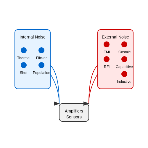
Thermal Noise (Johnson-Nyquist Noise)
Thermal noise arises due to the random motion of charge carriers in a conductor at finite temperature. It is present in all resistive elements and is independent of the applied voltage or current. The power spectral density (PSD) of thermal noise is given by:
where k is Boltzmann's constant (1.38 × 10⁻²³ J/K), T is absolute temperature in Kelvin, and R is resistance. The RMS noise voltage across a bandwidth B is:
This white noise spectrum remains flat up to extremely high frequencies (~1013 Hz at room temperature). In practice, thermal noise limits the sensitivity of precision measurement systems such as medical instrumentation and radio astronomy receivers.
Shot Noise
Shot noise occurs due to the discrete nature of charge carriers in devices where current flows across potential barriers (diodes, transistors). The noise current spectral density is:
where q is electron charge (1.6 × 10⁻¹⁹ C) and IDC is average current. Unlike thermal noise, shot noise depends on bias current and follows Poisson statistics. It becomes significant in:
- Photodetectors and avalanche diodes
- Low-current semiconductor junctions
- High-speed digital circuits with fast switching edges
Flicker Noise (1/f Noise)
Flicker noise exhibits a spectral density inversely proportional to frequency:
where K is a device-specific constant and α typically ranges from 0.8 to 1.2. This noise dominates at low frequencies (below 1 kHz) and originates from:
- Trapping/detrapping of carriers at material defects (MOSFETs)
- Surface recombination in bipolar transistors
- Contact resistance fluctuations
In analog IC design, flicker noise critically impacts the performance of operational amplifiers and mixers in the audio frequency range.
Burst Noise (Popcorn Noise)
A non-Gaussian noise characterized by discrete switching between two or more voltage levels, typically with time constants in the millisecond range. The power spectrum follows Lorentzian distribution:
Burst noise originates from heavy metal ion contamination in semiconductors or defects in crystal lattice. It is particularly problematic in:
- Precision voltage references
- Low-noise oscillators
- Biomedical signal acquisition circuits
Avalanche Noise
Occurs in reverse-biased p-n junctions near breakdown voltage, where carrier multiplication creates random current pulses. The noise power increases exponentially with reverse bias:
where VR is reverse voltage and VB is breakdown voltage. This noise mechanism is exploited intentionally in avalanche photodiodes for single-photon detection but must be minimized in voltage regulators.
Quantization Noise
Introduced by analog-to-digital conversion when mapping continuous signals to discrete levels. For an N-bit ADC with step size Δ, the noise power is:
This white noise spectrum spreads uniformly up to the Nyquist frequency. Oversampling techniques can reshape this noise through sigma-delta modulation, pushing most of the noise power beyond the band of interest.
1.2 Sources of Noise in Electronic Systems
Thermal Noise (Johnson-Nyquist Noise)
Thermal noise arises from the random thermal motion of charge carriers in a conductor. It is present in all resistive elements and is frequency-independent (white noise) up to extremely high frequencies. The noise voltage spectral density Sv(f) is given by:
where k is Boltzmann's constant (1.38 × 10⁻²³ J/K), T is absolute temperature, and R is resistance. The total RMS noise voltage across bandwidth B is:
In practice, thermal noise limits the sensitivity of high-impedance circuits such as preamplifiers and RF receivers.
Shot Noise
Shot noise occurs due to the discrete nature of charge carriers in devices with potential barriers (diodes, transistors). It follows Poisson statistics and has a current spectral density:
where q is electron charge (1.6 × 10⁻¹⁹ C) and IDC is the average current. Unlike thermal noise, shot noise depends on current flow rather than temperature.
Flicker Noise (1/f Noise)
Flicker noise dominates at low frequencies (< 1 kHz) in semiconductors and thin-film resistors. Its power spectral density follows:
where K is a device-specific constant and α typically ranges from 0.8 to 1.3. The physical origins include trap states in MOSFET gate oxides and contact imperfections in resistors.
Popcorn Noise (Burst Noise)
Popcorn noise appears as discrete step changes in current/voltage due to meta-stable defects in semiconductors. Its power spectrum shows Lorentzian peaks:
where fc is the corner frequency (typically 1-100 Hz). This noise is prominent in poorly fabricated bipolar transistors and some CMOS processes.
Quantization Noise
In digital systems, quantization noise arises from the finite resolution of analog-to-digital conversion. For an N-bit ADC with full-scale range VFSR, the noise power is:
This noise appears as a uniform distribution across the Nyquist bandwidth and sets the theoretical signal-to-noise ratio (SNR) limit.
Environmental Noise Sources
- Power supply noise: Ripple and switching artifacts from regulators
- Ground loops: Current-induced voltage differences in shared return paths
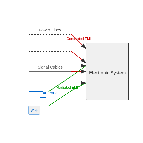
- Electromagnetic interference (EMI): Radiated coupling from nearby transmitters or digital circuits
- Microphonics: Mechanical vibration modulating component parameters
Noise Coupling Mechanisms
Noise propagates through circuits via:
- Conductive coupling: Direct connection through wires or PCB traces
- Capacitive coupling: Electric field interaction between adjacent conductors
- Inductive coupling: Magnetic field linkage between current loops
- Radiative coupling: Far-field electromagnetic wave reception
1.3 Impact of Noise on Circuit Performance
Signal-to-Noise Ratio (SNR) Degradation
Noise directly reduces the effective signal-to-noise ratio (SNR) in a circuit, limiting its ability to distinguish meaningful signals from background interference. The SNR is defined as:
where Psignal and Pnoise are the power levels of the signal and noise, respectively. In high-gain amplifiers or sensitive analog front-ends, even microvolt-level noise can corrupt weak signals, reducing SNR to unusable levels.
Nonlinear Distortion and Intermodulation
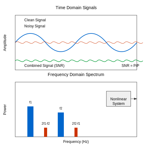
Noise interacting with nonlinear circuit elements (e.g., transistors, diodes) generates intermodulation products. For a nonlinear system described by a Taylor expansion:
noise components at frequencies f1 and f2 produce spurious outputs at f1 ± f2, 2f1 - f2, etc. This is particularly problematic in RF systems where spectral purity is critical.
Phase Noise in Oscillators
In timing circuits, noise causes phase noise, characterized by the Lorentzian spectrum:
where Q is the resonator quality factor, f0 is the carrier frequency, and FOM is the oscillator figure of merit. Phase noise degrades clock jitter and communication system bit-error rates (BER).
Noise in Digital Systems
While digital circuits are less susceptible to amplitude noise, timing jitter from clock noise affects setup/hold margins. The rms jitter (σt) relates to phase noise spectral density Sφ(f) via:
This becomes critical in high-speed serial links (e.g., PCIe, DDR) where picosecond-level jitter causes eye diagram closure.
Noise-Induced Bias Errors
In precision analog circuits (e.g., instrumentation amplifiers, ADCs), low-frequency 1/f noise introduces DC offsets. The noise power spectral density follows:
where K is a process-dependent constant. This necessitates chopper stabilization or auto-zeroing techniques in nanovolt-sensitive applications.
Case Study: Noise in LNA Design
A 2.4 GHz low-noise amplifier (LNA) with NF = 1.5 dB and G = 20 dB sees its output noise floor elevated by:
This sets the minimum detectable signal level for the entire receiver chain.
2. Shielding and Grounding Strategies
2.1 Shielding and Grounding Strategies
Electromagnetic Shielding Principles
Shielding attenuates electromagnetic interference (EMI) by reflecting or absorbing incident fields. The shielding effectiveness (SE) of a material is governed by its conductivity (σ), permeability (μ), and thickness (t). For a conductive shield, SE in decibels is expressed as:
where A is absorption loss, R reflection loss, and M multiple reflection correction. Absorption dominates at high frequencies (>1 MHz):
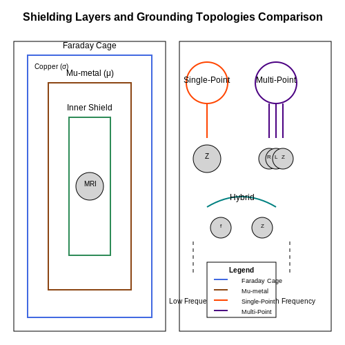
Practical shielding materials include copper (high σ) for electric fields and mu-metal (high μ) for magnetic fields below 100 kHz.
Grounding Topologies
Grounding strategies must address both safety and signal integrity:
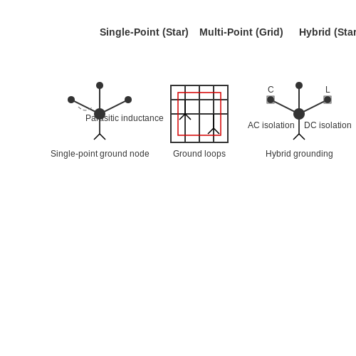
- Single-point grounding: Optimal for low-frequency circuits (<100 kHz) to prevent ground loops
- Multi-point grounding: Required for high-frequency systems (>10 MHz) to minimize ground impedance
- Hybrid grounding: Uses capacitors/inductors to create frequency-selective paths
The ground impedance Zg must be minimized, particularly the inductive component:
where L ≈ 10 nH/cm for typical PCB traces. At 100 MHz, even 1 cm of trace adds 6Ω reactance.
Practical Implementation
For mixed-signal systems:
- Partition analog and digital grounds, connecting at a single point near the power supply
- Use star grounding for sensitive analog circuits
- Implement guard rings around high-impedance nodes with driven shields
In RF circuits, ground planes must be continuous with via stitching (<1/20λ spacing). For a 2.4 GHz design, this requires vias every 6 mm on FR4 substrate.
Case Study: MRI Shielding
MRI rooms use nested shields: a copper Faraday cage (δ = 66 μm at 64 MHz) for RF attenuation inside a mu-metal layer for static field containment. The door gasket design achieves >100 dB attenuation through finger stock contacts maintaining continuous conductivity.
2.2 Filtering with Passive Components
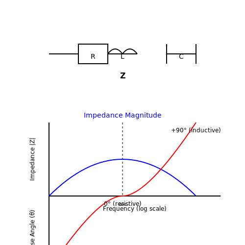
Passive filters, constructed using resistors (R), capacitors (C), and inductors (L), remain fundamental tools for noise suppression in circuits. Unlike active filters, they require no external power and exhibit superior reliability in high-frequency applications. The effectiveness of these filters is governed by their frequency-dependent impedance characteristics, which attenuate unwanted noise while preserving signal integrity.
First-Order RC Low-Pass Filter
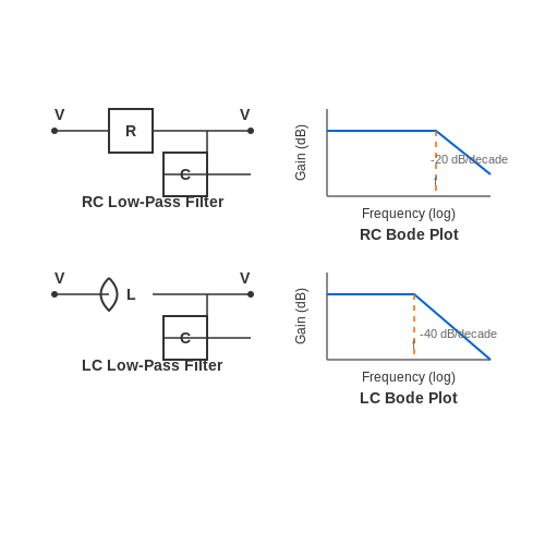
The simplest passive noise filter is the first-order RC low-pass network, where the capacitor shunts high-frequency noise to ground. The transfer function H(f) of this configuration is derived from voltage division:
The cutoff frequency fc, where the signal attenuates by -3 dB, occurs when the capacitive reactance equals the resistance:
In practice, this filter provides a roll-off of -20 dB/decade above fc. For instance, a 1 kΩ resistor paired with a 100 nF capacitor yields a cutoff at 1.59 kHz, effectively suppressing switching noise from digital clocks while passing analog signals below this threshold.
LC Filters for High-Frequency Isolation
When dealing with RF interference or power supply ripple, LC filters offer steeper attenuation slopes. The second-order LC low-pass filter has a transfer function:
Key considerations include:
- Self-resonant frequency of components limiting effective filtering range
- Q-factor affecting peaking near cutoff:
$$ Q = \frac{1}{R}\sqrt{\frac{L}{C}} $$
- Parasitic ESR in capacitors causing additional insertion loss
Practical Implementation Guidelines
Optimal noise suppression requires careful component selection:
| Parameter | Capacitor Type | Inductor Type |
|---|---|---|
| Low-frequency (<100 kHz) | Electrolytic | Toroidal ferrite |
| Medium-frequency (100 kHz-10 MHz) | Ceramic X7R | Shielded drum core |
| High-frequency (>10 MHz) | NP0/C0G ceramic | Air core or planar |
Placement significantly impacts performance - filters should be positioned as close as possible to noise sources. For power lines, a π-filter (C-L-C) configuration provides superior broadband attenuation, while differential mode noise in signal lines often requires common-mode chokes with carefully matched capacitance.
Frequency-Domain Analysis
The effectiveness of passive filters is best analyzed through Bode plots. For an RC filter, the magnitude response in decibels is:
At frequencies significantly above fc, this simplifies to approximately -20 dB/decade. When cascading multiple filter stages, the total attenuation becomes the sum of individual stage attenuations, though component interactions may alter the expected response due to impedance mismatches.
Proper PCB Layout for Noise Minimization
Ground Plane Design
A solid ground plane is critical for minimizing noise in high-frequency circuits. The ground plane acts as a low-impedance return path for signals and helps reduce electromagnetic interference (EMI). For multilayer PCBs, dedicate at least one full layer to the ground plane. The ground plane's effectiveness can be quantified by its impedance, which follows:
where ρ is the resistivity of the copper, t is the thickness, A is the area, and L is the parasitic inductance. A larger ground plane reduces both resistive and inductive components of impedance.
Signal Routing Strategies
Differential signaling and controlled impedance routing are essential for noise immunity. For high-speed signals:
- Route differential pairs closely together to maintain coupling and reject common-mode noise.
- Minimize trace length to reduce parasitic inductance and capacitance.
- Avoid right-angle bends, which can cause impedance discontinuities and reflections.
The characteristic impedance Z0 of a microstrip trace is given by:
where εr is the dielectric constant, h is the height above the ground plane, w is the trace width, and t is the trace thickness.
Power Distribution Network (PDN) Optimization
A well-designed PDN minimizes voltage fluctuations and suppresses switching noise. Key techniques include:
- Use multiple vias to connect power and ground planes, reducing inductance.
- Place decoupling capacitors close to IC power pins to minimize loop area.
- Employ bulk capacitors for low-frequency noise suppression and smaller ceramics for high frequencies.
The effective impedance of the PDN can be approximated by:
Component Placement and Shielding
Sensitive analog components should be placed away from high-speed digital sections. When unavoidable, shielding techniques such as:
- Guard rings around sensitive traces to divert noise.
- Faraday cages for RF-sensitive components.
- Partitioning ground planes to prevent digital noise from coupling into analog sections.
The effectiveness of shielding depends on the skin depth δ:
where μ is the permeability and ρ is the resistivity of the shielding material.
3. Differential Signaling and Balanced Circuits
Differential Signaling and Balanced Circuits
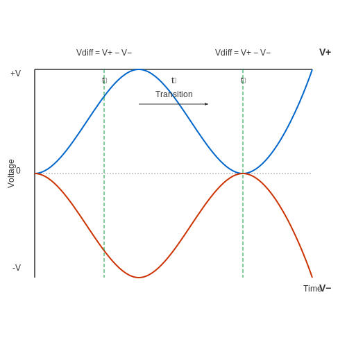
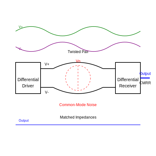
Differential signaling is a noise-resistant technique where a signal is transmitted as the difference between two complementary voltages (V+ and V-) over a pair of conductors. Common-mode noise, which couples equally onto both lines, is rejected at the receiver by subtracting the two signals. The key metric is the common-mode rejection ratio (CMRR), defined as:
where Ad is the differential gain and Ac is the common-mode gain. High CMRR (>60 dB) is critical in environments with electromagnetic interference (EMI), such as industrial motor control or medical instrumentation.
Mathematical Analysis of Noise Rejection
Consider a differential pair with signals V1 and V2 corrupted by common-mode noise Vn:
The differential receiver outputs:
For ideal rejection (Ac = 0), the noise term vanishes. Practical implementations achieve this through:
- Matched impedances (ΔZ/Z < 1%) to prevent common-to-differential conversion
- Twisted-pair wiring to ensure equal noise coupling
- High-performance op-amps with CMRR > 100 dB
Balanced Circuit Implementations
Balanced interfaces use three key components:
- Differential driver: Converts single-ended to differential signals (e.g., Texas Instruments THS4531)
- Transmission line: 100Ω twisted pair for RF applications, shielded CAT6 for audio
- Differential receiver: Instrumentation amplifier (INA141) or transformer-coupled input
Case Study: Audio Transmission
Professional audio systems (AES3, XLR) use differential signaling to maintain signal integrity over 100-meter cable runs. The EIA-422 standard specifies:
- Voltage swing: ±2V differential
- Max skew: 0.1 UI (unit interval)
- Termination: 110Ω ±10%
Measurements show a 40 dB reduction in 60 Hz hum compared to unbalanced connections when tested under 1 V/m RF field (IEC 61000-4-3).
High-Speed Digital Applications
LVDS (ANSI/TIA/EIA-644) leverages differential signaling for multi-Gbps data transmission. The eye diagram integrity is maintained by:
Differential PCB routing requires:
- Controlled impedance (100Ω differential, 50Ω single-ended)
- Length matching (ΔL < 5 mil for 10 Gbps)
- Ground plane continuity
3.2 Noise Cancellation Using Active Filters
Active filters leverage operational amplifiers (op-amps) to achieve precise noise cancellation by selectively attenuating undesired frequency components while preserving the signal of interest. Unlike passive filters, active filters provide gain and high input impedance, minimizing loading effects and improving signal integrity. The design of these filters hinges on the transfer function, which dictates the frequency response and roll-off characteristics.
Transfer Function and Frequency Response
The transfer function H(s) of an active filter defines its behavior in the Laplace domain, where s = jω. For a second-order low-pass active filter, the transfer function is:
Here, K is the DC gain, ω₀ is the cutoff frequency, and Q is the quality factor, which determines the sharpness of the roll-off. A higher Q results in a steeper transition band but may introduce ringing in the time domain.
Topologies for Noise Cancellation
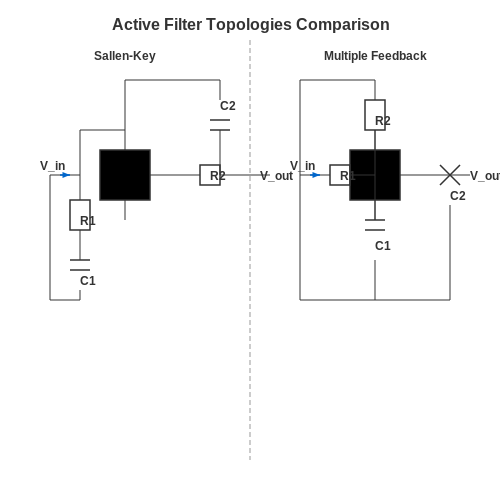
Sallen-Key Filter
The Sallen-Key configuration is widely used for its simplicity and stability. It employs an op-amp in a non-inverting configuration with a feedback network of resistors and capacitors. The cutoff frequency and Q are given by:
where K = 1 + R_f / R_g is the gain set by the feedback resistors. Proper selection of component values ensures optimal noise suppression without destabilizing the filter.
Multiple Feedback (MFB) Filter
The MFB topology offers inverting gain and improved stability for high-Q applications. Its transfer function is:
This design is particularly effective for band-pass and notch filters, where precise control over the center frequency and bandwidth is critical for noise cancellation.
Practical Considerations
Active filters are sensitive to component tolerances and op-amp non-idealities, such as finite gain-bandwidth product and slew rate. For instance, a Butterworth response requires Q = 0.707 for maximal flatness, but parasitic capacitances can alter this value. Monte Carlo simulations are often employed to assess robustness against component variations.
In high-frequency applications, the op-amp's phase margin must be sufficient to prevent oscillations. A compensation capacitor may be added to mitigate this, though it reduces the filter's bandwidth. For example, a 10 MHz cutoff filter might require an op-amp with at least 100 MHz gain-bandwidth product to maintain accuracy.
Applications in Noise-Sensitive Systems
Active filters are integral to medical instrumentation, where 50/60 Hz power-line interference must be rejected without distorting bioelectric signals. A twin-T notch filter with an active feedback loop can achieve >40 dB attenuation at the target frequency. Similarly, in audio systems, active high-pass filters remove DC offsets and low-frequency rumble before amplification.
3.3 Feedback Techniques for Noise Suppression
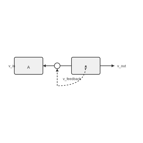
Feedback mechanisms are fundamental in reducing noise in electronic circuits by leveraging closed-loop control to stabilize signal integrity. The two primary feedback topologies—negative feedback and positive feedback—exhibit distinct noise-suppression characteristics. Negative feedback is widely employed for its ability to linearize amplifier responses and minimize distortion, while positive feedback, though less common in noise reduction, finds niche applications in oscillators and active filtering.
Negative Feedback and Noise Reduction
The noise suppression capability of negative feedback arises from its ability to reduce the effective gain of the amplifier while improving linearity. Consider an amplifier with open-loop gain A and feedback factor β. The closed-loop gain ACL is given by:
For large A, this simplifies to ACL ≈ 1/β, making the system less sensitive to variations in A due to noise or component tolerances. The input-referred noise voltage vn is similarly attenuated by the loop gain 1 + Aβ:
Practical implementations often employ operational amplifiers (op-amps) in feedback configurations such as:
- Inverting amplifier: Noise at the input is suppressed by the feedback network's impedance ratio.
- Non-inverting amplifier: Exhibits high input impedance, reducing susceptibility to coupled noise.
- Transimpedance amplifier: Converts current noise to a voltage signal, which is then filtered by the feedback loop.
Stability Considerations in Feedback Systems
While negative feedback reduces noise, it introduces stability challenges due to phase shifts at high frequencies. The Barkhausen stability criterion dictates that oscillations occur if the loop gain satisfies:
To mitigate instability, engineers employ compensation techniques such as:
- Dominant pole compensation: Introduces a low-frequency pole to ensure a -20 dB/decade rolloff before the unity-gain frequency.
- Miller compensation: Uses a capacitor across high-gain stages to reduce bandwidth and improve phase margin.
- Lead-lag compensation: Combines resistive and capacitive elements to shape the frequency response.
Case Study: Feedback in Low-Noise Amplifiers (LNAs)
In RF applications, LNAs utilize feedback to achieve sub-nV/√Hz noise figures. A common topology is the cascode amplifier with inductive degeneration, where feedback:
- Linearizes the transconductance (gm) of the input transistor.
- Minimizes Miller effect at high frequencies.
- Provides impedance matching for optimal noise power transfer.
The noise factor F of such an amplifier is derived from the Friis formula:
where Fmin is the minimum achievable noise figure, Rn is the equivalent noise resistance, and Ys, Yopt are the source and optimal admittances, respectively.
Active Filtering via Feedback
Feedback enables the implementation of active filters with precise cutoff frequencies and quality factors. A second-order Sallen-Key low-pass filter, for instance, uses feedback to set its characteristic frequency f0 and quality factor Q:
where K is the amplifier gain. Proper selection of component values ensures minimal noise peaking while maintaining desired rolloff characteristics.
4. Digital Signal Processing for Noise Reduction
4.1 Digital Signal Processing for Noise Reduction
Digital signal processing (DSP) techniques are widely used to mitigate noise in circuits by leveraging computational algorithms to filter, enhance, or reconstruct signals. Unlike analog filtering, DSP provides precise control over frequency response, phase characteristics, and adaptive noise suppression.
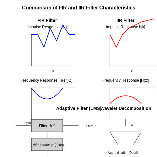
Finite Impulse Response (FIR) Filters
FIR filters are characterized by their finite-duration impulse response, making them inherently stable and linear-phase. The output y[n] of an FIR filter is computed as the weighted sum of past and present input samples:
where h[k] represents the filter coefficients, x[n-k] are the input samples, and N is the filter order. The frequency response is determined by the Fourier transform of h[k]:
FIR filters are particularly effective in removing high-frequency noise while preserving signal integrity. Windowing techniques (e.g., Hamming, Blackman) are often applied to minimize spectral leakage.
Infinite Impulse Response (IIR) Filters
IIR filters incorporate feedback, enabling sharper roll-off characteristics with fewer coefficients compared to FIR filters. The difference equation for an IIR filter is:
where b_k and a_k are feedforward and feedback coefficients, respectively. The transfer function in the z-domain is:
IIR filters are computationally efficient but require careful design to avoid instability due to pole placement near the unit circle.
Adaptive Filtering
Adaptive filters dynamically adjust coefficients to minimize noise based on real-time signal statistics. The Least Mean Squares (LMS) algorithm is a widely used approach:
where w[n] are the filter weights, μ is the step size, e[n] is the error signal, and x[n] is the input vector. Applications include echo cancellation, biomedical signal processing, and noise suppression in communication systems.
Wavelet Transform Denoising
Wavelet transforms decompose signals into time-frequency components, allowing localized noise removal. The discrete wavelet transform (DWT) is defined as:
where ψ is the mother wavelet, and j, k are scaling and translation parameters. Thresholding wavelet coefficients (e.g., soft or hard thresholding) effectively suppresses noise while preserving transient features.
Real-World Applications
- Audio Processing: FIR/IIR filters remove hiss and hum in audio signals.
- Medical Imaging: Wavelet denoising enhances MRI and ECG signals.
- Telecommunications: Adaptive filters mitigate channel noise in 5G and OFDM systems.
4.2 Adaptive Noise Cancellation Techniques
Adaptive noise cancellation (ANC) leverages adaptive filtering to dynamically suppress interference in real-time. Unlike fixed filters, ANC systems adjust their parameters based on the noise characteristics, making them highly effective in non-stationary environments.
Principle of Adaptive Noise Cancellation
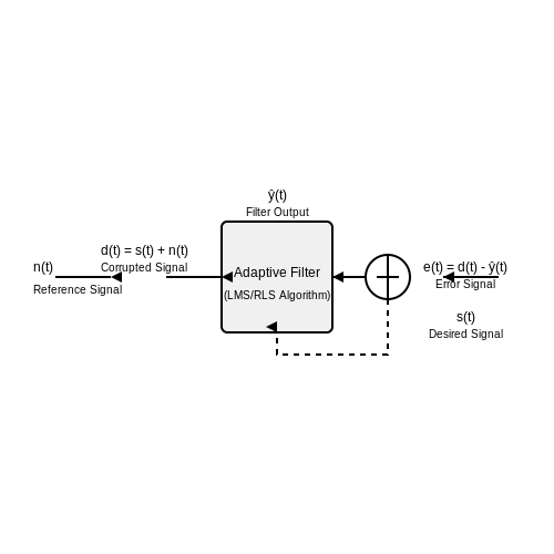
The core idea relies on a reference signal n(t), correlated with the noise but independent of the desired signal s(t). The adaptive filter generates an estimate ŷ(t) of the noise, which is subtracted from the corrupted signal d(t) = s(t) + n(t) to produce the error signal e(t):
The error signal drives the adaptation process, typically via the Least Mean Squares (LMS) or Recursive Least Squares (RLS) algorithms, minimizing the mean square error.
LMS Algorithm Derivation
The LMS algorithm updates the filter weights w iteratively:
where μ is the step size, e(n) is the error, and x(n) is the reference input vector. The stability criterion requires:
with λmax being the largest eigenvalue of the input autocorrelation matrix.
Applications and Practical Considerations
- Biomedical Signal Processing: Removing 50/60 Hz powerline interference from ECG/EEG signals.
- Acoustic Noise Cancellation: Active noise-canceling headphones use ANC to attenuate ambient noise.
- Communication Systems: Mitigating narrowband interference in broadband signals.
Challenges include convergence speed versus steady-state error trade-offs and computational complexity in high-order filters.
Case Study: ANC in Hearing Aids
Modern hearing aids employ multi-channel ANC with frequency-domain adaptive filters (FDAF) to handle non-stationary noise. The system decomposes the input into subbands, allowing parallel processing and faster adaptation.
where N is the frame length in the short-time Fourier transform (STFT) implementation.
4.3 EMI/RFI Mitigation Strategies
Shielding Techniques
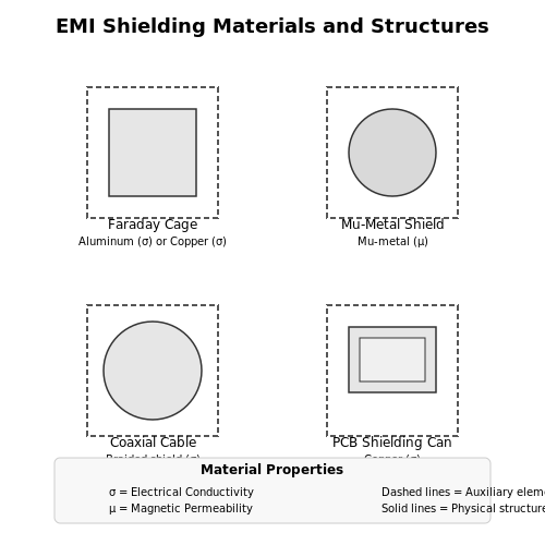
Electromagnetic interference (EMI) and radio-frequency interference (RFI) can severely degrade circuit performance. Shielding involves enclosing sensitive components or entire circuits within conductive or magnetic materials to block external fields. The effectiveness of shielding depends on the material's permeability (μ) and conductivity (σ). For high-frequency EMI, Faraday cages made of copper or aluminum are common, while mu-metal shields excel at low-frequency magnetic interference.
Practical applications include coaxial cables with braided shields and PCB-level shielding cans. The skin effect dictates that higher frequencies attenuate more rapidly, making material thickness less critical above 1 MHz.
Filtering Methods
Passive filtering is a cornerstone of EMI suppression. Common-mode chokes, ferrite beads, and LC filters attenuate unwanted frequencies while preserving signal integrity. The insertion loss (IL) of a filter is given by:
For power lines, π-filters with X/Y capacitors and inductors are standard. Differential-mode noise is mitigated with series inductors, while common-mode noise requires chokes with high impedance at the interference frequency.
Grounding and Layout Optimization
Proper grounding minimizes ground loops, a major source of EMI. Star grounding and ground planes reduce impedance paths for high-frequency currents. On PCBs, techniques include:
- Partitioning: Separating analog, digital, and RF sections.
- Minimizing loop areas: Reducing the area of current return paths decreases magnetic coupling.
- Using vias: Shortening return paths for high-speed signals.
Component Selection and Decoupling
High-frequency decoupling capacitors (typically 0.1 μF ceramic) placed near IC power pins suppress transient currents. The resonant frequency of a decoupling network is critical:
Low-ESR capacitors and distributed bulk capacitance (10–100 μF) further stabilize power rails. Ferrite beads in series with power lines add frequency-dependent impedance.
Active Cancellation Techniques
Active noise cancellation (ANC) injects an anti-phase signal to destructively interfere with EMI. Adaptive algorithms, such as LMS (Least Mean Squares), dynamically adjust cancellation signals:
Applications include audio systems and power line communications, where passive methods are insufficient.
Real-World Case Study: Switching Power Supplies
In a 100 W buck converter, EMI arises from high di/dt loops. Mitigation strategies include:
- Snubber circuits: RC networks dampen ringing across MOSFETs.
- Spread-spectrum clocking: Modulating the switching frequency reduces peak emissions.
- Shielded inductors: Containing magnetic flux leakage.
5. Key Research Papers on Noise Reduction
5.1 Key Research Papers on Noise Reduction
- (PDF) Various Noise Sources & Noise Reduction Techniques ... - ResearchGate — The overall performance of the circuit is entirely dependent on its noise characteristics. ... Noise Reduction Techniques V.5.0 May 2013.pdf ... on elimination of noise by electronic grounding of ...
- Lecture Notes in Analog Electronics: Noise in Electronic Circuits and ... — The number of types of noise sources in electronics is almost unlimited. The book offers unique comprehensive approach to noise analysis in electronic circuits based on modified nodal analysis and the superposition theorem. It also encompasses a broadest set of low noise amplifier design procedures covering BJT, MOSET, MESFET, and HEMT ...
- PDF TEM Cell Testing of Cable Noise Reduction Techniques from 2 MHz to 200 ... — There are numerous papers and textbooks that present theoretical analyses of cable noise reduction techniques. However, empirical data is often targeted to low frequencies (e.g. <50 KHz) or high frequencies (>100 MHz). Additionally, a comprehensive study showing the relative effects of various noise reduction techniques is needed.
- Noise Reduction - SpringerLink — 5.1.1.1 Separation of Airborne and Structure-Borne Sound. For the development of constructive noise reduction measures, it is necessary to determine the airborne and structure-borne sound radiation of a machine or system or its share in the total sound radiation in a quantitative way.
- PDF Design techniques to improve noise and linearity of data converters — Design Techniques to Improve Noise and Linearity of Data Converters A Dissertation Presented by ... 4 Noise Reduction Technique Through Bandwidth Switching 39 ... 4.3 Circuit model for noise analysis of the conventional THA during the amplification
- PDF Passive Cancellation Main - Virginia Tech — In this thesis a survey of CM noise reduction techniques is presented, encompassing conventional and active cancellation techniques. The new method for passive noise cancellation is presented, which is then applied to families of isolated DC/DC converters, non-isolated DC/DC converters, and DC/AC inverters and motor drives.
- PDF Active Noise Cancellation using Adaptive Filter Algorithms — noise (the "target" noise) that would like to reduce, by producing an anti-noise which cancels out the noise component by the method of adaptive filtering. Therefore, the main aim of ANC system is to reduce the noise component from the signal of interest. Figure 1 shows schematic diagram of a single channel feedback ANC system
- A grid-based nonlinear approach to noise reduction and deconvolution ... — This paper described novel approaches to perform (1) a grid-based nonlinear noise reduction and (2) deconvolution of underresolved measurements to reveal the underlying time-resolved signal, when reference data representing the dynamics of system were available along with noisy time-series data from the same system.
- PDF A Review of Offset and Noise Reduction Techniques for ... - ResearchGate — Fig. 2: Noise PSD reduction as a result of auto-zero. Journal of Integrated Circuits and Systems, vol. 17, n.1, 2022 3 The auto-zero technique is more efficient when the
- Review of Offset and Noise Reduction Techniques for CMOS - ResearchGate — This paper reviews some the most relevant techniques applied to reducing input errors of CMOS amplifiers aiming at to provide a condensed set of information that can help designers at the starting ...
5.2 Recommended Books on Circuit Noise
- PDF Low Noise Signal Conditioning for Sensor-Based Circuits - Analog — conditioning circuits and raise awareness for selecting appropriate parts. Noise in Signal Conditioning Circuits Noise can be separated into two distinct categories, extrinsic (interference) and intrinsic (inherent). Electrical and magnetic noise are forms of extrinsic noise. They can be periodic, intermittentor random, . System designers can
- PDF Please note that the links in the P logotype above are "live" — Earlier ed. published under title: Noise reduction techniques in electronic systems, 1988. Includes bibliographical references and index. ISBN 978--470-18930-6 1. Electronic circuits-Noise. 2. Electromagnetic compatibility. I. Ott, Henry W., 1936- Noise reduction techniques in electronic systems. II. Title. TK7867.5.O867 2009 621.382u24 ...
- Lecture Notes in Analog Electronics: Noise in Electronic Circuits and ... — The number of types of noise sources in electronics is almost unlimited. The book offers unique comprehensive approach to noise analysis in electronic circuits based on modified nodal analysis and the superposition theorem. It also encompasses a broadest set of low noise amplifier design procedures covering BJT, MOSET, MESFET, and HEMT ...
- Electromagnetic Compatibility Engineering | Noise in Electronic Systems ... — Praise for Noise Reduction Techniques IN electronic systems Henry Ott has literally written the book on the subject of EMC. . . . He not only knows the subject, but has the rare ability to communicate that knowledge to others. —EE Times Electromagnetic Compatibility Engineering is a completely revised, expanded, and updated version of Henry Otts popular book Noise Reduction Techniques in ...
- PDF CHAPTER 5 Chopping: a technique for noise and offset reduction — The first term take s care for 1/f noise and offset reduction. The simple switched current memory cell from Chapter 3 has also autozero properties and therefore flicker noise is reduced. In conclusion, autozero amplifiers will reduce the offset and 1/f noise by using sampling techniques at the expense of increasing the white noise in the baseband.
- 5.2 Electronic Noise Modeling - SpringerLink — Figure 5.2.1.1b depicts the spectral density of the thermal noise current which will be subject of our interest later on. The total instantaneous value of the current through the semiconductor sample is the sum of the thermal and drift values. Bearing in mind that the drift current is incomparably higher, in the usual analysis of electrical circuits, the thermal component is ignored which is ...
- Electronics/Noise in electronic circuits - Wikibooks, open books for an ... — Differential signaling is a method of transmitting information electrically by means of two complementary signals sent on two separate wires. The technique can be used for both analogue signaling, as in some audio systems, and digital signaling, as in RS-422, RS-485, PCI Express and USB.
- Electromagnetic Compatibility Engineering | Wiley — Praise for Noise Reduction Techniques IN electronic systems "Henry Ott has literally 'written the book' on the subject of EMC. . . . He not only knows the subject, but has the rare ability to communicate that knowledge to others." — EE Times Electromagnetic Compatibility Engineering is a completely revised, expanded, and updated version of Henry Ott's popular book Noise Reduction Techniques ...
- (PDF) Various Noise Sources & Noise Reduction Techniques ... - ResearchGate — Noise may be internally generated within the system i.e., within the circuit when we call it internal noise or the source may be external when we call it an external noise (Attri, R. K., 1998 ...
- Engineering Noise Control, Fifth Edition - ResearchGate — For those who are already well versed in the art and science of noise control, the book will provide an extremely useful reference. A wide range of example problems that are linked to noise ...
5.3 Online Resources and Tutorials
- 5.3 Electronic Noise Analysis in Basic Circuits - Springer — 5.3 Electronic Noise Analysis in Basic Circuits 5.3.1 CS and CE Amplifier with Degenerated Source/Emitter Figure 5.3.1a depicts the schematic of the CS amplifier whose simplified low frequency noise equivalent circuit is depicted in Fig. 5.3.1b. The following system of nodal equations holds for this circuit:
- PDF CHAPTER 5 Chopping: a technique for noise and offset reduction — The first term take s care for 1/f noise and offset reduction. The simple switched current memory cell from Chapter 3 has also autozero properties and therefore flicker noise is reduced. In conclusion, autozero amplifiers will reduce the offset and 1/f noise by using sampling techniques at the expense of increasing the white noise in the baseband.
- PDF Practical Shielding, EMC/EMI, Noise Reduction, Earthing and Circuit ... — Practical Shielding, EMC/EMI, Noise Reduction, Earthing and Circuit Board Layout Contents 1 Introduction 1 1.1 Introduction 1 1.2 EMI vs EMC 3 1.3 Interference sources 3 1.4 Need for standards 5 1.5 EMC - the issues 6 1.6 Electromagnetic disturbances 7 1.7 EMC testing categories 8 1.8 The compatibility gap 9
- PDF Noise and Noise Reduction - Purdue University — Noise Sources •Flicker Noise Low‐frequency noise, including random drift, occurs in near all electronic devices, and can show up with a variety of other effects, such as impurities in a conductive channel, generation and recombination noise in a transistor due to base current, and so on
- Practical Shielding, EMC/EMI, Noise Reduction, Earthing and Circuit ... — 1.1 Introduction. Electromagnetic Compatibility (EMC) is defined as the ability of a device, equipment or a system to function satisfactorily in its electromagnetic environment without introducing intolerable electromagnetic disturbance to anything in that environment.Any electronic equipment is both capable of emitting unintended signals (i.e., interference to other electronic equipment) and ...
- 5.3 Electronic Noise Analysis in Basic Circuits — 5.3.7.1 Noise in General Feedback Amplifier. Let at the input to the feedback amplifier of Fig. 5.3.15a together with the useful signal x in acts a noise signal denoted x nin. There is no reason not to amplify the noise signal as much as the useful signal.
- Lecture Notes in Analog Electronics: Noise in Electronic Circuits and ... — The number of types of noise sources in electronics is almost unlimited. The book offers unique comprehensive approach to noise analysis in electronic circuits based on modified nodal analysis and the superposition theorem. It also encompasses a broadest set of low noise amplifier design procedures covering BJT, MOSET, MESFET, and HEMT ...
- PDF On-Chip Power Noise Reduction Techniques High Performance SoC-Based ... — digital circuits. The Quiet Gnd denotes a noise-free ground for the noise sensitive circuits. The dependence of the noise reduction on physical sep-aration between the noisy and noise sensitive circuits is presented in subsection Ill-A. Thesensitivity ofthe proposed technique to frequency andcapacitance variations is discussed in subsection III-B.
- PDF Methods of noise reduction - EPFL — Reduction in thermal noise voltage Reduction in capacitive interference coupling (see later) Example: Using 20 kHz bandwidth, a 1 MΩ sample at room temperature generates thermal noise of 20 µV. Reducing the resistance to 10 kΩ would reduce it to 2 µV. The best case: superconductors (R s = 0), metallic samples (low R s)
- Various Noise Sources & Noise Reduction Techniques in ... - ResearchGate — Noise may be internally generated within the system i.e., within the circuit when we call it internal noise or the source may be external when we call it an external noise (Attri, R. K., 1998 ...