DC-DC Boost Converter
1. Basic Principles of DC-DC Conversion
1.1 Basic Principles of DC-DC Conversion
At the heart of many modern electronic systems lies the necessity for efficient power management. The DC-DC boost converter exemplifies a critical component used to convert and regulate voltage levels in a variety of applications, from portable electronics to renewable energy systems. Understanding the fundamental principles behind DC-DC conversion not only aids in the design of reliable power electronics but also enhances efficiency in various practical applications.
DC-DC conversion involves the transformation of a direct current (DC) voltage level to a higher one using an inductor, switches (typically transistors), a diode, and a capacitor. This process can be described in terms of magnetic energy storage and release, which is central to the operation of any boost converter.
The Principle of Energy Conservation
To comprehend how a boost converter operates, it’s crucial to acknowledge the principle of energy conservation. In a boost converter, energy input to the system must equal the energy output, minus any losses due to inefficiencies. This can be expressed mathematically as:
Where:
- Pin is the input power
- Pout is the output power
- V denotes voltage
- I denotes current
Whereby, with ideal conditions, voltage and current are related through:
Here, D represents the duty cycle, defined as the ratio of the time the switch is closed to the total switching period. As the duty cycle increases, the output voltage escalates proportionally, allowing for a higher voltage than the input. Understanding this relationship is vital for engineers when designing circuits for specific requirements.
Operation of a Boost Converter
The operational principle of a boost converter can be simplified into two distinct phases:
- Phase 1 (Charging): The switch is closed, and the input voltage Vin is applied to the inductor. During this phase, the inductor is charged, storing energy in the form of a magnetic field. The current through the inductor increases, causing the voltage across it to rise, while a small amount of current is drawn from the input supply.
- Phase 2 (Discharging): When the switch is opened, the inductor opposes the sudden drop in current by releasing its stored energy. This stored energy adds to the input voltage, raising the output voltage Vout delivered to the load. The diode prevents the output capacitor from discharging back into the inductor during this phase, ensuring a stable output voltage.
The overall efficiency of a boost converter is influenced by various factors, including the switching frequency, inductor size, and choice of semiconductor devices. Historically, boost converters have been instrumental in the evolution of portable and renewable energy systems, serving as a cornerstone for battery-operated devices and solar applications.
In conclusion, the basic principles behind DC-DC boost conversion intertwine with fundamental physics regarding energy storage and conversion. Grasping these concepts is crucial for advanced engineers and researchers aiming to optimize and innovate in the field of power electronics.
1.2 The Boost Converter Concept
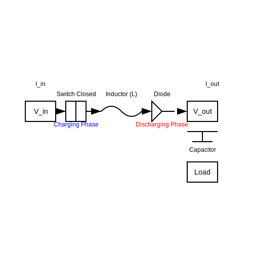
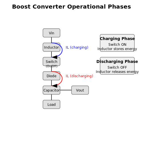
The DC-DC boost converter is an essential component in modern electronic systems, widely applied in various industries, including renewable energy, portable electronics, and electric vehicles. This converter stands out due to its simplicity and efficiency in stepping up a lower DC voltage to a higher DC voltage. At the heart of the boost converter is the interaction between inductors, capacitors, and switching devices, typically transistors. The operation of a boost converter can be understood by examining two main states: the charging state and the discharging state of the inductor.Inductor Charging Phase
In the charging phase, the switching device is in the ‘on’ state, allowing current to flow through the inductor. During this time, the inductor stores energy in the form of magnetic flux. The input voltage (\(V_{in}\)) contributes to the inductor voltage (\(V_L\)) as follows:Inductor Discharging Phase
Upon transitioning to the discharging phase, the switch opens. The energy stored in the inductor is now released, and the inductor is connected to the output capacitor and load. The key characteristic during this phase is that the inductor reverses its polarity, adding voltage to the input:Practical Applications and Relevance
The boost converter finds broad applications in scenarios where stepping up voltage is critical. For instance:- Battery-Powered Devices: Devices such as smartphones and tablets utilize boost converters to manage battery voltage while ensuring consistent performance.
- Solar Energy Systems: In photovoltaic systems, boost converters are employed to optimize the output from solar panels, ensuring that the energy harvested is maximized.
- LED Drivers: For high-power LED applications, where precise voltage levels are crucial for performance, boost converters enable effective power conversion.
2. Key Components of a Boost Converter
2.1 Key Components of a Boost Converter
The fundamental operation of a DC-DC boost converter relies on several key components. Understanding the characteristics and functions of these components is essential for designing efficient power conversion systems. The primary components include the inductor, switching device, diode, output capacitor, and control circuit. Each plays a critical role in the conversion process, transforming a lower DC voltage into a higher output voltage.Inductor
The inductor is arguably the most critical component of a boost converter. It stores energy in its magnetic field when current passes through it. In a typical boost converter configuration, the inductor is connected to the input voltage source, and during this charging period, it accumulates energy. The energy stored can be quantified by the equation:Switching Device
Next, the switching device—commonly a MOSFET or BJT—controls the flow of current through the inductor. By periodically closing and opening, the switch regulates the energy transfer to the inductor. The switching frequency impacts the efficiency and size of the converter. An increase in frequency can lead to a reduction in inductor size; however, it can also result in higher switching losses and reduced efficiency. The efficiency of the switching operation can be analyzed using the following relationship:Diode
The diode in a boost converter acts as a one-way valve, permitting current to pass from the inductor to the output capacitor while blocking any reverse flow. This component is essential for ensuring that the energy transfer from the inductor occurs effectively when the switching device is turned off. The selection of the diode is crucial; it must be capable of handling the peak reverse voltage and forward current. Schottky diodes are often preferred due to their fast switching speeds and lower forward voltage drop, resulting in higher efficiency.Output Capacitor
The output capacitor serves to smooth the output voltage and filter out voltage ripples caused by the switching of the converter. The capacitance value must be chosen carefully to provide adequate smoothing without introducing unacceptable transient response characteristics. The voltage ripple can be calculated with the formula:Control Circuit
Finally, the control circuit, often implemented using a dedicated controller IC, regulates the duty cycle of the switching device. By adjusting the amount of time the switch is closed versus open, the control circuit maintains the desired output voltage regardless of input variations and load changes. Advanced control techniques, such as pulse-width modulation (PWM) and voltage mode control, enhance performance, allowing for improved efficiency and stability. Understanding these key components not only aids in optimizing boost converter designs but also provides a solid foundation for exploring various applications ranging from portable electronics to renewable energy systems where efficient power management is critical. As engineers and researchers delve deeper into boost converter technology, innovations continue to arise, driving performance enhancements and expanding the potential applications of these essential devices.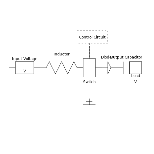
2.2 Circuit Topology of a Boost Converter
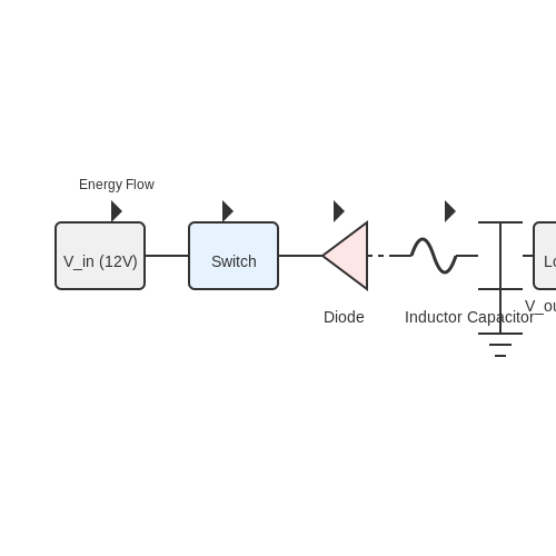
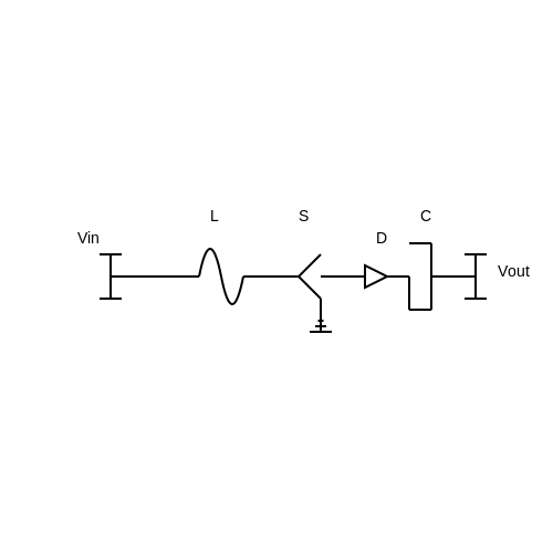
Understanding the circuit topology of a DC-DC boost converter is essential to grasp how it effectively increases voltage levels. At its core, a boost converter operates on the principles of energy storage and conversion, primarily utilizing an inductor, a switch (usually a transistor), a diode, and a capacitor.
The basic configuration of a boost converter involves placing these components in a specific arrangement to enable the conversion of a lower voltage input to a higher voltage output. This is achieved by controlling the switching mechanism, thus managing energy transfer in a periodic manner. Let's delve deeper into the individual components and their functionalities.
Key Components and Their Functions
- Inductor: The inductor stores energy when the switch is closed. It plays a critical role in the energy conversion process by creating a magnetic field that subsequently releases energy when the switch opens.
- Switch: Typically a transistor, the switch periodically connects and disconnects the inductor to the power supply, enabling the controlled transfer of energy.
- Diode: The diode allows current to flow in only one direction, effectively directing the stored energy from the inductor to the output capacitor during the switch's off state.
- Capacitor: The capacitor intersects and smooths the output voltage to ensure a stable supply to the load, accumulating charge when the diode is forward-biased and providing energy during demand spikes.
Basic Operation of the Boost Converter
The operation of a boost converter can be understood in two distinct phases—when the switch is closed and when it is open:
Phase 1: Switch Closed
During this phase, the switch connects the input voltage to the inductor. The inductor starts to store energy, which increases the current flowing through it. The energy (\(E_L\)) stored in the inductor can be expressed as:
where \(L\) is the inductance, and \(I\) is the current through the inductor.
Phase 2: Switch Open
When the switch opens, the inductor attempts to maintain the current by inducing a voltage across its terminals, which adds to the input voltage. This leads to a higher voltage across the output. The output voltage (\(V_{out}\)) can be described relative to the input voltage (\(V_{in}\)) as:
where \(D\) is the duty cycle, a ratio of the duration the switch is closed to the total switching period.
This inherent property of voltage multiplication makes boost converters extremely useful in various applications, notably in renewable energy systems such as solar power, battery-powered devices, and electric vehicles where efficient voltage conversion is pivotal.
Real-World Applications
As engineers and physicists work toward enhancing energy efficiency and sustainability, applications of boost converters are ever-expanding:
- Portable Electronics: Boost converters are critical in devices such as portable chargers and digital cameras, where battery voltages need to be stepped up to power various components.
- LED Drivers: For powering LED lights that require higher voltages, boost converters allow for an efficient and effective power supply solution.
- Power Management in Electric Vehicles: Boost converters play a significant role in the management of power distribution to various subsystems in electric vehicles, ensuring that each component receives the appropriate voltage.
In summary, the topology of a DC-DC boost converter is a vital concept in electrical engineering, rooted in fundamental electromagnetic principles. As technology advances, the role of these converters continues to expand, offering innovative solutions for efficient energy use.
2.3 Component Specifications
In the realm of DC-DC boost converters, selecting the right components is critical to ensure both efficiency and reliability in energy conversion applications. Each component plays a vital role in the operation and performance of the overall converter system. In this section, we will delve deeply into the specifications needed for the key components of a boost converter, highlighting crucial parameters, their implications in circuit design, and their practical relevance.Inductor Specifications
The inductor is central to the operation of a boost converter, as it stores energy when the switch is closed and releases it to the output when the switch opens. The specifications of the inductor are as follows: - Inductance Value: This affects the amount of energy stored. Choose an inductance that will ensure sufficient energy transfer without saturating. A value typically ranges from microhenries (µH) to millihenries (mH), depending on the desired output voltage and current levels. - Saturation Current: This is the maximum current that the inductor can handle before its inductance value begins to drop significantly. Exceeding this value can lead to inefficiency and potential damage. - DC Resistance (DCR): Lower resistance is preferable to minimize power losses. The resistance increases power dissipation, affecting efficiency.Switching Device (Transistor) Specifications
The choice of switching device directly influences the performance of the boost converter. Here are key considerations: - Type of Transistor: MOSFETs are typically favored due to their fast switching capabilities and low on-resistance. For applications requiring high efficiency, consider low-threshold voltage MOSFETs. - Voltage Rating: The transistor’s voltage rating must exceed the maximum output voltage plus a safety margin to ensure reliable operation. - Current Rating: Ensure that the transistor can handle the peak inductor current, which can be significantly higher than the average load current due to ripple effects. - Gate Charge (Qg): Lower gate charge translates to reduced switching losses and improved efficiency.Diode Specifications
The diode in a boost converter is essential because it provides a path for the inductor current to flow to the output when the switch is off. Important specifications include: - Reverse Voltage Rating: Similar to the transistor, this should exceed the maximum output voltage. A commonly selected rating can be 20% to 30% higher for safety. - Forward Current Rating: The diode must handle the peak output current, which also involves ripple currents that may necessitate a higher rating. - Forward Voltage Drop (Vf): Lower forward voltage drop translates to higher efficiency. Select Schottky diodes for their lower Vf and fast recovery times.Output Capacitor Specifications
The output capacitor stabilizes the output voltage and reduces voltage ripple. Key specifications include: - Capacitance Value: This should be selected based on the load requirements and the acceptable voltage ripple. Larger capacitance leads to lower ripple but can result in longer charge times. - Voltage Rating: Similar to inductors and diodes, ensure that the voltage rating exceeds the maximum output voltage. - Equivalent Series Resistance (ESR): Lower ESR values help minimize power loss and improve efficiency.Control and Feedback Components
To ensure stable output voltage under varying load conditions, feedback control must be implemented. Typical components include: - Voltage Reference: This sets the desired output voltage. Precision reference sources are preferred to ensure voltage stability. - Feedback Resistors: They form a voltage divider network, which provides the feedback voltage to the control IC. Select resistor values that maintain noise immunity while ensuring bandwidth for response. Each of these component specifications should be carefully selected based on the overall requirements of your application. A well-designed boost converter not only converts voltage effectively but also operates efficiently across its intended load range, ensuring longevity and reliability for the end application. As a practical consideration, these specifications often involve trade-offs among size, cost, efficiency, and thermal performance—factors that are critical in real-world applications ranging from renewable energy systems to portable electronics.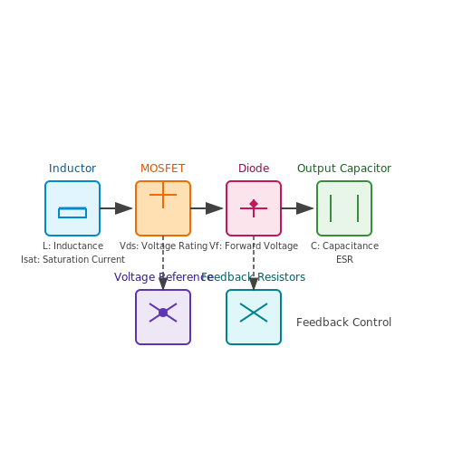
3. Energy Transfer Mechanism
3.1 Energy Transfer Mechanism
The operation of a DC-DC boost converter centers around the transformation of electrical energy from a lower voltage to a higher voltage. Understanding this energy transfer mechanism is crucial for designing efficient power supplies and optimizing various applications such as battery-powered devices, renewable energy systems, and electric vehicles. At the heart of the boost converter is the inductor, which plays a pivotal role in energy storage and transfer. When the switch within the boost converter is closed, current begins to flow through the inductor, causing it to store energy in its magnetic field. This relationship can be represented by the well-known inductor voltage equation:- Switching Frequency: Higher frequencies can lead to smaller inductors and capacitors, but at the cost of increased switching losses.
- Inductor Selection: The choice of inductor impacts both the transient response and the stability of the output voltage.
- Capacitance: The output capacitor must be sufficient to smooth out voltage ripples while maintaining stability.
- Load Conditions: Variations in load impedance can affect the overall performance and efficiency of the converter.
3.2 Control Strategies for Boost Converters
Boost converters have garnered significant attention in power electronics, especially due to their ability to efficiently step up low input voltages to higher output levels. The performance of a boost converter is largely influenced by the control strategy implemented. Control strategies are pivotal as they determine how the converter responds to various operational conditions, ensuring stability and efficiency in dynamic environments. To elucidate this, we will explore several prominent control methods used in boost converters, including Voltage Mode Control (VMC), Current Mode Control (CMC), and Hybrid Control. Each method has unique characteristics and applications, thereby influencing design choices in various engineering contexts.Voltage Mode Control (VMC)
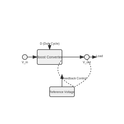
Voltage Mode Control is one of the traditional approaches employed in boost converters. The essence of VMC lies in regulating the output voltage by varying the duty cycle of the switch based on feedback from the output voltage. This technique is analyzed using a negative feedback configuration where the output voltage is compared to a reference voltage. In the VMC scheme, the error signal generated by this comparison is fed into a PWM (Pulse Width Modulation) modulator. This modulator adjusts the duty cycle of the switching element, aiming to minimize the error. The feedback loop ensures that the output voltage remains stable despite changes in load or input voltage. The advantages of VMC include simplicity and ease of implementation; however, it may be less responsive to fast transient loads compared to other methods.Current Mode Control (CMC)
Current Mode Control is another method that enhances the dynamic performance of boost converters. Unlike VMC, CMC utilizes an additional control loop that measures inductor current. This dual-loop control defines the output voltage while limiting the inductor current to prevent saturation. In practice, CMC operates as follows: the inductor current is sensed and compared against a current reference derived from the output Voltage. If the measured inductor current exceeds the reference, the duty cycle is curtailed to prevent excessive current flow. An intriguing aspect of CMC is that it naturally incorporates peak current limiting, which enhances system protection. Additionally, this strategy improves transient response. However, it also introduces complexity in design and potentially leads to suboptimal performance at very low duty cycles.Hybrid Control
The Hybrid Control strategy combines aspects of both VMC and CMC, leveraging their strengths and mitigating weaknesses. By employing both voltage and current feedback loops, Hybrid Control allows for robust output voltage regulation along with effective current limiting and improved transient response. This strategy utilizes a voltage loop for steady-state regulation and a current loop to address rapid changes in load. As a result, Hybrid Control is ideal for applications demanding high performance over a wide operating range, such as in renewable energy systems and battery management applications. In a typical implementation, the controller outputs to a PWM module that adjusts the switching signal based on both voltage and current demands, ensuring both stability and efficiency.Real-World Applications and Considerations
The choice of control strategy has significant implications in various applications. For instance: - VMC may be preferable in low-power applications where design simplicity is paramount. - CMC tends to be utilized in higher power systems where limiting peak currents is critical, such as in automotive power supplies or electric vehicle chargers. - Hybrid Control has gained traction in advanced applications where fast transient responses and stability under varying loads are required, such as in renewable energy systems or DC microgrids. In conclusion, understanding the nuances of each control strategy is essential for optimal design and performance of boost converters. As technology progresses towards more sophisticated demands, the exploration of advanced controls continues to evolve, inviting further research and innovation in the field of power electronics.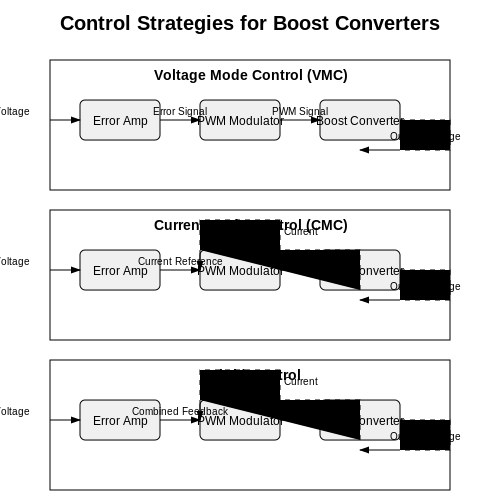
3.3 Feedback Loops in Operation
In the realm of DC-DC boost converters, feedback loops play a crucial role in regulating output voltage and ensuring stable operation across varying load conditions. The fundamental operation of a boost converter is predicated on its ability to elevate input voltage through a method of energy storage and release. Understanding feedback loops is pivotal as they directly influence the efficiency and reliability of power conversion in practical applications. Feedback in DC-DC converters generally refers to a control mechanism that adjusts the output based on sampled output voltage, thereby influencing the switching elements' duty cycle. The primary goal of this regulation technique is to maintain the output voltage at a desired set point despite fluctuations in load and input voltage.Control Techniques
Several control strategies can be employed in feedback loops, including voltage mode control, current mode control, and hysteretic control. Each of these methods has its pros and cons and suits various applications.- Voltage Mode Control: This technique regulates the output voltage by adjusting the duty cycle of the switching signal based on the difference between the output voltage and a reference voltage. This approach is simple and effective for many applications, but it can be slow to respond to load changes.
- Current Mode Control: In this strategy, the current flowing through the inductor is monitored and used in the control loop. This not only helps protect against overcurrent conditions but also enhances transient response and stability, as the converter can effectively respond to sudden load changes by regulating inductor current.
- Hysteretic Control: This method uses a comparison between the output voltage and set points to toggle the switching elements on and off. Its primary advantage lies in rapid response to load transients, making it ideal for systems requiring tight control and minimal voltage droop.
Implementing Feedback Loops
When implementing feedback loops in a boost converter circuitry, it is essential to account for various parameters such as gain, phase margin, and stability. The transfer function of the regulation loop, typically depicted in Bode plots, serves as a crucial tool for analyzing these factors. To go through the analysis of a simple voltage mode feedback system, we can start by defining the relationship between input and output voltages through a feedback loop in a transfer function form: 1. Model the output voltage as a function of the control variable (duty cycle) and the input voltage: $$ V_{out}(s) = G(s) \cdot V_{in}(s) \cdot D(s) $$ where \( G(s) \) is the transfer function of the boost converter. 2. Identify the output voltage feedback might be applied such that: $$ V_{ref} - V_{out}(s) $$ serves as the error signal fed into the controller. 3. Applying proportional control gives us: $$ D(s) = K_p \cdot (V_{ref} - V_{out}(s)) $$ where \( K_p \) is the proportional gain. This relationship highlights how deviations in output voltage from the reference value generate correction signals modifying the duty cycle, thereby adjusting the output to adhere to stability criteria. For real-world applications in embedded systems, feedback loops in boost converters contribute significantly to efficiency in battery management systems, automotive power supply, and renewable energy systems by minimizing voltage ripple and maximizing performance. The design can be further refined using advanced digital control techniques allowing programmable adjustment for varying outputs.Practical Considerations
When designing feedback loops for boost converters, engineers must also consider the impact of component selection—especially inductors, capacitors, and control ICs—on the overall system performance. Lower Equivalent Series Resistance (ESR) for capacitors, high-quality inductors with minimal core losses, and choosing the right control IC can drastically affect efficiency and thermal performance. In conclusion, a thorough understanding of feedback loops and their dynamic control techniques not only enhances the performance stability of DC-DC boost converters but also empowers engineers to tackle a variety of challenges in power electronics, leading to innovative solutions that drive technological advancement in energy management.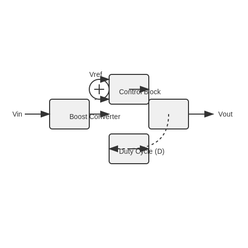
4. Efficiency Calculation
4.1 Efficiency Calculation
In the study of DC-DC boost converters, understanding the efficiency of the system is paramount due to its implications on thermal management, device longevity, and overall performance in practical applications. The efficiency of a boost converter can be defined as the ratio of the output power to the input power, typically expressed as a percentage. This section delves into the mathematical formulation and calculation of this efficiency, with particular attention to what factors influence it. The efficiency ($$\eta$$) can be mathematically expressed as: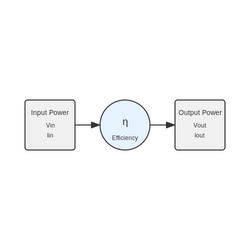
4.2 Factors Affecting Efficiency
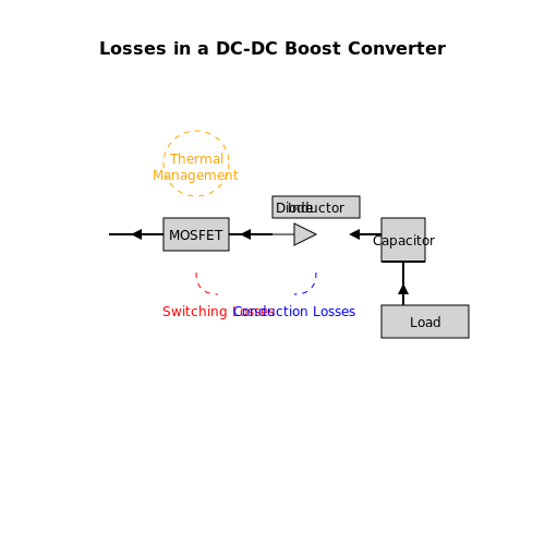
The efficiency of a DC-DC boost converter is a critical factor determining its performance and applicability across various sectors including renewable energy systems, electric vehicle technology, and portable electronic devices. Understanding the multitude of parameters that influence efficiency enables engineers and researchers to design more effective converters. Firstly, let us explore the inherent losses in a boost converter. Power losses can be categorized mainly into two types: conduction losses and switching losses. Conduction losses occur in the power switch (e.g., a MOSFET) and inductor during normal operation. The conduction loss in the switch can be expressed as:- Conduction and switching losses: Minimizing resistive losses in switches and inductors.
- Component choice: Utilizing high-quality inductors and low-ESR capacitors.
- Thermal management: Ensuring optimal operating temperatures for all components.
- Control strategies: Implementing intelligent feedback mechanisms to adjust to varying conditions.
4.3 Performance Characteristics
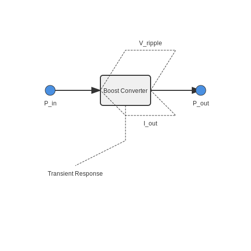
Understanding the performance characteristics of a DC-DC boost converter is essential for optimizing its design and ensuring efficient operation in practical applications. These characteristics can be influenced by several factors including circuit configuration, component selection, and operating conditions. In this section, we will explore key performance metrics such as efficiency, output voltage ripple, transient response, and thermal performance.
Efficiency
The efficiency of a boost converter is defined as the ratio of output power to input power and can be described mathematically as follows:
Where:
- η: Efficiency (in percent)
- Pout: Output power (in watts)
- Pin: Input power (in watts)
In practical scenarios, efficiencies can often exceed 90% under optimal conditions; however, losses occur due to factors such as conduction losses in switches, switching losses, and core losses in inductors. Continual advancements in semiconductor technology and circuit designs aim to improve efficiency in a wider range of operating conditions.
Output Voltage Ripple
Output voltage ripple is another critical performance metric, illustrating the variability of the output voltage relative to its desired value. This ripple is primarily caused by the charging and discharging of output capacitors and can be calculated using:
Where:
- Vripple: Peak-to-peak output voltage ripple (in volts)
- Iout: Load current (in amperes)
- f: Switching frequency (in hertz)
- Cout: Output capacitance (in farads)
Designers often prioritize minimizing ripple to improve load regulation and enhance the performance of downstream components.
Transient Response
The ability of a boost converter to handle sudden changes in load is crucial for applications where the power demand can fluctuate significantly (e.g., battery-operated devices). The transient response is characterized by the time it takes for the output voltage to settle to the desired level following a disturbance. Key factors affecting transient response include:
- Type and value of the output capacitor
- Control loop design
- Inductor size and saturation characteristics
A well-designed control loop can significantly enhance transient performance by enabling more rapid adjustments to the duty cycle, thus allowing the converter to respond quickly to changes in load demand.
Thermal Performance
Thermal management is paramount in DC-DC boost converters, as excessive heat can degrade performance and reliability. Heat generation primarily stems from:
- Switching losses during rapid transitions
- Conduction losses through resistive components (e.g., MOSFETs and inductors)
To optimize thermal performance, components should be chosen based on their thermal ratings and should be arranged to facilitate adequate heat dissipation. Advanced designs may incorporate heatsinks, thermal pads, or active cooling systems to maintain optimal operating temperatures.
In conclusion, a thorough understanding of the performance characteristics of DC-DC boost converters is essential for engineers and researchers looking to design efficient, robust power supply systems for various applications. By considering efficiency, output voltage ripple, transient response, and thermal management, one can significantly enhance the efficacy of these converters in real-world conditions.
5. Portable Devices and Battery Charging
5.1 Portable Devices and Battery Charging
DC-DC boost converters are essential components in the realm of portable devices and battery charging applications, enabling efficient power management by stepping up low input voltages to higher output voltages. This capability is critical in scenarios where battery voltages fall below the operational thresholds required by certain electronic circuits. Understanding the operational mechanism and application scenarios of boost converters can greatly enhance the performance and efficiency of portable electronics.
The boost converter operates on a fundamental principle of energy storage and release. By utilizing an inductor, switch (typically a MOSFET), diode, and capacitor, the converter can transfer energy from the power source to the load. The heart of the boost converter lies in its ability to operate in a switch-mode, whereby it alternates between two states: charging the inductor and discharging it to the output. This operation can be succinctly described by analyzing the inductor voltage during the two phases of the switching cycle.
Basic Operation and Efficiency Considerations
During the 'ON' phase, when the switch is closed, the inductor charges up, and the voltage across it increases according to the equation:
Here, \( V_L \) represents the voltage across the inductor, \( L \) is the inductor's inductance, and \( \frac{di}{dt} \) is the rate of change of current. When the switch turns 'OFF', the inductor current continues to flow, but now its energy is transferred to the output capacitor and load, causing the output voltage to increase:
In this equation, \( V_{out} \) is the output voltage, \( V_{in} \) is the input voltage, and \( D \) is the duty cycle of the converter. As \( D \) approaches 1, the output voltage can significantly exceed the input voltage. However, the efficiency of this energy conversion remains a critical focus, particularly for battery-powered applications. Losses due to inductor resistance, switch losses, and diode conduction losses can lead to inefficiencies that degrade battery life and performance.
Applications in Portable Devices
Boost converters find versatile applications in portable devices, enhancing functionality while maintaining compact size. Common applications include:
- Smartphones and Tablets: These devices often use boost converters to power higher voltage components, optimizing battery discharge and extending operational time between charges.
- Wearable Technology: In wearables, where space is at a premium, boost converters allow for the use of smaller batteries while providing sufficient voltage to various sensors and displays.
- LED Drivers: Boost converters are extensively employed for driving LEDs in handheld devices, ensuring consistent brightness and performance even when battery levels fluctuate.
One significant advantage of integrating a boost converter in these applications is the management of varying load conditions. Advanced controllers can dynamically adjust the duty cycle, enhancing efficiency based on real-time demands, thus conserving battery life.
Battery Charging Implementation
A prominent application of boost converters is in battery charging systems, especially for lithium-ion and lithium-polymer batteries. These batteries require specific charging profiles, often needing higher voltage levels than the battery's current state to charge efficiently. A boost converter enables compatibility with lower voltage sources, such as USB ports or solar panels, facilitating effective charging under variable conditions.
The charging circuit design may incorporate feedback mechanisms for maintaining a regulated output voltage, preventing overcharging and ensuring battery longevity. This adjustment is vital, as different battery chemistries possess varied voltage thresholds and current requirements, emphasizing the versatility of boost converters in modern energy solutions.
As we continue exploring the interplay between DC-DC converters, energy management, and battery technology, the advancements in materials and circuit design promise to yield even greater efficiencies and capabilities in future portable and battery-operated devices.
5.2 Power Supply for LED Drivers
As the demand for energy-efficient lighting solutions continues to rise, LED (Light Emitting Diode) technology has emerged as a leading choice due to its low power consumption and long lifespan. However, effectively driving LEDs requires a reliable and efficient power supply, often achieved through the use of DC-DC boost converters.
LEDs generally operate at a low forward voltage; hence, when the supply voltage is insufficient to drive the LED load, a boost converter becomes essential. This converter takes a lower input voltage and steps it up to a higher output voltage, allowing the LED to function optimally. The basic operation revolves around the principles of electromagnetic induction and energy conservation, crucial for understanding how these circuits function.
The Role of DC-DC Boost Converters in LED Operation
The core purpose of a boost converter in LED applications is to maintain a constant output voltage while ensuring fluctuating input sources can still power the LEDs accurately. The boost converter operates by using an inductor, a switch (typically a transistor), a diode, and a capacitor. When the switch is closed, current flows through the inductor, storing energy in its magnetic field. On opening the switch, the energy stored is released to the output, increasing the voltage.
To analyze the operational efficacy of a boost converter, we can derive the voltage and current relationships within the system. Assuming an ideal inductor and neglecting losses, the output voltage \( V_{out} \) can be defined as:
where:
- Vin is the input voltage.
- D is the duty cycle (the fraction of time the switch is on during each switching cycle).
This equation exemplifies how adjusting the duty cycle allows the converter to control the output voltage to meet the LED requirements effectively.
Efficient Optimization Techniques
To achieve maximum efficiency, which is crucial for low-power applications like LED drivers, several strategies can be employed:
- Switching Frequency Optimization: Selecting an appropriate switching frequency ensures efficient energy transfer while minimizing losses.
- Controlled Duty Cycle: Modulating the duty cycle dynamically based on load conditions can help achieve desired performance with minimal energy waste.
- Inductor Selection: The selection of a suitable inductor value can significantly impact the ripple current and overall efficiency of the converter.
Moreover, controlling the output with feedback mechanisms can maintain precision in LED brightness, ensuring consistent performance throughout operation.
Practical Applications in the Industry
DC-DC boost converters are widely utilized in various lighting applications, ranging from simple household LED bulbs to intricate LED displays and automotive lighting systems. In such cases, the converter design must account for environmental factors, component tolerances, and operational longevity to enhance user experience and product efficiency.
With advancements in semiconductor technology, many integrated circuits now offer built-in boost converter functions, simplifying design and increasing reliability. These advancements allow for smaller, more efficient, and more cost-effective solutions tailored to consumer needs.
Overall, understanding the synergy between DC-DC boost converters and LED drivers invites further exploration into enhancing power management systems within modern electronics.
5.3 Renewable Energy Systems
Incorporating DC-DC boost converters into renewable energy systems has become increasingly essential due to the variable output conditions inherent in sources like solar and wind energy. The ability to efficiently convert low-voltage outputs from these sources to higher voltage levels makes boost converters a critical component in achieving maximum energy utilization.
At their core, boost converters enable energy storage systems, such as batteries and supercapacitors, to operate effectively by stepping up the voltage, thereby allowing seamless integration with various load requirements. This section delves deeper into the operational principles, advantages, integration examples, and real-world implications of DC-DC boost converters within renewable energy systems.
Understanding the Operational Mechanism
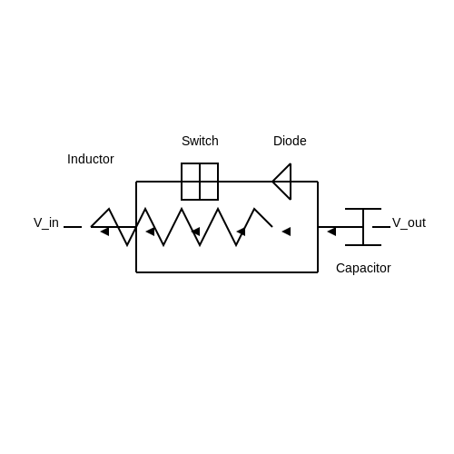
A boost converter operates on the principle of storing energy in an inductor and then releasing it to the output at a higher voltage. The fundamental components of a boost converter include:
- Inductor: Stores energy when a switch (transistor) is closed.
- Switch: Usually a transistor that opens and closes to control the inductor's charge and discharge cycle.
- Diode: Prevents current from flowing back into the inductor.
- Capacitor: Smooths the output voltage after the energy has been released.
During operation, when the switch is closed, current flows through the inductor, and energy is stored. When the switch opens, the inductor's magnetic field collapses, and the energy is released into the output capacitor, increasing the output voltage.
In this equation, Vout is the output voltage, Vin is the input voltage, and D is the duty cycle. This relationship highlights that as the duty cycle increases, so does the output voltage, making the boost converter particularly useful in renewable energy scenarios where voltage levels may fluctuate.
Advantages of Using Boost Converters in Renewable Energy
The integration of boost converters in renewable energy systems presents numerous advantages:
- Increased Efficiency: Boost converters enhance the overall energy efficiency by converting lower voltage outputs into higher voltages suitable for consumption.
- Improved Output Stability: They can handle sudden changes in load demand and help maintain a stable output voltage.
- Flexibility: The design allows for adaptation to various renewable energy sources and storage solutions.
Case Studies and Real-World Applications
Several applications illustrate the relevance of DC-DC boost converters in renewable energy systems:
- Solar Power Systems: In off-grid solar applications, low voltage from solar panels is boosted to charge batteries or feed into the grid while meeting local voltage requirements.
- Wind Turbine Power Generation: Boost converters play a critical role in maximizing the output power from variable-speed wind turbines by regulating and adapting the voltage efficiently.
- Electric Vehicles (EVs): Many EV charging stations utilize boost converters to step up the voltage from renewable sources, thereby improving charging times and efficiency.
Overall, the principles governing the operation of boost converters directly contribute to enhanced renewable energy systems that are resilient, efficient, and capable of meeting modern energy demands.
Conclusion
In summary, the role of DC-DC boost converters in renewable energy systems cannot be overstated. Their ability to efficiently up-convert voltages plays a pivotal role in maximizing the utilization of renewable energy sources, thus promoting sustainable energy solutions crucial for the energy transition.
6. Common Issues in Boost Converter Circuits
6.1 Common Issues in Boost Converter Circuits
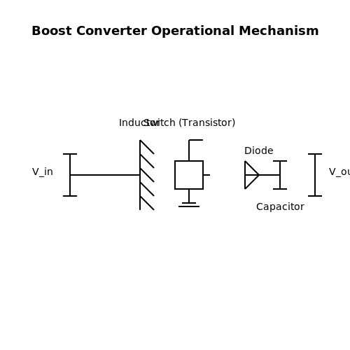
DC-DC boost converters, while essential for stepping up voltage levels in various electronic applications, can encounter a range of common issues that affect their performance and reliability. Understanding these challenges is crucial for engineers and researchers when designing and implementing these circuits.
Voltage Ripple and Output Noise
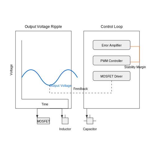
One of the primary concerns in boost converter circuits is the voltage ripple at the output. Voltage ripple arises from the charging and discharging cycles of the output capacitor, which can lead to unstable voltage levels. This effect is exacerbated by the switching frequency and the inductor current ripple.
To mitigate output ripple, designers can employ larger output capacitors or ceramic capacitors with low equivalent series resistance (ESR). Additionally, filtering techniques, such as LC filters, can further smooth out the output voltage.
Efficiency Losses
Efficiency is critical in power conversion, as it directly impacts thermal management and battery life in portable applications. Various factors contribute to efficiency losses in boost converters, including:
- Conduction losses: Caused by the resistance in circuit components, such as MOSFETs and inductors.
- Switching losses: Occur when the switches turn on and off, resulting in power dissipation during transitions.
- Core losses: Associated with the magnetic materials in inductors and transformers due to hysteresis and eddy currents.
Designers can optimize efficiency by selecting components with lower RDS(on) for MOSFETs, minimizing the switching frequency to reduce losses, and employing proper thermal management techniques.
Control Loop Stability
The control loop in a boost converter is vital for maintaining desired output voltage and responding to load variations. However, instability can arise due to inadequate phase margin or improper compensation design. This can result in oscillations, suboptimal transient response, and even system failure.
To enhance stability, engineers often apply control techniques such as voltage mode control, current mode control, or PID (Proportional-Integral-Derivative) control, which can significantly improve transient response and system robustness. Simulating the control loop using Bode plot analysis can also provide insights into stability margins.
EMI Issues
Conducted and radiated electromagnetic interference (EMI) is a crucial consideration in DC-DC converter applications, especially in sensitive environments such as avionics or medical devices. The fast switching transitions and high di/dt in boost converters can create significant EMI challenges.
To minimize EMI, designers can utilize techniques such as:
- Snubber circuits: To dampen voltage spikes.
- Proper layout design: Including ground planes and minimizing loop areas to reduce inductance.
- Shielding: Encasing sensitive circuits to mitigate radiated emissions.
In summary, while boost converters are indispensable in modern electronics, they present several engineering challenges that require careful consideration and solution approaches. Addressing these common issues—such as ripple voltage, efficiency losses, control loop stability, and EMI—can significantly enhance the performance and reliability of these power conversion systems.
6.2 Design Best Practices
In the intricate arena of DC-DC boost converters, adhering to a set of design best practices often distinguishes proficient engineers from their less experienced counterparts. The effectiveness of these converters—coupled with their prominence in applications that require efficient voltage step-up solutions, such as battery-operated devices and renewable energy systems—demands rigorous attention to detail in their design phase.Understanding the Operating Principles
Before delving into design practices, it's crucial to recognize the fundamental operating principles of a boost converter. Unlike linear regulators, boost converters provide a higher output voltage from a lower input voltage by storing energy in an inductor and releasing it when needed, governed by a switching element. This mechanism not only improves efficiency but also minimizes heat dissipation, making them ideal for low-power electronic applications.Essential Design Considerations
The design of a boost converter can be influenced by numerous factors. Here are several critical considerations for optimizing both performance and reliability:1. Inductor Selection
The inductor plays a vital role in energy storage and output voltage ripple management. When selecting an inductor, the following parameters should be evaluated:- Inductance Value: Proper inductance must be chosen to achieve the desired output voltage and current. The inductance can be calculated using the formula:
$$ L = \frac{(V_{out} - V_{in}) \cdot D}{\Delta I_L \cdot f_{sw}} $$where:
- $$V_{out}$$ — Desired output voltage
- $$V_{in}$$ — Input voltage
- $$D$$ — Duty cycle
- $$\Delta I_L$$ — Allowable inductor ripple current
- $$f_{sw}$$ — Switching frequency
- Current Rating: Ensure the selected inductor can handle the maximum current without saturating. Over-saturation can lead to inefficiencies and reliability issues.
2. Output Capacitor Selection
The output capacitor significantly influences output voltage ripple and transient response. Key factors to consider include:- Capacitance: Larger capacitance values help reduce voltage ripple, while too high values may introduce stability issues.
- Equivalent Series Resistance (ESR): A low ESR improves efficiency and stability.
3. Component Placement and Layout
A robust layout is pivotal for minimizing electromagnetic interference (EMI) and optimizing thermal management:- High-Frequency Paths: Keep switching nodes (in/out of the switch and diode) as short as possible to minimize loop area.
- Thermal Management: Ensure adequate heat sinking and spacing between heat-generating components to maintain operational integrity.
4. Feedback Control Loop Design
The feedback control loop is critical for maintaining output voltage stability under varying load conditions. Here are principles to guide the design:- Compensation Techniques: Employ methods like voltage-mode or current-mode control to ensure robust transient response.
- Bode Plot Analysis: Use Bode plots to analyze the stability of the system by ensuring that gain and phase margins are adequate.
Real-World Applications
Understanding and implementing these design best practices can translate directly into enhanced efficacy and reliability of boost converters in various applications. For instance, in solar power systems, the ability to efficiently step up low voltages is essential for maximizing power extraction and minimizing losses. Likewise, in portable electronics, where battery life is a critical design consideration, applying these principles ensures sustained performance across the operational spectrum. In summary, the design of DC-DC boost converters is a complex but rewarding endeavor that necessitates careful consideration of component selection, layout strategies, and control mechanisms. By embracing these best practices, engineers can contribute to the development of efficacious and dependable power management systems that meet the demands of modern technology.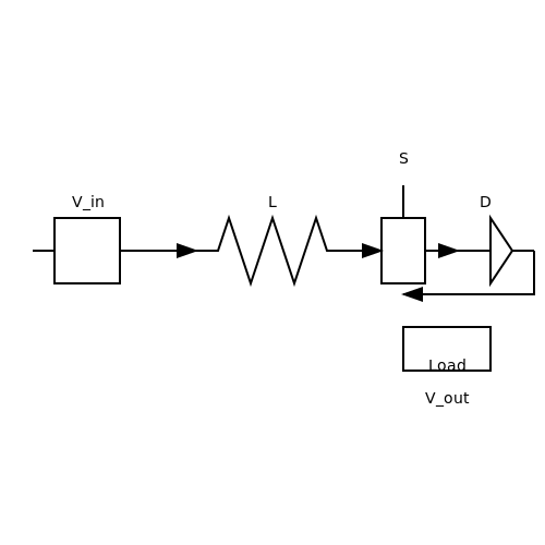
6.3 Simulation Tools for Circuit Analysis
The efficacy of a DC-DC boost converter depends not only on its design but also on the precise understanding of electrical behaviors which can be notoriously complex. To demystify these phenomena, simulation tools play an invaluable role in circuit analysis by providing engineers, physicists, and researchers with platforms to visualize and test their designs before physical implementation. This subsection delves into various simulation tools tailored for analyzing DC-DC boost converters, equipped with functionality suitable for advanced users.
Simulation environments utilize mathematical models to replicate circuit behaviors under a variety of conditions. By adjusting parameters such as load resistance, input voltage, and switching frequency, users can gain insights into efficiency, ripple voltages, and transient responses. Notably, these tools enable comprehensive analyses that can predict performance issues — aspects crucial for designing reliable power electronics.
Key Simulation Tools and Their Features
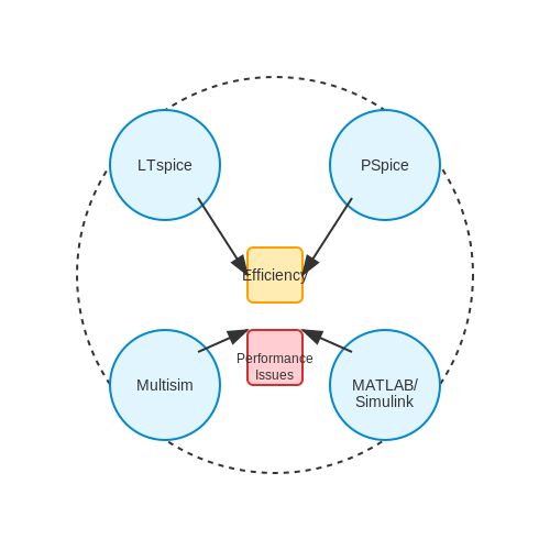
In the world of electronics, several well-regarded simulation tools can facilitate circuit analysis for DC-DC converters. Each tool offers distinct capabilities, allowing practitioners to choose one suited to their specific project requirements:
- LTspice: A free SPICE-based simulator widely utilized for circuit simulation. It provides an efficient means to model and analyze DC-DC converters, allowing users to simulate parameter sweeps and transient responses in great detail.
- PSpice: This advanced version of SPICE includes support for both analog and digital circuitry. PSpice allows the simulation of complex DC-DC configurations, enabling the validation of design assumptions and efficiency optimizations.
- MATLAB/Simulink: Well-known in the engineering community, MATLAB's Simulink offers powerful simulation capabilities through block diagrams, enabling real-time modeling of dynamic systems which can be crucial for boost converter analysis under varying load conditions.
- Multisim: Developed by National Instruments, Multisim integrates circuit simulation with a robust graphical interface. Engineers can simulate DC-DC converters with both theoretical and experimental approaches, leveraging built-in components and functionality for ease of use.
Advantages of Circuit Simulation
Utilizing these simulation tools presents several advantages:
- Cost-Effectiveness: Simulation reduces the necessity for costly prototyping, enabling early detection of potential issues.
- Time Efficiency: Engineers can iterate designs quickly without the delays associated with physical adjustments.
- Comprehensive Analysis: Different operating conditions can be simulated to understand the converter's behavior across a range of scenarios, paving the way for robust design solutions.
For instance, if one were to simulate power losses in a boost converter under varying input voltages, tools like PSpice could seamlessly calculate the grounding inductance and output capacitance, helping to optimize performance.
Conclusion and Practical Applications
Inversely, the reliance on simulation tools is not merely an academic exercise; their utility transgresses into real-world applications. Industries such as electric vehicles, renewable energy systems, and consumer electronics leverage simulation results to manufacture efficient and reliable DC-DC converters. Understanding how to effectively utilize these tools is paramount for engineers who aim to push the boundaries of power electronic design further into innovation.
7. Emerging Technologies
7.1 Emerging Technologies
DC-DC boost converters have evolved significantly, driven by advancements in materials science, integration techniques, and control algorithms. As power systems demand higher efficiency and flexibility, emerging technologies promise to reshape the landscape of DC-DC conversion.
Wide Bandgap Semiconductors
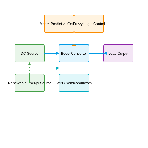
One of the most revolutionary advancements in boost converter technology is the adoption of wide bandgap (WBG) semiconductors, such as silicon carbide (SiC) and gallium nitride (GaN). These materials possess superior thermal conductivity and breakdown field strength compared to traditional silicon, enabling converters that operate at higher frequencies and temperatures.
By leveraging WBG semiconductors, designers can reduce the size of magnetic components due to diminished energy storage requirements, enhancing the overall power density. The increase in switching frequency also leads to lower ripple voltages, which improves overall efficiency. Case studies have shown that converters utilizing GaN can achieve efficiencies exceeding 98% under specific load conditions.
Integrated Circuit Designs
Recent trends also emphasize integrating various converter components into single-chip solutions. These power integrated circuits (PICs) combine control, driver, and switching functions, reducing the overall footprint and simplifying circuit design. Integrated converter solutions are particularly beneficial in applications where space is limited, such as in portable devices and electric vehicles.
The integration facilitates optimized communication among components, improving performance metrics like transient response and reduced electromagnetic interference (EMI). As more manufacturers pursue these designs, the availability of integrated solutions helps drive costs down and enhance reliability.
Advanced Control Techniques
In tandem with hardware advancements, control strategies for boost converters have also seen remarkable innovation. Techniques such as model predictive control (MPC) and fuzzy logic control (FLC) enable converters to dynamically adjust to varying load conditions, thereby optimizing efficiency dynamically. These control methods can adapt to changing input voltage and load current instantly, maintaining a stable output under various conditions.
Moreover, the implementation of digital control systems offers enhanced flexibility in adjusting parameters post-deployment, allowing converters to be fine-tuned for specific applications without requiring physical alteration.
Applications in Renewable Energy
As global energy demands shift towards sustainability, DC-DC boost converters are finding critical applications in renewable energy systems. For instance, in solar energy systems, boost converters are employed to increase the output voltage from solar panels, making it compatible with inverter inputs. The increased efficiency from emerging technologies in this sector leads to significant gains in power conversion, directly affecting overall system performance and sustainability.
In electric vehicles (EVs), advanced boost converters play an essential role in battery management systems, ensuring maximized energy utilization and improving vehicle range. The shift towards integrated solutions and WBG semiconductors further enhances the viability and attractiveness of advanced DC-DC converters in EV applications.
In conclusion, the landscape of DC-DC boost converters is rapidly evolving with the advent of new materials, integrated designs, and advanced control methodologies. This progression signifies not merely technological advancement but also a substantial impact on future applications across various domains, paving the way for more efficient and compact power systems.
7.2 Integration with Smart Systems
As the world edges closer to greater automation and intelligent systems, the role of power electronics becomes increasingly pivotal. Among these electronics, the DC-DC boost converter stands out, not only as a piece of hardware that harnesses electrical energy efficiency but also as a critical component that enables smart systems to function optimally. It allows various low-voltage devices to operate efficiently, providing them with the necessary higher voltage levels without sacrificing battery life or energy efficiency.
Smart systems, including those used in Internet of Things (IoT) devices, electric vehicles, and renewable energy systems, depend heavily on reliable and adaptable power supplies. In this context, the integration of boost converters allows these systems to operate in variable conditions, supporting a range of applications that require power management. For instance, in battery-powered IoT devices, a boost converter may be used to step up the voltage provided by batteries, ensuring consistent function even as the battery discharges.
Efficiency and Control Schemes
The efficiency of a boost converter is a crucial factor for its integration into smart systems. With the evolving demands on power systems, it becomes essential to utilize advanced control schemes to enhance the performance of boost converters. Techniques such as voltage regulation and current control enable the converter to adapt to varying load conditions, ensuring that the system maintains a stable output voltage.
A common method employed is feedback control, where the output voltage is continually monitored and compared to a reference voltage. This loop allows adjustments to the switching duty cycle in real-time, improving response times and stabilizing the power output. The equations governing the duty cycle \(D\) for an ideal boost converter help illustrate this principle:
By manipulating the duty cycle, the system can dynamically alter output voltage levels, making the boost converter an essential component for meeting the fluctuating power demands in smart applications.
Case Studies: Applications in Smart Systems
In practical terms, several case studies exemplify the integration of DC-DC boost converters in smart systems:
- IoT Sensor Networks: These often operate in low-power conditions and rely on boost converters to ensure consistent performance across varying supply voltages.
- Electric Vehicles: In hybrid and electric vehicles, boost converters are used to manage energy conversion from batteries to motors, ensuring efficiency during acceleration and energy recovery during braking.
- Solar Energy Systems: Here, boost converters enhance the output from photovoltaic cells, allowing for better energy harvest and storage in batteries, facilitating optimal energy usage.
In each of these examples, the boost converter not only enhances voltage levels but also interacts with other system components, ensuring that energy supply is both efficient and reliable.
Future Directions
As technology matures, further integration of smart functionalities into DC-DC boost converters can be expected. Innovations such as digital control loops, adaptive voltage scaling features, and integration with data logging systems for predictive maintenance are on the horizon. These advancements will streamline operations and promote longer-lasting devices, all while maximizing energy efficiency.
In conclusion, the role of the DC-DC boost converter in smart systems cannot be overstated. Its ability to enable efficient power management underpins numerous applications, driving forward the development and effectiveness of modern electronic devices.
7.3 Environmental Considerations
In the design and implementation of DC-DC boost converters, environmental considerations play a crucial role in ensuring both efficiency and sustainability. As electronic devices become increasingly ubiquitous, their environmental impact throughout their life cycle, including production, operation, and disposal, becomes ever more significant. One primary concern is the material selection used in the construction of boost converters. With an emphasis on reducing ecological footprints, engineers are increasingly opting for materials that are both high-performing and have a minimal environmental impact. For example, the transition to using lead-free solder and halogen-free components has become a standard practice. These materials not only align with regulatory requirements but also mitigate the release of toxic substances during manufacturing and disposal. Another critical aspect to consider is energy efficiency. The main function of a boost converter is to step up voltage from a lower level to a higher one, but this process can often incur energy losses. The efficiency of the boost converter is commonly determined by its input and output voltages, the load conditions, and the components used (inductors, capacitors, and switching devices). Maximizing efficiency not only helps in reducing the environmental footprint during operation but also contributes to prolonging the lifespan of the electronic devices they power. The efficiency \( \eta \) of a boost converter can be expressed as:8. Key Texts on Power Electronics
8.1 Key Texts on Power Electronics
- Power Electronics: Devices, Circuits, and Applications — This book provides comprehensive coverage on various power electronics topics, offering deep insights into power device operation and circuit topologies.
- Power Electronics Handbook by Muhammad Rashid — This handbook is an all-inclusive resource on power electronics, illustrating the principles and techniques involved in the design and implementation of power electronic systems.
- Power Electronics and Motor Drives: Advances and Trends — Focuses on recent advances in power electronics and drives, highlighting innovations pertinent to electric traction and automotive applications.
- Principles of Power Electronics by John Kassakian — A foundational text that covers various strategies and practical techniques for power electronics and their cross-disciplinary applications.
- Advanced Power Electronics Converters by Ebrahim Babaei — Provides an overview of current research directions and technologies in the field of power electronics, aiming to guide future development.
- Fundamentals of Power Electronics by Robert Erickson — Offers a deep dive into the principles of operation, design, and regulation of power electronic circuits, complete with mathematical models.
- Power Electronics: A First Course by Ned Mohan — A practical and introductory guide to power electronics fundamentals, ideal for those new to the field.
8.2 Research Papers and Journals
- DC–DC Boost Converter Design Methodology — This research paper provides a thorough examination of design methodologies for DC-DC boost converters. It includes various simulation outputs to corroborate its findings and discusses the converter's efficiency metrics.
- Dynamic Analysis of Boost Converters — Published in the IEEE Transactions on Power Electronics, this paper delves into the dynamic behaviors of boost converters under varied load conditions, offering a systematic approach to stability analysis.
- Advancements in DC-DC Power Converter Technologies — A comprehensive survey that discusses recent advancements in DC-DC power converters, with a strong focus on innovations enhancing the performance and efficiency of boost converters.
- Analysis of Boost Converters for Renewable Energy Applications — This journal article assesses the applicability of boost converters in renewable energy systems, especially with solar panels, while providing insights on optimizing converter designs for solar arrays.
- Performance Evaluation of Different Boost Converter Variants — A detailed evaluation of various types of boost converters employed in industrial settings, focusing on performance factors such as efficiency and thermal management.
- High-Efficiency DC-DC Converters for Energy Storage Applications — This paper explores the design and real-world implementation of high-efficiency DC-DC converters, ideal for energy storage applications, enhancing voltage regulation and prolonging battery life.
- Techniques for Reducing Ripple in Boost Converters — Focused on the reduction of voltage and current ripple issues commonly found in boost converters, this technical paper investigates several filtering and modulation strategies.
8.3 Online Resources and Tutorials
- Arrow DC-DC Boost Converter Tutorial — A comprehensive guide covering the theory, design principles, and practical applications of DC-DC boost converters. Suitable for advanced learners, this resource includes detailed explanations and circuit design tips.
- Electronics Tutorials - Boost Converter — Provides an in-depth look at the operation and characteristics of boost converters, including mathematical descriptions and practical usage scenarios for engineers.
- Texas Instruments: Understanding Boost Power Stages — A technical application note that addresses the design and operation of boost power stages, replete with rigorous mathematical derivations and laboratory results.
- Analog Devices: Boost Power Stages in Switching Power Supplies — This article delivers complex technical details on switching power supplies, focusing on boost stage operations with high-level design considerations.
- YouTube - Detailed Boost Converter Analysis — A video resource that breaks down the principles of DC-DC boost converters using real-world examples and simulations. It is especially useful for visual learners who want to strengthen their conceptual understanding.
- Digi-Key: Implement Boost Converters for Battery Applications — Offers a specialized perspective on incorporating boost converters into battery-operated devices, with an emphasis on efficiency and practical implementation strategies.
- EDN Network: Designing a Boost Converter from Scratch — This resource provides a step-by-step guide to building a boost converter, complete with circuit analysis, component selection, and troubleshooting advice for advanced users.
- EE Times: Design Considerations for DC-DC Booster Converters — Discusses high-level design considerations, including frequency management and thermal performance, crucial for sophisticated DC-DC boost converter applications.