12V to 5V Buck Converter DIY
1. What is a Buck Converter?
1.1 What is a Buck Converter?
A buck converter is a type of DC-DC converter that efficiently steps down voltage from a higher level to a lower level while maintaining power supply efficiency. This regulator is essential for numerous applications in modern electronics, ranging from power supplies for microcontrollers to automotive systems, owing to its ability to provide stable outputs even under variable load conditions.
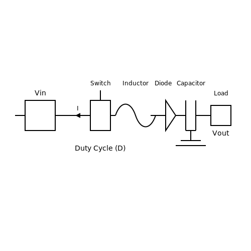
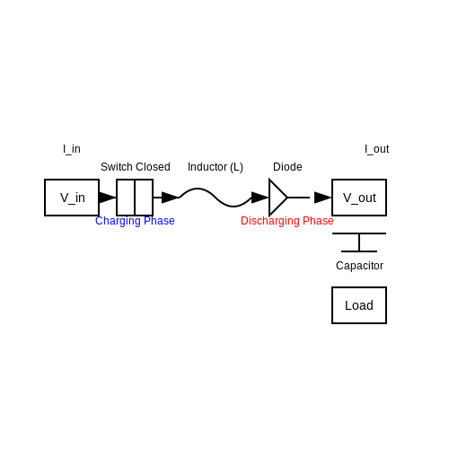
At its core, a buck converter operates on the principle of inductor energy storage. During the on-state cycle, a switch (often a transistor) allows current to flow through an inductor. As current builds, energy is stored in the magnetic field of the inductor. When the switch turns off, the inductor releases its stored energy to the output through a diode. This process leads to a voltage reduction at the output relative to the input voltage.
Operational Principles
The operational principles of a buck converter can be better understood with respect to its fundamental components:
- Switch (Transistor): This component rapidly opens and closes, controlling the current flow into the inductor. It is usually driven by a PWM (Pulse Width Modulation) signal, which determines the percentage of time the switch remains closed, thereby regulating the output voltage.
- Inductor: This energy storage component allows the converter to maintain a continuous output current. Its reactance changes dynamically with the current flowing through it, which is pivotal during the switch's on and off phases.
- Diode: The role of the diode is to permit current flow during the off cycle of the switch, ensuring that the inductor’s energy is delivered to the load effectively.
- Circuit Capacitors: These components help smooth out the output voltage, reducing ripples and providing a stable voltage to the load.
The relationship between these components can be mathematically derived. The output voltage \( V_{out} \) of a buck converter can be expressed with respect to the input voltage \( V_{in} \) and the duty cycle \( D \) (the ratio of the time the switch is on to the total cycle time). The basic relationship is given by:
Where \( D \) is typically between 0 and 1, translating to output voltages that can range from 0 to a value nearly equivalent to \( V_{in} \). This linear relationship indicates how adjusting the duty cycle directly modifies the output voltage, showcasing the converter's flexibility.
Efficiency Considerations
One of the defining advantages of using buck converters lies in their efficiency. Buck converters typically reach efficiencies of 90% or higher due to their ability to minimize energy losses compared to linear voltage regulators, which dissipate excess voltage as heat. This efficiency is paramount in battery-powered applications where conserving energy prolongs operational life.
As such, buck converters are not only versatile and powerful but also essential for developing compact, energy-efficient designs in various electronic applications including computing, automotive electronics, and renewable energy systems.
1.2 Applications of Buck Converters
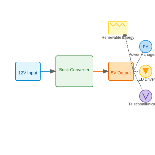
Buck converters, also known as step-down converters, have become essential components in modern electronics due to their efficiency and versatility in voltage regulation. These devices are primarily used to convert a higher input voltage to a lower output voltage while maintaining high efficiency, often exceeding 90%. The practical relevance of these converters spans various fields and applications, reflecting their importance in both consumer electronics and industrial settings.
Power Management Systems
One of the most significant applications of buck converters is in power management systems. In scenarios where multiple voltage levels are required, such as in smartphones or tablets, buck converters provide an efficient means of digitizing power supply. They can take a common voltage source, say 12V, and deliver the required 5V or 3.3V for logic circuits and sensors without significant energy loss. This aspect is critical for extending battery life and optimizing performance in portable devices.
Renewable Energy Systems
In renewable energy systems, buck converters play a pivotal role in solar energy applications. Photovoltaic systems often require efficient DC-DC converters to manage the varying output voltages produced by solar panels, which can fluctuate based on light conditions. Here, a buck converter can stabilize the output voltage delivered to the battery storage system, ensuring compatibility, enhancing charging efficiency, and prolonging the lifespan of storage batteries.
LED Driver Applications
Another application lies in driving LED arrays. LEDs require a constant current for optimal performance, and since many power sources exceed the required forward voltage, a buck converter is used to step down the voltage and regulate the current accordingly. This capability ensures reliability and longevity of the LED components, particularly in high-power applications like automotive lighting and architectural illumination.
Telecommunications
In the telecommunications sector, buck converters facilitate voltage regulation within communication devices, which typically require multiple voltage levels for different circuits. For example, base stations and routers utilize buck converters to provide various supply voltages necessary for processors, RF amplifiers, and other components. This functionality is vital for maintaining signal integrity and minimizing power consumption within the network.
Microcontroller Power Supplies
Microcontrollers often operate at lower voltages (usually 3.3V or 5V) but may require higher input voltages for specific functionalities. Buck converters enable the conversion from a higher voltage source to the needed voltage efficiently, thus enhancing the overall performance and reliability of embedded systems. This conversion allows engineers to optimize battery-operated devices to draw power effectively while minimizing wasted energy.
Automotive Applications
In automotive applications, buck converters have gained traction due to the need for efficient power distribution among various electrical components. Many devices within vehicles, including audio systems, navigation devices, and onboard computers, benefit from the compact size and high efficiency of buck converters. Their ability to handle wide input voltage ranges further ensures compatibility with automotive power systems, which may see variations due to engine load and other factors.
As engineering evolves, the applications of buck converters will likely expand, driven by the demands for efficiency, miniaturization, and versatility in all sectors of technology. Their integration into new designs will continue to support the global movement towards greener, more efficient energy solutions and complex electronic systems.
1.3 Working Principle of Buck Converters
A buck converter is a fundamental component in modern electronics, used extensively for voltage regulation in various applications, including power supplies, battery chargers, and electric vehicles. The principle behind a buck converter is deceptively simple yet grounded in the laws of electromagnetic induction and circuit theory.
The primary function of a buck converter is to step down a higher input voltage to a lower output voltage efficiently. This process involves energy transfer between an inductor and a capacitor, governed by the switching operation of a transistor. Let's delve deeper into the key components and their roles in this dynamic energy conversion process.
Basic Components of a Buck Converter
At the core of a buck converter, several crucial elements work in tandem:
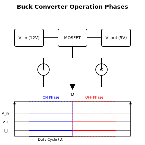
- Switching Element (Transistor): This is typically a MOSFET that rapidly toggles between its ON and OFF states to control current flow.
- Inductor: Stores energy when the switching element is ON and releases it when the switch is OFF, providing a continuous current to the load.
- Diode: Allows current to flow back to the inductor during the OFF phase, ensuring continuity in energy flow.
- Capacitor: Smooths the output voltage and reduces voltage ripple, stabilizing the output supply.
Operation of the Buck Converter
The operation cycle of a buck converter can be divided into two distinct phases: the ON phase and the OFF phase. During the ON phase, the switching element is closed, enabling the flow of input current through the inductor. This phase is crucial as it determines how much energy is stored in the inductor. The voltage across the inductor (V_L) can be expressed as:
Here, \(V_{in}\) is the input voltage and \(V_{out}\) is the output voltage. The inductor's current increases linearly during this time, according to:
where \(L\) is the inductance and \(t\) is the duration of the ON phase.
In the OFF phase, the transistor opens, and the inductor discharges its stored energy through the load to the output capacitor and the diode. The voltage across the inductor in this phase can be modeled as:
This negative voltage causes the inductor current to decrease until it eventually stabilizes when the switch turns ON again.
Duty Cycle and Output Voltage Relation
The ratio of the ON time to the total switching period defines the duty cycle (D) of the buck converter, which critically influences the output voltage. It can be mathematically represented as:
Furthermore, the relationship between the input and output voltage can be expressed as:
This linear relationship emphasizes that the output voltage is directly proportional to the duty cycle, which is adjusted by the control circuitry to maintain a desired output voltage despite variations in input voltage or load conditions.
Practical Applications and Advantages
Understanding the working principle of buck converters is pivotal for engineers focusing on power management solutions. In applications ranging from LED drivers to solar inverters, the efficiency of buck converters stands out, typically exceeding 90%. This efficiency translates into less heat generation and better energy utilization, critical for battery-operated devices or systems aiming for sustainability.
As electronics become more compact and demand more efficient power solutions, mastering the operation of buck converters paves the way for innovative designs and implementations in various tech fields.
2. Selecting the Right Voltage Regulator
2.1 Selecting the Right Voltage Regulator
When designing a buck converter to downscale a 12V input to a 5V output, choosing the appropriate voltage regulator is a critical step that directly impacts the efficiency, performance, and reliability of your circuit. The world of voltage regulators is vast, encompassing several types that cater to various applications. In this section, we will delve into the nuances of selecting the right voltage regulator, focusing particularly on switching regulators, which are pivotal for high-efficiency applications such as our buck converter.Understanding Voltage Regulators
Voltage regulators can primarily be categorized into two types: linear and switching. Linear regulators are simpler in design and operation, often delivering clean and stable output voltage with minimal noise; however, they are inherently less efficient for significant voltage drops due to their power dissipation characteristics. This makes them less suitable for applications requiring large drops in voltage, such as from 12V to 5V. Conversely, switching voltage regulators, particularly buck converters, operate by rapidly switching the input voltage on and off, using inductors and capacitors to smooth the output voltage. This method allows for higher efficiency, often exceeding 90%. The design flexibility offered by switching regulators makes them well-suited for applications where heat dissipation and power conservation are paramount, such as battery-powered devices and compact electronics.Defining Key Specifications
When selecting a voltage regulator for a buck converter, key specifications must be considered to align with the application's requirements:- Input Voltage Range: The regulator must accommodate the input voltage level. In this case, it should handle up to 12V throughout the application's operational voltage range.
- Output Voltage: The desired output voltage is fixed at 5V. Ensure the regulator can be adjusted if your application may require variations around this value.
- Output Current Rating: The regulator should meet the current demand of the load. Calculate the maximum output current your application will draw and select a component rated for marginally above this value to ensure reliability.
- Efficiency: Investigate the efficiency curve of the regulator across different loads and input voltages. High efficiency minimizes heat generation and improves overall performance.
- Thermal Considerations: Assess the thermal performance under full load conditions. Implement heat sinks or thermal pads if necessary to manage heat dissipation.
Finalizing the Choice
Once the specifications are identified, compare several components from reputable manufacturers such as Texas Instruments, LM2585, or ON Semiconductor, LM2596. These parts are widely used in buck converter applications and come with sufficient documentation detailing their performance in real-world scenarios. Moreover, it is often beneficial to review datasheets meticulously for parameters like line regulation, load regulation, and transient response behavior, as these factors influence the regulator's ability to maintain stable output under varying load conditions. As you finalize your choice, consider prototyping with selected components using evaluation boards available from manufacturers. This approach allows for a rapid assessment of performance, enabling you to verify if the regulator meets the anticipated criteria before full integration into your own design. In summary, the selection of a voltage regulator in the context of a buck converter stems from a detailed understanding of component specifications, operational efficiency, and thermal considerations. By carefully evaluating these parameters, one can ensure a robust and efficient conversion from 12V to 5V for a multitude of applications.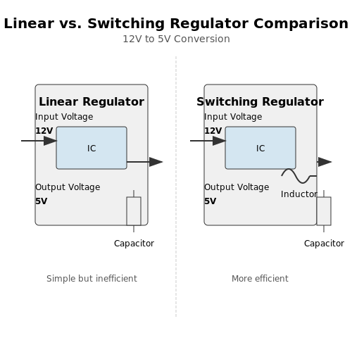
2.2 Capacitors: Types and Their Importance
Capacitors play a crucial role in the functioning of electronic circuits, particularly in power conversion applications such as a 12V to 5V buck converter. Understanding the types of capacitors available and their specific characteristics is vital for selecting the right component for smooth operation and efficiency. Let’s delve into the various types of capacitors and why they are indispensable in this context.
Capacitor Fundamentals
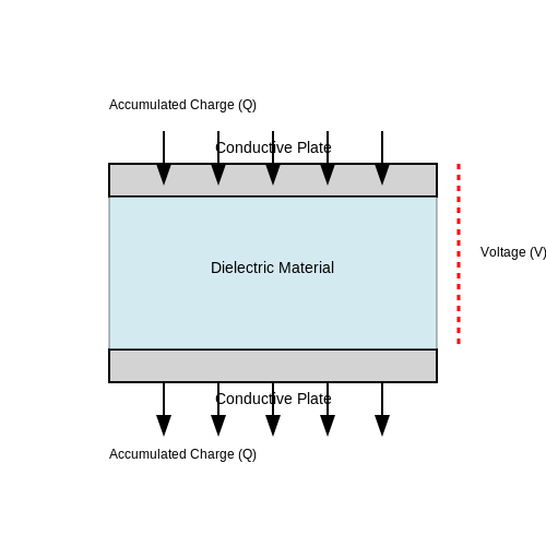
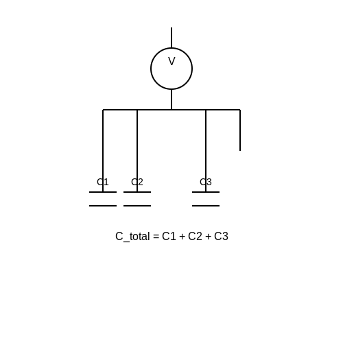
A capacitor is a two-terminal passive component that stores electrical energy in an electric field. The ability of a capacitor to store charge is measured in Farads (F), and it is defined as:
Where C is the capacitance, Q is the charge stored, and V is the voltage across the capacitor. In a buck converter, capacitors are critical for smoothing output voltage and absorbing voltage spikes, hence ensuring stable performance.
Types of Capacitors
Capacitors come in various types, each designed for specific applications and operational conditions. The most relevant types for a buck converter project include:
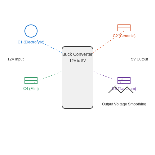
- Electrolytic Capacitors: These are polarized and provide high capacitance values in a relatively small package. They are ideal for bulk energy storage and smoothing in power supply circuits. However, they have limitations in frequency response and are less suitable for high-frequency applications.
- Ceramic Capacitors: Characterized by their low Equivalent Series Resistance (ESR), ceramic capacitors are excellent for high-frequency applications. They are often used in the output stage of buck converters to filter voltage variations. Additionally, they exhibit low leakage, making them reliable for delicate electronics.
- Tantalum Capacitors: With a significantly higher capacitance-to-volume ratio than electrolytics, tantalum capacitors are advantageous for compact designs. They have lower ESR compared to their electrolytic counterparts, ensuring stable performance even under varying loads.
- Film Capacitors: These capacitors provide excellent stability and low losses. While they are typically larger and more expensive than ceramic or tantalum capacitors, their predictable behavior over a wide range of temperatures makes them suitable for certain critical applications in signal processing within converters.
The Importance of Capacitors in Buck Converters
In the context of a 12V to 5V buck converter, capacitors are vital for several reasons:
- Smoothing Output Voltage: Capacitors at the output reduce ripple voltage, ensuring that the voltage supplied to the load is stable. This is particularly important for sensitive electronics that require a steady supply voltage.
- Energy Storage: Capacitors can store energy during periods of low load, ensuring that there is sufficient power available during transient loads.
- Voltage Spikes Protection: Supplying quick bursts of current during load transients prevents damage to both the circuit and the load attached to the buck converter.
Choosing the right combination of capacitors for a buck converter design is an integral part of maximizing efficiency and reliability. Understanding the unique characteristics and limitations of each capacitor type allows engineers to optimize circuit parameters effectively.
2.3 Inductors: Choosing the Right Specifications
In the context of designing a 12V to 5V buck converter, selecting the appropriate inductor is a critical step that significantly influences the efficiency and performance of the converter. Inductors serve as energy storage components during the switching cycle, where they charge when the switch is closed and discharge when it is open. Thus, the configuration has implications not only for the conversion ratio but also for ripple current, efficiency, and thermal management. To begin with, we must understand fundamental parameters associated with inductors that will guide our choice. When selecting an inductor, consider the following specifications:Inductance Value
The inductance value, measured in henries (H), dictates how energy is stored in the magnetic field. The formula to determine the inductance is derived from the basic relationship in inductors:Current Rating
The current rating is just as crucial and is specified as the maximum continuous direct current (DC) that an inductor can handle without saturating. Importantly, saturation can lead to a rapid drop in inductance and overheating. The saturation current \( I_{sat} \) should ideally be greater than the peak current through the inductor, which can be estimated as:DC Resistance (DCR)
The DC resistance of an inductor directly affects the efficiency of a buck converter. Higher resistance leads to increased I²R losses, which generate heat and reduces efficiency. When selecting an inductor, choosing one with minimal DCR while maintaining the required inductance value is essential. It is common practice to select an inductor where the DCR contributes less than a few percent to the total losses.Core Material and Structure
The choice of core material also affects performance, with ferrite cores being popular for higher frequencies due to their low core losses. Conversely, for lower frequency operations, powdered iron cores may be utilized for their high saturation current capabilities. Additionally, the core's shape affects the inductor's saturation characteristics and magnetic field distribution.Inductor Size and Form Factor
Lastly, the physical size and form factor of the inductor can have practical implications in a PCB layout. Larger inductors may handle more current and dissipate heat better but will occupy more board space. Balancing size with electrical performance is crucial in real-world applications. In summary, the selection of inductor specifications in a buck converter circuit revolves around a comprehensive understanding of inductance, current ratings, resistance, core materials, and physical dimensions. When making your choice, consider the specific demands of your application, such as load conditions and efficiency constraints, enabling an optimized design that enhances performance while meeting reliability requirements.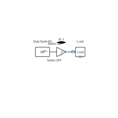
2.4 Diodes and Their Functionality
Diodes are fundamental components in electronic circuits. Their key role is to control the direction of current flow, which is essential in a buck converter circuit, particularly in managing the switching mechanism that converts high voltage to a lower one. Understanding the functionality of diodes in this context is crucial for any engineer or physicist involved in power electronics.
Understanding Diodes
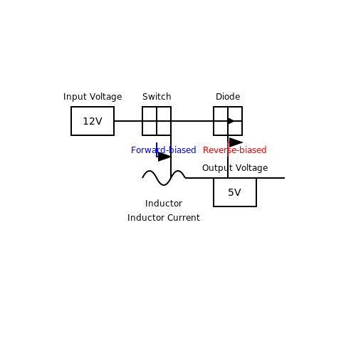
At its core, a diode is a semiconductor device that allows current to flow in one direction while blocking it in the reverse direction. This property arises from its unique construction, typically comprising a P-N junction. When a positive voltage is applied to the anode (the P-type side) relative to the cathode (the N-type side), the diode becomes forward-biased, allowing current to pass through. Conversely, if the cathode is at a higher voltage than the anode, the diode is reverse-biased, and current is blocked.
Key Diode Parameters
Several key parameters define a diode's electrical characteristics:
- Forward Voltage (VF): The minimum voltage required for the diode to conduct current in the forward direction. Typically, this voltage is around 0.7V for silicon diodes.
- Reverse Breakdown Voltage (VBR): The voltage at which the diode will start conducting in the reverse direction. This is a critical parameter, as exceeding this voltage can damage the diode.
- Reverse Recovery Time (trr): The time it takes for the diode to switch from conducting to blocking mode when the current direction is reversed. This is particularly relevant in high-frequency applications.
Diodes in Buck Converters
In the context of a buck converter, diodes play a vital role in managing energy transfer during the switching cycles. When the switch (typically a MOSFET) is closed, energy is stored in the inductor. Once the switch opens, the inductor current must continue to flow. This is where the diode, often referred to as a freewheeling or catch diode, becomes crucial.
As the inductor tries to maintain its current flow, the diode becomes forward-biased, allowing the current to circulate through the inductor and diode instead of being abruptly cut off. This process helps prevent voltage spikes, stabilizing the output voltage (5V in our case) desired in the buck converter.
Selection of Diodes
When selecting diodes for buck converter applications, consider the following:
- Voltage Rating: The diode's breakdown voltage should exceed the maximum voltage in the circuit to avoid failure.
- Current Rating: The diode must handle the maximum current that can flow through it during operation to ensure reliability.
- Forward Recovery Characteristics: Fast-switching diodes such as Schottky diodes are often preferred in buck converters due to their lower forward voltage drop and fast recovery times.
Real-World Applications
Diodes in buck converters are ubiquitous in modern electronic devices, including battery chargers, LED drivers, and power supply units for computers. The efficiency and reliability they provide are essential for the performance of these systems. For instance, in automotive applications, buck converters using diodes help regulate power to various control modules, ensuring stable operation despite varying load conditions.
In summary, understanding the functionality of diodes within a buck converter circuit is vital for engineers and researchers alike. Their ability to manage current flow efficiently is fundamental to achieving the desired electrical characteristics in power supply applications.
3. Schematic Overview
3.1 Schematic Overview
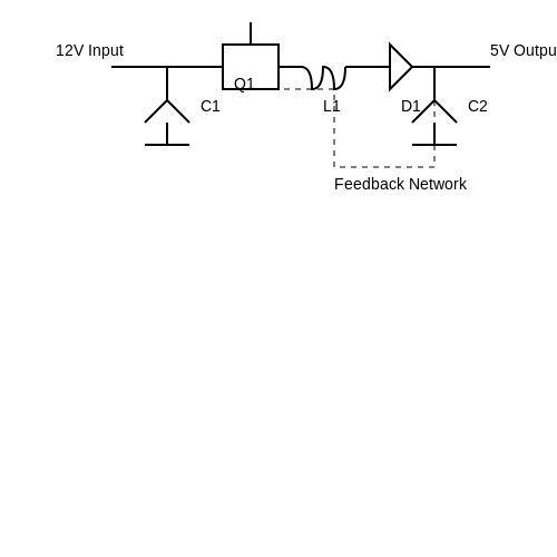
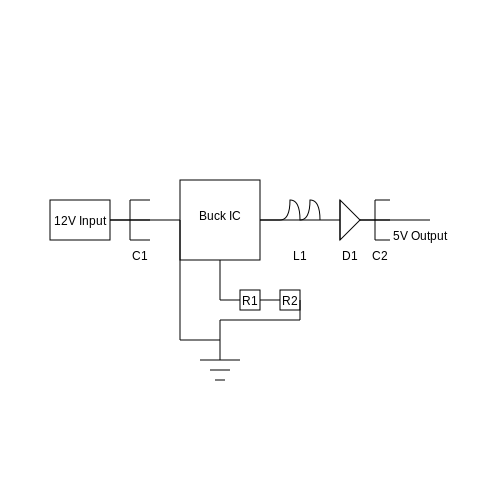
The schematic diagram of a 12V to 5V buck converter offers a visual representation crucial for understanding the fundamental components and their configurations. In a buck converter, the conversion of a higher DC voltage to a lower DC voltage is achieved with notable efficiency, typically reaching up to 95% or more depending on the design. This efficiency makes buck converters highly prized in various applications, from power supplies for consumer electronics to power management systems in renewable energy setups.
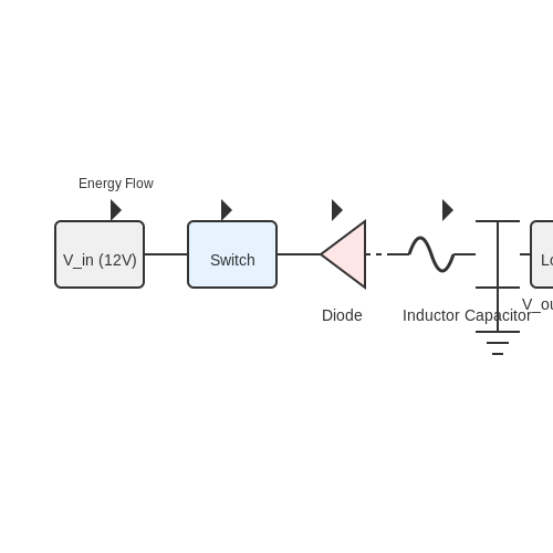
At its core, the buck converter operates using a combination of active and passive components: a switching device (usually a MOSFET), a diode, an inductor, and output filtering capacitors. The switching element intermittently connects the input voltage to the inductor, allowing energy to be stored and released in regulated pulses. During the `on` state, current rises and energy is accumulated in the inductor; during the `off` state, the stored energy is transferred to the load through the diode, ensuring that the output voltage remains stable at the desired level.
Understanding this process requires us to delve into a basic schematic layout:
The schematic features the following components:
- Input Capacitor (C1): This capacitor stabilizes the input voltage by filtering out any high-frequency noise and ripple from the source.
- Switching MOSFET (Q1): The heart of the buck converter, controlling the flow of power at a high frequency, thereby regulating the output voltage through duty cycle manipulation.
- Inductor (L1): Functions as an energy storage component that releases energy to the load during the `off` phase of the switching cycle.
- Diode (D1): Acts as a flyback diode that allows current to flow from the inductor to the load when the switching component is turned off.
- Output Capacitor (C2): Smoothens the output voltage by filtering out any switching noise from the output.
- Feedback Network: Typically composed of resistors, this network senses the output voltage and provides feedback to an integrated circuit that adjusts the MOSFET's duty cycle, ensuring that the output remains at 5V.
The accompanying schematic diagram illustrates these components in their typical arrangement:
This schematic representation effectively summarizes the core components and their interconnections, encapsulating the essential functionalities of the buck converter. The interplay between these components dictates the performance, efficiency, and output stability, which are critical parameters in designing an efficient power supply system.
By leveraging this schematic, engineers and researchers can explore potential modifications to enhance the converter's performance, such as experimenting with different inductor values or implementing advanced feedback control methods to optimize transient response or minimize output ripple.
3.2 Calculating Component Values
In designing a buck converter that steps down 12V to 5V, accurate calculation of component values is crucial for optimizing efficiency, stability, and performance. The primary components involved in a buck converter include the inductor, capacitor, diode, and the switching element, which typically uses a duty cycle for modulation. This section will guide you through the systematic approach to calculating these values, ensuring your design functions effectively under expected load conditions. To start, let’s revisit the basic operation of a buck converter. The converter operates by switching on and off, effectively modulating the input voltage. When the switch is closed, the inductor stores energy, and when it opens, this stored energy is transferred to the load through a diode. The switching frequency and duty cycle significantly influence the performance and output voltage. Inductor Selection The inductor is fundamental in determining the output current ripple and voltage regulation performance. The value of the inductor \(L\) can be estimated using the formula: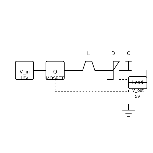
3.3 PCB Design Considerations
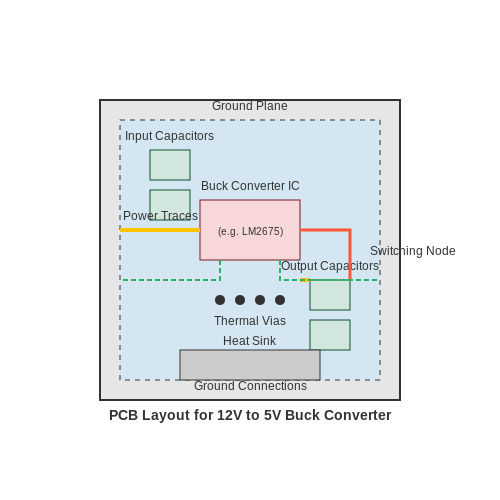
Designing a printed circuit board (PCB) for a 12V to 5V buck converter involves several critical aspects that not only influence the operational efficiency of the converter but also affect its overall reliability and usability. Given the intricate nature of switching regulators, a keen focus on layout, component selection, and thermal management is essential. This subsection delves into these PCB design considerations, offering insights geared towards advanced readers and professionals in the field.
Component Placement
The arrangement of components on the PCB is foundational to the performance of the buck converter. While designing the board layout, the following guidelines should be observed:
- Input and Output Filtering: Position input capacitors as close as possible to the input pin of the buck converter IC. Similarly, place output capacitors near the output pin to minimize the parasitic inductance, which affects the transient response.
- Ground Plane: Employ a solid ground plane to minimize ground impedance. This approach helps to reduce noise and ensures stable operation.
- Switching Node Layout: The switch node (usually the connection point for the inductor and the switching transistor) should be short and direct to prevent inductive losses and voltage spikes that could affect performance.
Trace Width and Current Capacity
Electrical traces on the PCB must be sized correctly to handle the load current without excessive heating. The trace width can be calculated through appropriate formulas or online calculators, factoring in the desired temperature rise and the ambient environment. As a reference, the IPC-2221 standard provides guidelines for determining safe trace widths based on current capacity.
Example Calculation of Trace Width
Assuming a maximum current of 3A and a maximum temperature rise of 10°C, you can estimate the required trace width using the formula:
Where:
- I: Current in Amperes
- Tmax: Maximum allowable temperature
- Tambient: Ambient temperature
- k: Constant based on the desired trace capabilities
- n: A material property constant
This calculation ensures trace integrity under load conditions and prevents potential overheating issues.
Thermal Management
Power converters generate heat, and proper thermal management is vital to prevent overheating, which can lead to component failure. Employing the following techniques will enhance thermal performance:
- Thermal Vias: Utilize thermal vias connected to the ground plane to dissipate heat from power components. This method increases the heat transfer area.
- Heat Sinks: If necessary, incorporate heat sinks on critical components with significant thermal dissipation, such as the MOSFETs used in the buck converter.
- Component Selection: Opt for components rated for high temperatures. Consider MOSFETs with low on-resistances (RDS(on)) to minimize heat generation during operation.
Simulation and Testing
It is prudent to simulate the PCB design using software tools such as SPICE or PCB design software that includes simulation capabilities. Evaluate aspects such as thermal performance, transient response, and noise behavior. After the initial prototype, thorough testing and analysis can identify potential issues in real-world applications.
The integration of these considerations offers a holistic approach to the PCB design process for a 12V to 5V buck converter. By meticulously planning the layout, selecting appropriate components, and addressing thermal issues, engineers can significantly enhance the performance and reliability of their power conversion designs.
4. Required Tools and Equipment
4.1 Required Tools and Equipment
Creating a 12V to 5V buck converter is not only an essential skill for electronics enthusiasts, but also an opportunity to engage with core concepts in circuitry and energy conversion. To embark on this DIY project, you'll need to gather an array of tools and equipment that are pivotal for ensuring precision and safety during assembly. Below, we outline a comprehensive list tailored for advanced-level readers, emphasizing the importance of each item.
Essential Electronic Components
At the heart of any buck converter are key components that dictate its performance. The following is a rundown of essential electronic parts you will require:
- Inductor: Typically in the range of 10 µH to 100 µH, the inductor stores energy during the switching cycle and releases it when the switch is off.
- Capacitors: Both input and output capacitors stabilize voltage and reduce ripple. Look for ceramic or electrolytic capacitors with suitable voltage ratings.
- Diode: A Schottky diode is recommended due to its low forward voltage and fast recovery time, minimizing conduction losses.
- Switching Device: An efficient power MOSFET rated for high current levels is crucial; its on-resistance influences the overall efficiency of the converter.
- Controller IC: A dedicated buck converter controller (e.g., LM2596) simplifies the process significantly, enabling regulated output voltage control.
Tools for Assembly
Proper assembly requires precision; thus, having the right tools is essential. Here’s what you’ll need:
- Soldering Iron: A quality soldering iron with a fine tip is indispensable for soldering components onto the PCB reliably.
- Solder: Use high-quality solder with a rosin core, ideally 0.6-0.8 mm diameter, which ensures good electrical connections.
- Wire Cutters and Strippers: For trimming leads post-soldering and preparing wires for connections.
- Multimeter: Essential for measuring voltage, current, and resistance, allowing you to troubleshoot and validate the circuit.
- Oscilloscope: For visualizing the output voltage waveform, enabling you to assess ripple and transient responses critically.
Workspace Considerations
A clean, organized workspace enhances productivity and safety. Ensure that your working area has:
- Anti-static Mat: Protects sensitive components from electrostatic discharge (ESD).
- Good Lighting: Facilitates detailed work, especially during soldering and assembly stages.
- Storage Containers: Helps keep components organized and easily accessible, reducing the risk of losing small parts.
Safety Equipment
Safety should never be overlooked, especially in projects involving electrical components:
- Safety Goggles: Protects your eyes from solder splatters and dust.
- Heat-resistant Gloves: Useful when handling hot components or solder.
Equipped with the right tools and components, you're now ready to dive deeper into understanding the design and functionality of a 12V to 5V buck converter. This groundwork will ultimately enhance your ability to create efficient energy conversion systems pertinent in various electronic applications, from consumer electronics to advanced automotive systems.
4.2 Step-by-Step Assembly Instructions
The process of assembling a 12V to 5V buck converter involves a series of precise and methodical steps that ensure a functional and efficient power supply. This tutorial presumes familiarity with basic electronic components and circuit assembly techniques, as it caters to an advanced audience.
Materials Required
Before starting the assembly, ensure you have the following components at hand:
- Buck Converter IC: An efficient switching regulator IC such as LM2596 is preferable.
- Inductor: A suitable inductor (e.g., 33μH) rated for at least 3A current.
- Capacitors: Input capacitor (10μF), output capacitor (100μF), and a small ceramic capacitor (10nF) for noise filtering.
- Diode: A Schottky diode (e.g., 1N5819) to prevent reverse current.
- Resistors: Two resistors to set the output voltage.
- PCB or Breadboard: For assembling the circuit.
- Connecting Wires: For making connections between components.
- Multimeter: For measuring voltage and current during testing.
Step 1: Understanding the Circuit Diagram
Before beginning assembly, it's essential to familiarize yourself with the circuit diagram of the buck converter. The circuit generally consists of an input voltage source connected to the buck converter IC, which regulates the output voltage through the inductor and capacitors.
The configuration essentially works as follows:
- The input voltage (12V) is connected to the input of the buck converter IC.
- The IC switches on and off rapidly, storing energy in the inductor.
- When the switch is off, the inductor discharges its stored energy through the output capacitor, providing a regulated 5V output.
Step 2: Assembling the Components
Begin by positioning the components on the PCB or breadboard according to the circuit diagram. Pay special attention to:
- Correctly orienting polarized components such as capacitors and diodes.
- Securing the buck converter IC onto the PCB, ensuring it is soldered properly to avoid cold joints.
Step 3: Making Connections
Using the connecting wires, adhere to the wiring schematic carefully. Ensure the following:
- All connections are tight and free from short circuits.
- Follow the recommended trace width on the PCB for high current paths to prevent overheating.
Step 4: Testing the Circuit
Before powering the circuit, perform a visual inspection to confirm that all components are placed correctly and no shorts exist. Then proceed with the following testing method:
- Set the multimeter to DC voltage mode.
- Power the circuit and measure the output voltage across the output capacitor terminals.
- If the voltage is not close to 5V, check the connections, especially around the feedback resistors which set the output voltage of the buck converter.
Step 5: Troubleshooting Common Issues
If issues arise during testing, consider the following:
- Incorrect output voltage due to an error in resistor values.
- Heating of components indicating overcurrent conditions; check load specifications.
- No output voltage caused by improper IC orientation or failed components.
Once you've verified the functionality of your buck converter with stable output, encapsulating the circuit in an enclosure can protect it from environmental factors, ensuring reliable long-term operation.
With your 12V to 5V buck converter successfully assembled, you can now leverage its functionality for various applications, such as powering microcontrollers or charging small batteries, all while benefitting from increased efficiency and reduced heat output compared to linear regulators.
4.3 Testing the Assembled Circuit
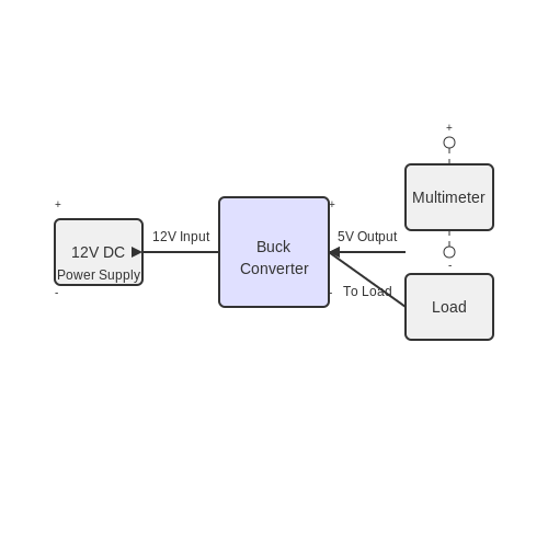
Once the 12V to 5V buck converter has been carefully assembled on the PCB and all connections verified, the next critical step involves testing the circuit to ensure it operates as expected. Testing not only verifies functionality but also checks for stability under various load conditions. Here are the systematic steps you should follow for effective testing.
Initial Power-Up Test
The first step is to connect your buck converter to a stable 12V DC power supply while ensuring that there are no loads attached to the output. This initial test aims to confirm that the circuit powers on without any issues.
- Connect the power supply: Verify that the positive terminal of the 12V supply goes to the input '+' of the buck converter, and the negative terminal to the input '−'.
- Power on: Switch on the power supply while monitoring the circuit for any excessive heat or smoke.
If the circuit powers up without any anomalies, you can proceed to measure the output voltage.
Measuring Output Voltage
With the circuit powered, utilize a multimeter to measure the output voltage across the output terminals.
- Set the multimeter: Ensure the multimeter is set to the DC voltage range appropriate for 5V.
- Probe the output: Connect the multimeter probes to the output terminals of the buck converter.
The measured voltage should ideally be around 5V. If the voltage is significantly lower or higher than expected, inspect the circuit for issues such as incorrect component values, faulty components, or wiring errors.
Load Testing
Next, it's essential to test the converter under actual operational conditions by applying a load to the output. This step ensures that the converter can handle real-world applications and maintains stable output voltage.
- Select a load: Choose a resistive load that draws current not exceeding the rated output current of your buck converter.
- Connect the load: Attach the load across the output terminals of the buck converter.
Observe the output voltage once the load is applied. Ideally, the voltage should remain around 5V despite load changes. Monitor the circuit's temperature as well; excessive heat may signal inefficiencies or overload conditions.
Efficiency Testing
Efficiency is a crucial parameter in power conversion circuits. To calculate the efficiency of your buck converter, you will need to measure both the input and output voltage and current.
Where:
- Pout: The output power, calculated as Vout × Iout.
- Pin: The input power, calculated as Vin × Iin.
For accurate results, ensure that you are measuring under steady-state conditions and consider taking multiple readings to average out any fluctuations. In practical applications, efficiencies above 85% are typically expected for well-designed buck converters.
Final Considerations
After completing all tests, review your results. If the circuit performs well under all conditions, you can proceed to utilize the buck converter in your electronic projects. Document any observations and measurements for future reference and potential troubleshooting.
This testing phase is essential for ensuring that the DIY buck converter is reliable, efficient, and suitable for your intended application.
5. Identifying Power Loss
5.1 Identifying Power Loss
In the design of a 12V to 5V buck converter, power loss is a critical aspect that can significantly affect overall efficiency. Understanding the sources of power loss not only allows for the design of more efficient converters but also contributes to the longevity and reliability of the system. Power loss in a buck converter can primarily be categorized into three types: conduction losses, switching losses, and gate drive losses. Each type of loss is influenced by various parameters, including the characteristics of the components used in the circuit, operating conditions, and the overall design of the converter.Conduction Losses
Conduction losses occur due to the resistance of the components when current flows through them. The most significant contributors to conduction losses in a buck converter are the MOSFETs, inductor, and output capacitor. The power loss associated with the MOSFET can be quantified using the formula:Switching Losses
Switching losses arise during the transitions of the MOSFETs between their on and off states. These losses depend on the switching frequency and the voltage across the device during the switching event. The power loss due to switching can be represented as:Gate Drive Losses
Gate drive losses occur primarily due to the energy required to charge and discharge the gate capacitance of MOSFETs. These losses become particularly significant at high switching frequencies. This contribution to power loss is often calculated using the equation:Practical Implications
The power loss in a buck converter is a multi-faceted issue requiring careful design considerations. Engineers should assess the thermodynamic effects of power losses since elevated temperatures can lead to component degradation and reduced reliability over time. Moreover, understanding these losses allows for optimization strategies, such as choosing advanced materials, implementing synchronous rectification, or using low-resistance inductors, to enhance the converter's efficiency. In applications where power efficiency is paramount, such as in portable electronics and renewable energy systems, minimizing these losses translates directly into better performance and prolonged operational lifespan. By systematically identifying the sources of power loss, engineers can create improved design iterations of buck converters, thereby enhancing efficacy while keeping thermal and cost constraints in check.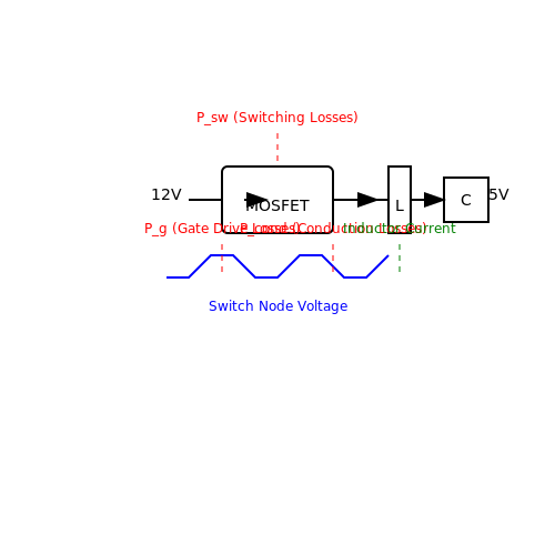
5.2 Diagnosing Output Voltage Issues
In the design and application of a 12V to 5V buck converter, output voltage issues can significantly impact efficiency and circuit performance. Likewise, understanding the root causes of these issues is vital for a successful troubleshooting approach. High-frequency switching converters, such as buck converters, are susceptible to various sources of errors and anomalies that require careful investigation. To begin, let’s consider the common symptoms associated with output voltage discrepancies. A buck converter might produce a voltage that deviates from the expected 5V, exhibiting either a surplus (overvoltage) or a deficit (undervoltage). Understanding these conditions necessitates a look at the fundamental principles governing the device's operation. One common cause of output voltage issues is inadequate load regulation. This means that fluctuations in the load can lead to variations in output voltage. Implementing proper feedback control is critical for stabilizing output against load changes. An error amplifier can be utilized to compare the output voltage with a reference voltage, allowing for necessary adjustments to ensure regulation. Moreover, examining the switching frequency and the component selection is paramount. The switching frequency affects both output ripple and transient response. If the frequency is too low, the converter may not maintain the desired voltage under variable loads. Conversely, too high a frequency can lead to increased switching losses. The relationships between these variables can be articulated through the equations governing the converter's operational states. Whenever we deal with output discrepancies, ripple voltage should also be analyzed. Ripple arises from the charging and discharging of the output capacitor during the on-off cycles of the switching element. A higher output ripple could indicate insufficient capacitance or poor PCB layout that leads to increased inductance. To accurately evaluate this, one can mathematically derive the ripple voltage equation based on capacitor charge cycles and current loads: The equation governing output ripple, \( V_{\text{ripple}} \), can be formulated from: $$ V_{\text{ripple}} = \frac{I_L}{f_S \times C} $$ where \( I_L \) is the load current, \( f_S \) is the switching frequency, and \( C \) is the capacitance. This relationship highlights how higher frequencies or larger capacitance can mitigate ripple voltage. In addition to load regulation and ripple voltage, other potential culprits could include improper component tolerances, especially in critical components like MOSFETs and diodes, or layout issues that introduce parasitic inductance and resistance. Utilizing an oscilloscope can provide real-time feedback of output voltages, allowing engineers to visualize discrepancies under various load conditions. In the field, real-world application requires a robust approach to mitigate these issues. For instance, implementing temperature compensation within feedback circuits and using high-quality components designed for level-shifting power applications is essential for maintaining stable output voltages across various environmental conditions. In conclusion, diagnosing output voltage issues in a 12V to 5V buck converter involves a comprehensive assessment of dynamic load conditions, switching frequency, output ripple, and component specifications. A meticulous approach to both theoretical calculations and practical measurements is indispensable for enhancing converter performance and reliability.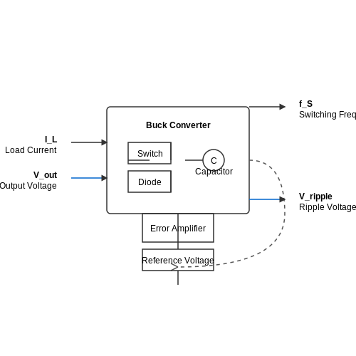
5.3 Resolving Noise and Ripple Problems
The principles of power conversion, particularly when stepping down voltages in applications like a 12V to 5V buck converter, invariably introduce challenges such as unwanted noise and voltage ripple. These challenges can significantly affect the performance of sensitive electronic devices. Therefore, understanding how to effectively mitigate these issues is central to improving the reliability and efficacy of buck converter circuits.
Understanding Noise and Ripple
To establish a firm foundation, it's essential to differentiate between noise and ripple. Noise typically refers to high-frequency voltage fluctuations that can interfere with signal integrity, while ripple refers to the residual periodic variation in the output voltage that occurs after rectification and smoothing. Both phenomena can stem from various factors, including switching frequency, load variations, and electromagnetic interference (EMI).
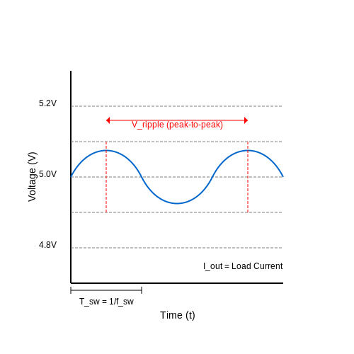
Ripple Analysis
The ripple voltage in a buck converter is primarily influenced by the output capacitor's characteristics and the inductor's current ripple. The ripple can be modeled mathematically using the following relations, which are foundational for designing appropriate filtering solutions.
Where:
- Vripple is the peak-to-peak ripple voltage.
- Iout is the output load current.
- fsw is the switching frequency of the converter.
- Cout is the output capacitance.
This equation illustrates that increasing the capacitance or the switching frequency can help reduce ripple. However, electrical engineers must balance these factors with component size and cost considerations, leading to trade-offs in design.
Noise Mitigation Techniques
To effectively combat noise in buck converters, several techniques can be employed:
- Proper PCB Layout: Ensuring short, low-inductance paths for high-frequency switching currents is crucial. Ground planes and proper placement of components can minimize loop areas, reducing radiated noise.
- Decoupling Capacitors: Place ceramic capacitors close to the load to act as high-frequency filters. Their low equivalent series resistance (ESR) and equivalent series inductance (ESI) allow them to respond quickly to voltage transients.
- Ferrite Beads: Inserting ferrite beads in series with power lines can impede high-frequency noise without significantly affecting the desired DC voltage.
- RC Filtering: An additional low-pass filter consisting of a resistor and capacitor can further smooth out voltage outputs and reduce ripple. The cutoff frequency (\(f_c\)) can be determined as follows:
Where \(R\) is the resistance and \(C\) is the capacitance. Proper selection of these components allows engineers to customize the filtering characteristics to suit specific applications.
Practical Considerations and Testing
When implementing these techniques, testing and measurement play an indispensable role. Engineers should utilize oscilloscopes with appropriate bandwidth and capture the output both at varying load conditions and across different instances. This ensures that the designed solution effectively meets the intended specifications under real-world operating conditions.
In conclusion, designing a buck converter that efficiently minimizes both noise and ripple involves a multifaceted approach that combines theoretical principles with practical implementation strategies. As advancements in electronics continue, ongoing improvements in materials and design practices will provide even greater performance in power conversion applications.
6. Working with Low Voltage
6.1 Working with Low Voltage
In the realm of power electronics, working with low voltage applications requires a firm grasp of both circuit behaviors and component limitations. As we delve into the intricacies of the 12V to 5V buck converter, understanding the principles behind low voltage operations is crucial for efficiency, reliability, and performance.
Low voltage applications typically involve voltages less than 50V, which, while safer in certain contexts, present unique challenges such as increased susceptibility to noise, r ripple management, and thermal considerations. These factors significantly affect the overall system design and the selection of circuit components.
Principles of Low Voltage Operation
When designing circuits intended to operate at lower voltage levels, you will face several considerations:
- Efficiency: Power loss in the form of heat is a principal concern. At low voltages, even small losses can have significant impacts on overall efficiency.
- Ripple Control: The output voltage ripple becomes a critical parameter, particularly in applications like microcontrollers that require stable power supplies.
- Drive Capability: Many power components, such as MOSFETs and BJTs, have specific minimum gate-source voltages and other parameters that must be carefully selected to ensure they function as intended.
Voltage Regulation Techniques
Maintaining a stable output voltage in low voltage applications often necessitates the implementation of effective voltage regulation techniques. Among these, feedback mechanisms are commonly used. These can range from basic linear voltage regulators to sophisticated switch-mode power supplies (SMPS).
For a buck converter, it is essential to utilize appropriate feedback loops that monitor and adjust the output voltage based on load variations. The feedback can be analyzed mathematically, incorporating the expected load and component specifications to derive essential operational characteristics.
Mathematical Modeling of the Buck Converter
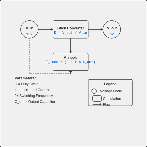
To understand the behavior of a buck converter at low voltages, we derive the relationship between input and output voltages through simple circuit equations. The average output voltage \( V_{out} \) of a buck converter is related to the input voltage \( V_{in} \) and the duty cycle \( D \) as follows:
Where the duty cycle \( D \) represents the fraction of the switching period during which the switch is in the 'on' state. By analyzing the system under varying loads, we can further determine the ripple voltage \( V_{ripple} \) at the output:
This equation showcases the fundamental relationship between load current, switching frequency, and output capacitor value for maintaining desired ripple specifications.
Real-world Applications
In practice, low voltage operations are vital in numerous applications including:
- Consumer Electronics: Devices like smartphones and tablets rely heavily on efficient, compact buck converters for battery management.
- Automotive Systems: Modern vehicles utilize low voltage power supplies to minimize weight and improve energy efficiency.
- Embedded Systems: Microcontrollers and processors often require stable low voltage supply rails to function optimally.
Engaging with low voltage challenges not only improves one’s design acumen but also enhances the performance and longevity of electronic systems. By understanding the intersection between theory and practical implications in low voltage applications, engineers and researchers can develop innovative solutions to meet current and future demands.
6.2 Preventing Component Damage
The successful implementation of a 12V to 5V buck converter requires not only a deep understanding of circuit functionality but also a keen awareness of potential damage to components. As we shift our focus to safeguarding the health of these intricate circuits, we unravel the importance of meticulous design, optimal component selection, and protective mechanisms.
Components within our buck converter, such as inductors, capacitors, diodes, and MOSFETs, are highly sensitive to electrical stresses. Exceeding their rated voltages or currents can lead to catastrophic failures. Thus, understanding the operational limits and protective methodologies is crucial to maintain circuit integrity.
Understanding Component Ratings
Every electronic component comes with defined maximum ratings for voltage and current, typically detailed in their datasheets. For instance, a MOSFET specified for a maximum drain-source voltage (VDS) of 30V should never encounter voltages exceeding this limit to avoid breakdown. Similarly, for inductors and capacitors, applying voltages beyond their ratings can result in overheating and eventual failure.
Derivation of Safety Margins
When designing circuits, it is prudent to apply a safety factor to these ratings. A common practice is selecting components that can handle at least 20% to 30% greater than expected operating conditions. Let's consider a practical calculation; if a MOSFET operates at a maximum current of 10A under normal conditions, a desired rating for safety might be:
This practice not only increases reliability but also comfortably accommodates transient conditions, such as load surges or unexpected voltage spikes.
Implementing Protection Circuits
A well-designed buck converter should incorporate protection mechanisms such as fuses, diodes, and _voltage clamping_ devices:
- Fuses can limit the current and prevent excessive heating or component damage.
- Schottky diodes can be used for flyback protection, effectively managing the reverse polarity of inductive loads.
- Transient Voltage Suppressors (TVS) can absorb voltage spikes, protecting sensitive elements within the circuit.
Practical Example: Overcurrent Protection
To implement a basic overcurrent protection mechanism, integrating a fuse rated slightly above the expected load current into the circuit is essential. For instance, if your circuit consistently draws 3A, a fuse rated at 4A would provide adequate protection.
Thermal Management Strategies
Heat generation is an inevitable aspect of power conversion, primarily due to resistive losses in components. Understanding thermal resistance is key to developing an efficient cooling strategy. The thermal resistance, θJA, can be calculated from the datasheet for components like transistors and is typically defined as:
Here, \(T_{j}\) is the junction temperature, \(T_{a}\) is the ambient temperature, and \(P_{D}\) is the power dissipation.
To manage thermal energy, options include:
- Using heat sinks or thermal pads to dissipate heat.
- Employing active cooling methods like fans for high-power applications.
Each strategy enhances performance and extends the lifespan of your buck converter circuit by ensuring components operate within recommended temperature limits.
Final Thoughts
In conclusion, adopting a well-rounded approach to prevention is essential for prolonging component lifespan in a DIY 12V to 5V buck converter. Understanding component ratings, implementing protective measures, and managing thermal issues effectively contribute to a reliable power conversion system. As you further develop your buck converter, incorporating these strategies will lead to improved performance and durability.
6.3 Ensuring Personal Safety
In the context of building a 12V to 5V buck converter, personal safety becomes paramount. Working with electronics frequently involves handling voltages that can be hazardous, especially in DIY projects. While the operational voltages in a buck converter may be relatively modest, it is crucial to approach construction and experimentation with a mindful perspective on safety protocols. To understand how to ensure personal safety, we must first recognize potential hazards associated with electronic components, particularly regarding high voltage, capacitors, and thermal management. High voltage can lead to severe electrical shocks, while improperly handled capacitors may still retain charge long after power is disconnected, leading to a risk of injury.Electric Shock and Circuit Integrity
When working on a buck converter, any unintended short circuits or component failures can expose you to electric shock. The primary sources of these shocks are often the input voltage terminals. Using insulated tools and wearing rubber-soled shoes while working on the project can mitigate risks. Additionally, ensuring that your workspace is dry and free from conductive materials is essential. You should also use a multimeter to verify circuit integrity before powering up your device. This step is vital to detect any faults, which, if left unchecked, could lead to catastrophic failures. For practical implementation:- Always power down and disconnect your circuit before making any adjustments.
- Use insulated connectors to reduce the risk of accidental short-circuits and ensure stable connections.
- Employ a programmable power supply with current limiting features, as this can help prevent damage during initial testing.
Capacitor Discharge Procedures
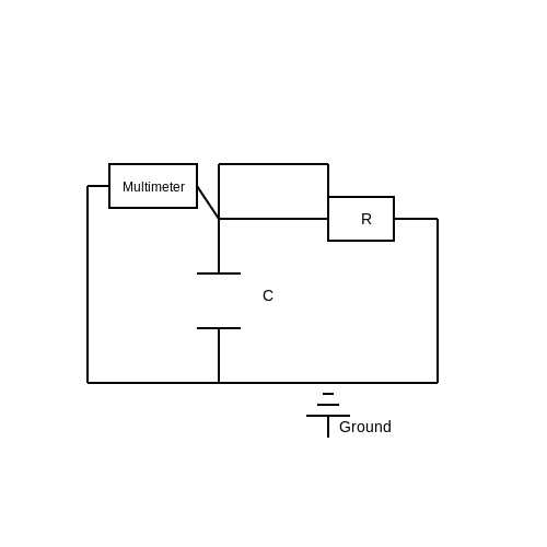
One of the primary components in a buck converter circuit is the capacitor. Capacitors can store charge well beyond the operational state of the circuit, posing a risk of electric shock. It is imperative to develop a proper capacitor discharge protocol. Before working on the circuit:- Use a resistive discharge method to safely deplete capacitor charge. This involves connecting a resistor across the capacitor's terminals to dissipate stored energy gradually.
- Always test the capacitor with a multimeter after discharge procedures to ensure that no residual voltage remains.
Thermal Management and Fire Safety
Another critical aspect of safety involves thermal management. Power conversion can result in substantial heat generation in buck converters, especially under high-load conditions. This heat can potentially lead to component failure or even fires if not effectively managed. To mitigate these risks:- Utilize appropriate heatsinks or active cooling systems for high-power applications.
- Monitor the temperature of the circuit during operation to ensure it remains within defined limits. Temperature sensors may be integrated for automated safety shut-offs.
7. Recommended Books
7.1 Recommended Books
- Switching Power Supply Design & Optimization — This book offers an in-depth guide to the design principles of switching power supplies, which are essential for creating efficient buck converters. It includes practical design examples and optimization techniques.
- Power Electronics: Principles and Applications — A comprehensive text covering the principles of power electronics including design and analysis of converters like buck converters, with applications oriented toward real-world scenarios.
- Handbook of Power Management Circuits — This resource delves into advanced power management circuits with a focus on efficiency, covering buck converters in depth to address 12V to 5V conversion challenges and solutions.
- Design of Analog Filters — While focused primarily on filters, this book provides fundamental insights into the circuit elements used in power converters, including those used in buck converters.
- Power Electronics: Converters, Applications, and Design — This comprehensive guide offers detailed coverage of buck converters, including mathematical models and design procedures, supported by real-world examples.
- Modern Power Electronics — An insightful look into modern power electronics components and systems with substantial focus on DC-DC converters, including the theory and design of buck converters.
- Power Supply Cookbook — A practical book providing easy-to-follow steps for designing power supplies, including buck converters, making complex concepts accessible and applicable.
7.2 Online Resources and Tutorials
- Understanding Buck-Boost Power Stages in Switch Mode Power Supplies — A comprehensive document from Texas Instruments that delves into the operational principles and design techniques for buck and boost converters, including theoretical insights and practical applications.
- DC to DC Converter Tutorial — This site offers detailed explanations of DC-DC converters, with a specific section dedicated to buck converters. It covers key concepts such as voltage regulation, switching, and energy efficiency.
- All About Circuits: Switched-Mode Power Supplies — Explore an in-depth tutorial on switched-mode power supplies, focusing on buck converters. This resource includes circuit diagrams, equations, and practical design tips.
- Designing DC-DC Converters — A technical article that addresses the design considerations for creating efficient DC-DC converters, including buck converters. Key topics include component selection and thermal management.
- Intro to Buck Converters — This application note by Maxim Integrated introduces buck converter technology with practical insights, tips for improving efficiency, and detailed schematics.
- YouTube: Buck Converter Tutorial — A visual guide demonstrating the construction and testing of a buck converter. This video tutorial effectively bridges theory and practice by showing real-world application.
- Build Your Own Buck Converter — EDN provides a DIY guide for constructing a buck converter from scratch, complete with a parts list, schematic, and step-by-step instructions.
- DIY Hacking: What Are Buck & Boost Converters? — This article introduces buck and boost converters with a focus on hobbyist projects. It provides foundational knowledge alongside practical examples.
- Circuit Digest: The Basics of Buck Converters — A beginner-to-advanced guide on buck converters, covering theoretical concepts and practical design strategies. It includes schematics and component analysis.
7.3 Relevant Academic Papers
- A 12 V-to-5 V Buck Converter Design — This paper presents a theoretical model and practical design considerations for constructing a 12V to 5V buck converter, focusing on efficiency and output stability.
- High-Efficiency Buck Converter Design — Focuses on enhancing the efficiency of buck converters through innovative topologies. Suitable for researchers looking to minimize power loss in buck converter circuits.
- Optimization Techniques for Buck Converter Circuits — Explains various optimization techniques applicable to buck converter design, including selection of components for optimal performance.
- PWM Control in Buck Converters — Discusses advanced Pulse Width Modulation (PWM) techniques in the context of buck converters, emphasizing the importance of control strategies for voltage regulation.
- Analysis of Losses in Buck Converter Designs — Provides insights into different types of losses encountered in buck converters and suggests methods to minimize these losses to enhance efficiency.
- Thermal Management in Buck Converters — Addresses the challenges of thermal management in buck converters and investigates cooling techniques to prevent overheating.
- Dynamic Modeling of Buck Converters — Focuses on the dynamic behavior of buck converters, exploring the impact of load variations and component non-idealities on performance.
- Switching Frequency Analysis in Buck Converters — Analyzes the effect of switching frequency on the efficiency and size of buck converters, providing practical guidelines for selecting appropriate frequencies.