Buck Converter
1. Definition and Purpose
1.1 Definition and Purpose
In the realm of power electronics, the buck converter stands as a pivotal component for efficient voltage regulation. It serves the primary purpose of stepping down voltage from a higher level to a lower one while maintaining energy conservation principles—a crucial requirement in modern electronic devices.
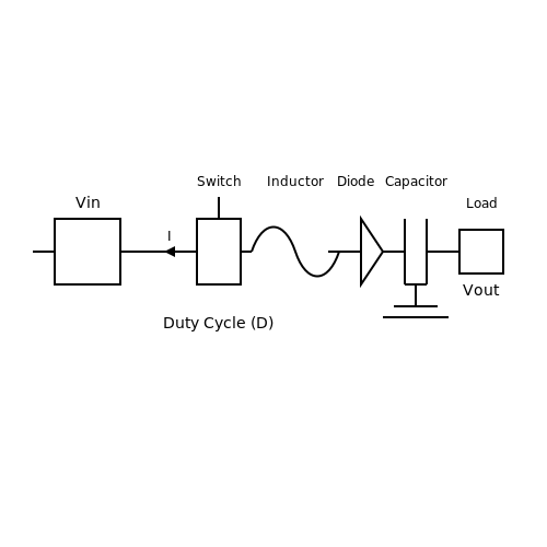
The buck converter, often classified as a DC-DC converter, employs a straightforward yet ingenious mechanism involving an inductor, switch (transistor), diode, and output capacitor. When the switch is closed, current flows through the inductor, which stores energy temporarily. As the switch opens, this stored energy is released to the output through the diode, thus decreasing the voltage and ensuring that the load receives a stable and regulated output voltage.
Operational Principle
The operational principle of the buck converter is based on the concept of duty cycle, defined as the ratio of the on-time of the switch to the total cycle time. This relationship determines the average output voltage. Mathematically, we can express the output voltage (\( V_{out} \)) of a buck converter relative to the input voltage (\( V_{in} \)) as:
Here, \( D \) is the duty cycle, ranging from 0 to 1. For instance, if \( D = 0.5 \) and \( V_{in} = 12V \), the output voltage will be \( V_{out} = 0.5 \cdot 12 = 6V \).
Applications and Relevance
As a result of its efficiency and compact design, the buck converter is widely utilized in various applications, including:
- Renewable Energy Systems: Integration in solar inverters to convert the variable DC output of solar panels into stable, usable power.
- Battery-Powered Devices: Essential for devices requiring efficient energy conversion to extend battery life.
- Telecommunications: Used in powering RF circuits and other sensitive components needing a stable supply voltage.
- Consumer Electronics: Found in mobile phones, laptops, and other personal devices to manage power efficiently.
Moreover, the buck converter is pivotal in applications where weight and space are critical factors, such as in aerospace and automotive sectors. Its ability to operate with minimal heat generation additionally aids in thermal management, which is crucial for reliability in various environments.
In summary, the buck converter exemplifies an essential technology in modern electronics, allowing engineers to create products that are both energy-efficient and performance-oriented. As technology advances, the role of buck converters is likely to expand, influencing new designs and innovations.
1.2 Operating Principle
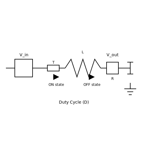
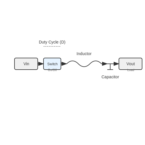
In order to comprehend the operating principle of a buck converter, it is essential to grasp the fundamental concepts of voltage regulation, switching power supplies, and energy transfer. The buck converter, a type of DC-DC converter, is designed specifically to efficiently reduce a higher input voltage to a lower output voltage, thus supporting a variety of applications ranging from power supply for electronic devices to renewable energy systems. At its core, the buck converter operates on the principle of energy storage and release through an inductor and a switching device — usually a transistor. The process begins with the transistor acting as a controlled switch. When the switch is closed (ON state), current flows through the inductor, causing the inductor to store energy in the form of magnetic field. This phase is characterized by a linear increase in current through the inductor, and the voltage across it can be described by the equation:The operational principle of a buck converter, illustrating the switch, inductor, and output load configuration.
1.3 Components of a Buck Converter
The design and operation of a Buck Converter hinge on a few fundamental components, each playing a distinct role in facilitating efficient voltage regulation. Understanding these components is crucial for optimizing the converter's performance in both theoretical and practical applications, ranging from power supplies in electronics to renewable energy systems.Switching Device
At the heart of every Buck Converter is the switching device, typically a *MOSFET* (Metal-Oxide-Semiconductor Field-Effect Transistor) or an IGBT (Insulated Gate Bipolar Transistor). This component acts as a gatekeeper, rapidly opening and closing to control the flow of electrical energy from the input to the output. The switching frequency is a critical parameter, affecting the efficiency and size of the converter. The MOSFET is often preferred due to its high efficiency and fast switching capabilities. The choice of switching device directly impacts the thermal management of the converter, as higher switching losses result in more heat generation. Therefore, selecting a device with a low on-resistance and fast switching speed is essential for minimizing losses.Diode
Complementing the switching device, the diode (often a Schottky diode for its low forward voltage drop and fast recovery time) is employed in the Buck Converter to provide a path for the inductor current when the switch is off. This is known as the *freewheeling* or *catch* diode function. Its rapid switching ability ensures continuous current flow, preventing voltage spikes that could damage the converter. In applications where efficiency is paramount, synchronous rectification may be implemented, replacing the diode with a secondary switching device (often a MOSFET). This method further reduces losses associated with the diode's forward voltage drop.Inductor
The inductor plays a pivotal role in energy storage and smoothing the output current. It temporarily stores energy while the switch is on and releases it when the switch is off, contributing to the conversion of the input voltage down to a lower output voltage. The inductance value must be carefully selected based on the converter's operational frequency and current requirements. A higher inductance value may reduce output ripple but can increase the size and weight of the component. The relationship between the inductor current, input voltage, and output voltage can be modeled mathematically to optimize performance. To analyze the operation, one can derive the average inductor current during the on-state and off-state: 1. When the switch is on, the voltage across the inductor ($$V_L$$) can be expressed as: $$ V_L = V_{in} - V_{out} $$ 2. When the switch is off, the inductor discharges, and the voltage equation changes to: $$ V_L = -V_{out} $$ Using the duty cycle (D), which represents the fraction of time the switch is closed, the average output voltage ($$V_{out}$$) can be expressed as: $$ V_{out} = D \cdot V_{in} $$ This relationship highlights how modifying D allows for precise control over the output voltage.Capacitor
Finally, the capacitor at the output serves to filter the voltage ripple induced by the switching actions of both the switch and diode. It smooths out the fluctuations, ensuring a steady output voltage. The value of the capacitor must be chosen based on the acceptable ripple voltage and the dynamic load requirements. The output voltage ripple can be estimated using the equation: $$ \Delta V_{out} \approx \frac{I_{out} \cdot D}{f_{sw} \cdot C} $$ where: - $$\Delta V_{out}$$ is the output voltage ripple, - $$I_{out}$$ is the output load current, - $$D$$ is the duty cycle, - $$f_{sw}$$ is the switching frequency, and - $$C$$ is the output capacitance. Choosing the right capacitor, with a sufficiently high capacitance and low Equivalent Series Resistance (ESR), is essential for optimal performance.Putting It All Together
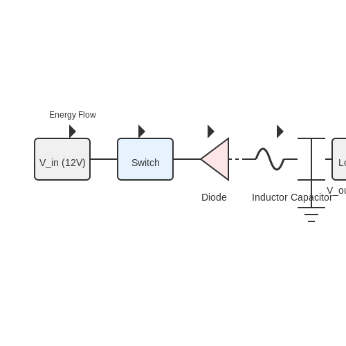
In practical applications, the integration of these components into a single circuit enables the conversion of higher input voltages to lower output levels efficiently. Real-world applications of Buck Converters can be found in power management systems for integrated circuits, battery-powered devices, and renewable energy systems, showcasing their versatility and importance in modern electronics. To visualize these interactions, a block diagram indicating the flow of energy through the Buck Converter, showing the interaction of the switch, diode, inductor, and capacitor, would provide clarity. Such diagrams serve as valuable references for engineers designing system architectures. By understanding these components and their functions, engineers and researchers can effectively design and optimize Buck Converters tailored for specific applications, leveraging their efficiency and adaptability to meet the demands of contemporary electronic systems.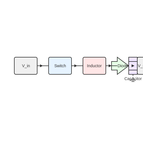
2. Schematic Diagram
2.1 Schematic Diagram
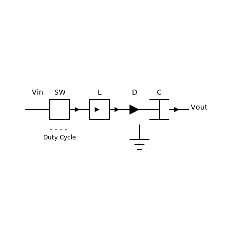
In the realm of power electronics, the buck converter stands out as a pivotal component for converting a higher input voltage to a lower output voltage with high efficiency. Understanding the operation and design of a buck converter requires a firm grasp of its schematic diagram, which serves as both a blueprint and a functional representation of the circuit. The schematic diagram of a buck converter typically comprises several essential elements: a high-side switch (usually a MOSFET), a low-side switch (often a diode or synchronous MOSFET), an inductor, a capacitor for smoothing output voltage, and feedback components which are integral for maintaining the desired output voltage. To elucidate this further, we can dissect each element and its functionality as follows:- High-Side Switch: This component is responsible for connecting the input voltage to the inductor. In most configurations, a MOSFET is utilized because of its efficiency and fast switching capabilities.
- Inductor: This component stores energy when the switch is on and releases it when the switch is off, effectively smoothing the current delivered to the output.
- Diode (or Synchronous Switch): The diode provides a path for the current when the high-side switch is off, ensuring that the output voltage remains stable during the switching period.
- Capacitor: This element filters the voltage across the output, reducing voltage ripple and ensuring a steadier output.
- Feedback Loop: The feedback components generally include resistors and an operational amplifier, which sense the output voltage and adjust the duty cycle of the switch to maintain a constant output voltage.
2.2 Choosing Components
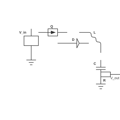
In designing a buck converter, one of the most crucial phases is the thoughtful selection of components, which directly impacts the performance, efficiency, and overall reliability of the circuit. Each component plays a role that must align precisely with the specified requirements of the application. Therefore, it is essential to understand the characteristics and parameters governing each part of the buck converter.Inductor Selection
The inductor is pivotal in energy storage and transfer within the buck converter. To select the appropriate inductor, consider the following parameters:- Inductance Value (L): The inductance must be chosen to maintain continuous conduction mode under all load conditions. The required inductance can be approximated using the formula:
$$ L = \frac{(V_{out} \cdot (V_{in} - V_{out}))}{f_{sw} \cdot I_{out} \cdot V_{in}} $$This equation ensures that the inductor can handle the required changes in current without saturating.
- Current Rating: Select an inductor with a saturation current rating above the peak inductor current, which is key to avoiding performance loss due to saturation.
- DC Resistance (DCR): A lower DCR is vital as it reduces conduction losses, contributing to overall efficiency.
Capacitor Selection
Capacitors in buck converters are mainly used for output voltage smoothing and transient response improvement. It is critical to understand different types of capacitors—ceramic, electrolytic, and tantalum each has distinct properties.- Capacitance Value (C): The required capacitance depends on the acceptable output ripple voltage and can be calculated using:
$$ C = \frac{I_{out} \cdot D}{\Delta V_{out} \cdot f_{sw}} $$where \(D\) is the duty cycle and \(\Delta V_{out}\) is the maximum allowable voltage ripple. This equation indicates how capacitance influences the output stability and response speed.
- Voltage Rating: The capacitor’s voltage rating must exceed the maximum output voltage, factoring in possible voltage spikes.
- Equivalent Series Resistance (ESR): Lower ESR improves efficiency by minimizing losses, thus enhancing thermal management.
Switch Selection
The power switch in a buck converter is fundamental for controlling energy flow. Commonly, MOSFETs (metal-oxide-semiconductor field-effect transistors) are used due to their efficacy.- Voltage Rating: The MOSFET’s drain-source voltage rating should surpass the maximum input voltage to account for transients.
- Current Rating: Adequately rated for peak current conditions, considering both continuous and pulsed operation scenarios.
- RDS(on): The lower the on-resistance, the lesser the power loss during operation; hence, selecting a MOSFET with low RDS(on) improves efficiency.
- Gate Charge (Qg): A lower gate charge reduces switching losses and enhances the overall operating frequency.
Diode Selection
The diode’s role in a buck converter is to provide a path for inductor current when the switch is off. Schottky diodes are commonly preferred due to their fast switching speeds and low forward voltage drop.- Voltage Rating: The reverse voltage rating of the diode must exceed the maximum output voltage.
- Current Rating: Similar to the switch, the diode should handle peak currents, ensuring reliability.
- Forward Voltage Drop (VF): A lower VF minimizes power loss during conduction, thus increasing efficiency.
2.3 Layout Considerations
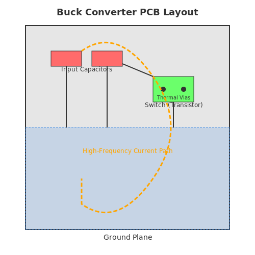
The design of a buck converter is not merely a task of selecting the right components and connecting them; it requires careful consideration of the layout of those components on the printed circuit board (PCB). The integrity of the buck converter's performance heavily relies on effective management of parasitic elements, thermal management, and overall electromagnetic interference (EMI) issues.
Understanding Parasitics
In any practical circuit, parasitic elements—such as inductance and capacitance resulting from traces and component leads—can significantly impact performance. For instance, the layout of the input and output capacitors in a buck converter is crucial. If positioned too far from the switching node, the inductance can lead to voltage overshoot and ringing, thereby deteriorating voltage regulation and switching performance.
For optimal performance, it is essential to minimize the loop area associated with the high-frequency signals and current paths. This can be achieved through a proper arrangement of the power stage components. Generally, the layout should follow these key practices:
- Place the input capacitors close to the switch (transistor). This minimizes the loop area for high-frequency current, thereby reducing the inductance and improving dynamic response.
- Use wide traces. To accommodate high currents without significant voltage drops, wider traces are essential; they also help reduce resistive losses.
- Short, direct connections. Wherever possible, ensure direct paths between components to minimize parasitic inductance.
Thermal Management
Another important aspect of layout considerations is thermal management. Buck converters convert higher voltage to lower voltage through switching, which generates heat due to switching losses and conduction losses. Implementing adequate thermal relief is essential to prevent component failure.
Here are some strategies to enhance thermal performance:
- Thermal vias. Use thermal vias to connect component pads to copper planes beneath the PCB, which can help dissipate heat effectively.
- Copper pour. Implementing a copper pour connected to ground or a power plane can aid in distributing heat away from critical components.
- Component placement. Keep heat-generating components away from temperature-sensitive ones.
Electromagnetic Interference (EMI) Control
EMI is a significant concern in switching power supplies due to rapid switching of currents. Proper layout strategies can significantly mitigate EMI issues:
- Ground planes. A solid ground plane helps to reduce radiated emissions and provides a return path for return currents, which is beneficial for both signal integrity and EMI performance.
- Keep noisy components away from sensitive circuits. Positioning high-frequency components far from sensitive analog circuits minimizes the risk of crossover interference.
- Use shields and barriers. Implementing physical barriers can further safeguard against noise pickup.
In conclusion, meticulous layout considerations in the design of buck converters are essential for achieving optimal efficiency, thermal stability, and minimal electromagnetic interference. By giving due attention to these factors, engineers can enhance the performance and reliability of buck converters in their applications, which range from powering portable devices to industrial automation systems.
3. Efficiency
3.1 Efficiency
In modern electrical systems, the efficiency of a buck converter is paramount, not only for performance optimization but also for thermal management and sustainability. As power considerations have risen in relevance due to environmental constraints, understanding the efficiency metrics of a buck converter is critical for their application in real-world systems, particularly in battery-operated devices and renewable energy setups. The efficiency of a buck converter is generally defined by the ratio of the output power \( P_{out} \) to the input power \( P_{in} \):Power Loss Mechanisms
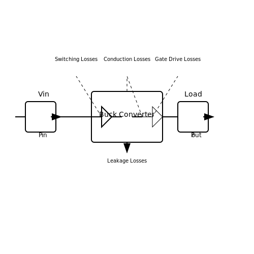
To critically analyze the efficiency, we must delve into the factors that contribute to power losses:- Conduction Losses: These occur when current flows through the MOSFET switches and diodes. The most significant contributors are the on-resistance of the MOSFETs and the forward voltage drop across the diode.
- Switching Losses: Associated with the transitions of the MOSFETs — particularly when they switch on and off. These losses are influenced by the switching frequency and the rate of voltage change.
- Gate Drive Losses: The energy expended in charging and discharging the gate capacitance of the switching MOSFETs competes with the primary switching and conduction losses.
- Leakage Losses: These are losses that occur during the off state of the MOSFETs. They can be attributed to the leakage current flowing through the devices and the parasitic components of the system.
Efficiency Calculation
Calculating the efficiency of a buck converter necessitates an assessment of both the input and output properties, as well as the aforementioned losses. Let's say a buck converter outputs 5V at 2A (providing \( P_{out} = 10W \)) and the input voltage is 12V while drawing 1.2A (so \( P_{in} = 14.4W \)). The efficiency \( \eta \) can be calculated as follows: 1. Determine \( P_{out} \):Practical Relevance and Optimization Techniques
In practical applications, the efficiency of a buck converter has significant implications. A higher efficiency results in reduced heat generation, less need for heatsinking, and lower energy consumption, making it crucial in portable electronics, electric vehicles, and renewable energy systems. To enhance buck converter efficiencies, engineers may employ several optimization techniques, such as:- Use of synchronous rectification: This replaces diodes with low-Rds(on) MOSFETs to reduce conduction losses.
- High-frequency operation: Utilizing higher switching frequencies can lead to smaller components; however, this can also increase switching losses, thus necessitating a careful assessment.
- Advanced control strategies: Techniques such as adaptive voltage scaling can optimize performance dynamically based on load conditions.
3.2 Voltage Regulation
Voltage regulation in a buck converter is crucial for maintaining a stable output voltage despite variations in input voltage and load conditions. The essence of voltage regulation lies in the converter's ability to adjust its output dynamically, ensuring that the desired voltage level is consistently achieved, which is particularly important in sensitive electronic applications.
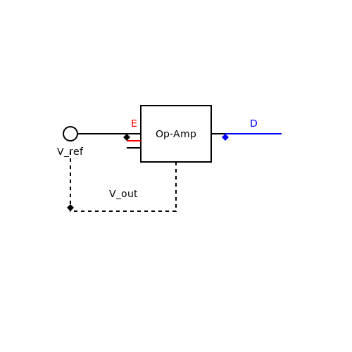
A common approach to achieve voltage regulation in buck converters is through the implementation of closed-loop feedback control. This technique utilizes an error amplifier to compare the output voltage with a reference voltage. Any deviation is used to adjust the duty cycle of the switching element, thereby modifying the output voltage accordingly. A typical feedback loop can be visualized as follows:
- Reference Voltage ($${V_{ref}}$$): The desired output voltage level.
- Output Voltage ($${V_{out}}$$): The actual voltage produced by the buck converter.
- Error Signal ($${E}$$): The difference between $${V_{ref}}$$ and $${V_{out}}$$.
- Duty Cycle ($${D}$$): The ratio of the on-time to the total time period of the switching cycle, which is varied to control the output voltage.
To derive the relationship between the duty cycle and the output voltage, let’s consider the basic operation of the buck converter. The output voltage can be expressed as:
Where:
- $${V_{out}}$$ is the output voltage,
- $${D}$$ is the duty cycle (0 < $${D} < 1$$), and
- $${V_{in}}$$ is the input voltage.
From this equation, one can see that by adjusting the duty cycle $${D}$$, the output voltage $${V_{out}}$$ can be regulated. For instance, if the input voltage increases, reducing the duty cycle will maintain the output voltage within the desired range.
Next, let's explore the operation of a typical feedback control loop in more detail. The operational amplifier (op-amp) forms the core of the voltage control loop. Its configuration can either be integrating or proportional. An important consideration is the stability of the system, particularly how the loop responds to changes in load and input voltage. If the system is too responsive, it may oscillate; if it is too sluggish, it may not effectively maintain regulation.
Practical Implementation and Stability Considerations
In practice, several techniques can enhance voltage regulation:
- Compensation Networks: Adding compensating networks (such as lead, lag, or PID controllers) can improve system stability and response time.
- Capacitance Selection: Choosing the appropriate capacitance at the output affects the transient response and stability. Larger capacitors can help reduce voltage fluctuations during load changes.
- Inductor Selection: Inductor value affects ripple current and time constant of the filter, thus influencing voltage regulation performance.
Real-world applications of buck converters are abundant, spanning from power supplies for computers and smartphones to electric vehicle chargers. In these implementations, maintaining a stable voltage is critical not only for the functionality of the device but also for extending the lifespan of sensitive components.
In summary, voltage regulation in buck converters is an intricate balance of design, control mechanisms, and component selection. As technology advances, innovations in control algorithms and circuitry continue to improve the efficiency and reliability of voltage regulation techniques, making them indispensable in modern electronics.
3.3 Load Transient Response
The load transient response of a buck converter is a critical aspect of its performance, particularly in applications requiring rapid changes in load conditions. Understanding how a buck converter reacts to sudden variations in load can optimize circuit design in power management systems used in portable electronics, automotive applications, and renewable energy systems. At the heart of the buck converter's operation is its ability to regulate output voltage despite fluctuations in the load current. When the load on the converter changes abruptly, the energy demand on the output also changes, which creates a dynamic scenario that the control system must manage effectively. This dynamic behavior can be analyzed in terms of voltage overshoot, undershoot, settling time, and the root cause of oscillations.Transitional Events in Buck Converters
When a load transient occurs, such as suddenly switching from a light load to a heavy load, two primary events take place: 1. Energy Demand Change: A sudden increase in load current causes the output voltage to drop, as the energy supplied by the buck converter temporarily falls short of the load demand. 2. Control Loop Response: The control loop (typically via a feedback mechanism) reacts to this change in output voltage by adjusting the duty cycle of the pulse-width modulation (PWM) signal to increase the energy delivered from the input to the output. In practical terms, this means that the output voltage of the buck converter can briefly sag below its nominal value before the control system compensates by delivering more energy, achieving equilibrium. This has real-world implications; for instance, in sensitive electronic circuits, maintaining voltage within strict limits is vital to prevent malfunction or shutdown.Mathematical Modeling of Load Transients
To quantitatively analyze the response of a buck converter to load transients, we can apply the principles of linear control theory. We start by defining a few critical parameters: - L: Inductance in the output stage. - C: Capacitance at the output. - R: Load resistance. - V_out: Desired output voltage. - V_load: The voltage across the load during transient. The transfer function for the system can be represented as: $$ H(s) = \frac{V_{out}(s)}{V_{load}(s)} = \frac{1}{LCs^2 + \frac{1}{R}s + 1} $$ This second-order transfer function indicates that the system has a damping factor and a natural frequency that depends on the inductor and capacitor values. The response can be analyzed using the Laplace transform, which allows us to consider the transitioning from steady-state operation to the transient state. To derive expressions for overshoot and settling time, we can analyze the poles of the transfer function. Consider that for a critically damped response: $$ \text{Settling Time (Ts)} \approx \frac{4}{\zeta \omega_n} $$ where \(\zeta\) represents the damping ratio and \(\omega_n\) is the natural frequency of the system. Example Calculation If we assume an output inductor \(L = 10 \, \mu H\), output capacitor \(C = 100 \, \mu F\), and a load resistance of \(R = 10 \, \Omega\), we can calculate the natural frequency:Real-World Considerations
In actual circuit applications, the performance of the buck converter's transient response is subject to many factors, including: - PCB Layout: Poor layout can introduce parasitic inductance and capacitance that hinder dynamic response. - Component Selection: The choice of inductors and capacitors affects both the speed of response and maximum load current the converter can handle. - Feedback Loop Design: Advanced control techniques, such as voltage-mode and current-mode control, can significantly enhance transient response and stability. Ultimately, understanding load transient response in buck converters equips engineers and researchers to design more robust power supplies, reducing the risk of operational failures and improving system performance in increasingly demanding applications.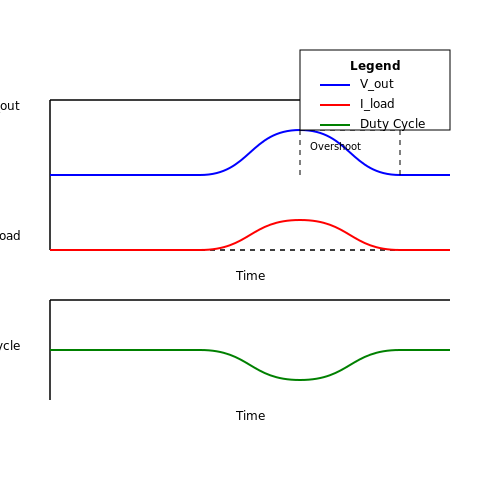
4. Power Management in Electronics
4.1 Power Management in Electronics
Power management is a fundamental aspect of modern electronics that dictates the efficiency, performance, and reliability of electronic systems. In a world where energy conservation and efficiency are paramount, power management circuits—such as buck converters—play a pivotal role in regulating the voltage delivered to microcontrollers, sensors, and other digital devices.
A buck converter, specifically, is a type of DC-DC converter designed to step down voltage with high efficiency. It achieves this through the use of switching elements, inductors, and capacitors, harnessing the principles of energy storage and transfer. Understanding the mechanics of a buck converter begins with grasping the concept of duty cycle and its influence over output voltage. The duty cycle, defined as the ratio of the time the switch is on to the total period of the switching cycle, directly affects the average voltage presented to the load.
Understanding the Buck Converter
To derive the output voltage of a buck converter, we can relate it to the input voltage ($$V_{in}$$) and the duty cycle ($$D$$) using the following formula:
This relation highlights how by appropriately adjusting the duty cycle, one can control the output voltage, which is crucial for devices requiring lower operational voltages than their power supply.
Efficiency Considerations
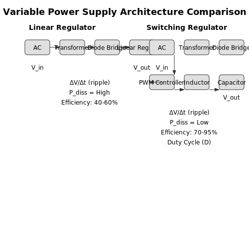
In the context of power management, efficiency is a critical concern, especially in battery-operated devices where every milliampere counts. A well-designed buck converter can achieve an efficiency of over 90%, significantly minimizing energy loss typically found in linear regulators. The efficiency ($$\eta$$) of a buck converter can be calculated as:
Where $$P_{out}$$ is the output power and $$P_{in}$$ is the input power. This efficiency can, however, be influenced by various factors such as switching losses, inductor core losses, and even conduction losses in the feedback path.
Applications of Buck Converters
Buck converters are ubiquitous in electronic devices ranging from personal electronic gadgets to more complex applications such as electric vehicles and renewable energy systems. By maintaining efficient power conversion rates, these devices can prolong battery life and enhance performance across various operating conditions.
For instance, in portable electronics like smartphones or wearables, buck converters enable the step-down of battery voltage to properly power low-voltage integrated circuits while maintaining thermal management. The switch-mode nature of buck converters allows designers to maintain a compact circuit size, which is crucial in today’s trend towards miniaturization.
Real-World Case Study: Power Management in Telecommunications
In telecommunications, the efficiency of power management solutions becomes critical due to continuous operational demands. A case study involving a major telecommunications provider shows the improvement in power consumption achieved through implementing buck converters for powering base stations. By replacing outdated linear voltage regulators with buck converters, the provider noted a reduction in energy use by over 25%, translating to significant cost savings and reduced environmental impact.
In conclusion, as systems evolve and demands for efficiency continue to grow, understanding the role of buck converters in power management will remain essential for engineers and designers alike. Balancing between performance, size, and efficiency will lead to smarter, more sustainable electronic designs in the future.
4.2 Renewable Energy Systems
The integration of buck converters in renewable energy systems marks a significant enhancement in the efficiency and functionality of energy management. A buck converter, also known as a step-down converter, is essential for applications that require a lower output voltage from a higher input voltage, thus enabling effective energy use in decentralized power generation and storage solutions.
In renewable energy applications, such as solar power systems or wind turbines, buck converters can be utilized to manage the energy harvested efficiently. The unpredictable nature of renewable energy sources necessitates robust power management strategies to ensure that the energy can be redirected appropriately for storage or immediate use. By harnessing the capabilities of buck converters, one can optimize the overall system performance while minimizing losses during the energy conversion process.
Operational Principles of Buck Converters in Renewable Energy
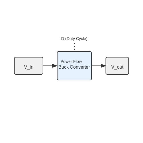
To understand the operational principles of buck converters, consider the fundamental relationship that governs the input-output voltage conversion, defined by the duty cycle. The duty cycle (D) is the fraction of time that the switch is closed within a switching period, which determines the efficiency of the voltage conversion.
The output voltage (Vout) for a buck converter can be mathematically expressed as:
where Vin is the input voltage. The design of the converter must include compensatory mechanisms for voltage regulation to adapt to variations in the input voltage from renewable sources, which can fluctuate due to environmental conditions.
Efficiency and Loss Considerations
A critical aspect of employing buck converters in renewable energy systems is their efficiency, which can be influenced by several factors, including:
- Conduction losses: Occur due to resistance in the inductor and switches.
- Switching losses: Related to the rapid on-and-off transitions of the switch.
- Capacitive losses: Result from the charging and discharging of output capacitors.
Optimizing these factors is crucial for the effective application of buck converters in renewable energy contexts, particularly where efficiency directly correlates with the overall energy yield of solar panels or wind turbines. One notable enhancement in technology is the use of synchronous rectification, which replaces the traditional diode with a switch, significantly reducing these losses.
Real-World Applications and Case Studies
Numerous case studies illustrate the effectiveness of buck converters in renewable systems. For instance, in solar photovoltaic systems, buck converters control the connection between solar panels and storage batteries. Their ability to efficiently manage power flows not only improves battery life by preventing overcharging but also maximizes the energy harvested from the panels.
In wind energy applications, buck converters are integrated to regulate the voltage output from variable speed turbines, ensuring consistent power delivery to the grid or local loads. Such implementations validate the practical relevance of these converters in modern sustainable energy infrastructures.
Future advancements in buck converter technology, particularly when integrated with digital control strategies and energy storage solutions, are likely to enhance their role in powering advanced renewable energy systems, paving the way for innovative energy management practices in the transition towards a sustainable energy future.
4.3 Automotive Applications
In recent years, the automotive sector has placed an increasing emphasis on the integration of energy-efficient systems, largely driven by decarbonization efforts and the shift towards electric vehicles (EVs). At the heart of many of these systems lies the buck converter—an indispensable power electronics component that converts higher voltage levels to lower ones efficiently. This subsection explores how buck converters are utilized in automotive applications, providing insights into their design considerations, functionality, and the essential role they play in modern vehicles.Power Management in Electric Vehicles
As electric vehicles gain prominence, power management is critical for optimizing battery usage and extending driving range. Buck converters are employed to step down voltages from the high-voltage battery packs, typically ranging from 300V to 800V, to suitable levels for various vehicle components such as electronic control units (ECUs), motors, and lighting systems. The operation of a buck converter is predicated on its ability to effectively manage the input voltage. The device switches between conductance and non-conductance states, storing energy in an inductor during the on-state and releasing it to the output in the off-state. This method considerably reduces energy losses compared to linear regulators, enhancing overall vehicle efficiency.Regenerative Braking Systems
A particularly noteworthy application of buck converters in vehicles is in regenerative braking systems. When a vehicle decelerates, energy that would traditionally be lost as heat in friction brakes can be harvested and redirected to recharge the vehicle's battery. In this scenario, the buck converter plays a crucial role by stepping down the voltage from the system during the energy recovery phase. When the vehicle brakes, the electric motor operates in reverse, acting as a generator. The generated voltage is often higher than what the battery can safely accept. The buck converter regulates this voltage, ensuring safe and efficient energy transfer back to the battery.Load Regulation and Thermal Management
Another important consideration in automotive applications is load regulation and thermal management. Buck converters must be designed to handle varying load conditions while maintaining constant output voltage. The implementation of feedback mechanisms within the buck converter enhances its response to load changes, ensuring stability under different operational scenarios. Moreover, thermal management is paramount in automotive design, as components are subjected to fluctuating temperatures and must operate reliably over a wide range of conditions. Advanced thermal management solutions for buck converters may include the use of heat sinks, thermal pads, and strategic placement of components within the vehicle to optimize airflow and reduce thermal resistance.Future Trends and Challenges
The evolution of automotive applications continues to drive innovations in buck converter designs. As manufacturers strive towards increasingly compact and lightweight components, the integration of advanced materials such as silicon carbide (SiC) and gallium nitride (GaN) in buck converters is gaining traction. These materials enable higher switching frequencies, greater efficiency, and a reduction in thermal losses, making them ideal for modern EVs. However, challenges remain, including electromagnetic interference (EMI) and increased complexity in the control circuitry. Addressing these issues is critical as the automotive industry embraces more sustainable and efficient technologies. In summary, the buck converter's role within automotive applications is fundamental, enabling energy efficiency and enhanced performance in both traditional and electric vehicles. As the industry continues to advance, the buck converter is likely to remain at the forefront of power management solutions.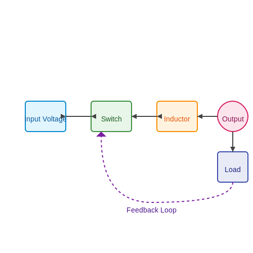
5. Common Issues and Solutions
5.1 Common Issues and Solutions
Buck converters are versatile and widely used in power management applications, but like any electronic device, they are prone to certain issues. Understanding these challenges is crucial for engineers and researchers to enhance the reliability and performance of these converters. This section delves into some common issues encountered in buck converter design and operation, along with practical solutions.
Output Voltage Ripple
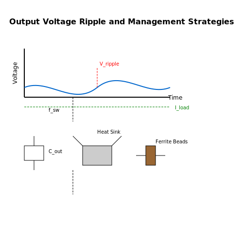
One of the primary issues in buck converters is output voltage ripple, which can adversely affect the performance of the load, especially in sensitive electronic circuits. The ripple voltage (\(V_{ripple}\)) is influenced by several factors, including switching frequency, inductor value, and output capacitor.
The equation for estimating output voltage ripple can be given by:
Where:
- Iload: Load current
- fsw: Switching frequency
- Cout: Output capacitance
To mitigate voltage ripple, consider using a capacitor with a larger value or employing low equivalent series resistance (ESR) capacitors, such as ceramic types, which can significantly reduce ripple.
Thermal Management
As buck converters operate, they generate heat due to conduction and switching losses. High temperatures can lead to decreased efficiency and potential damage. The challenge lies in maintaining optimal thermal performance while ensuring compact design.
Effective heat sinking and proper ventilation are essential strategies for thermal management. Additionally, selecting components with higher thermal capabilities can alleviate excess heat buildup. In some designs, implementing synchronous rectification—using MOSFETs instead of diodes—can also reduce conduction losses and improve thermal performance.
Electromagnetic Interference (EMI)
Due to the high switching frequencies in buck converters, EMI poses another significant concern. It can disrupt nearby electronic devices or degrade the performance of the converter itself. The rapid switching can lead to voltage spikes and noise in the power supply lines.
To address EMI, consider incorporating proper PCB layout strategies. This includes minimizing loop areas by placing components close together and using twisted pairs for signal paths. Additionally, the use of ferrite beads on the input and output lines can help suppress high-frequency noise effectively.
Control Loop Stability
Control loop stability is crucial for maintaining the desired output voltage under varying load conditions. A poorly designed feedback loop can result in oscillations or sluggish response to load changes. Analyzing the phase margin and gain margin can provide insights into system stability.
Utilizing a compensator in the feedback loop can significantly enhance stability. For example, employing Type II or Type III compensation networks can provide necessary phase lead to ensure stable operation across different load conditions.
Component Tolerances and Derating
Component tolerances can lead to discrepancies in performance during operation. Variations in inductor value, capacitor ESR, and switching frequencies can affect output voltage regulation and efficiency. Therefore, component derating—operating components below their maximum ratings—can enhance reliability.
For instance, selecting inductors with higher current ratings than expected load currents can avoid saturation, ensuring steady performance. Similarly, utilizing capacitors rated for voltages significantly above the converter's maximum output voltage adds a safety margin against voltage spikes.
Real-World Applications and Conclusion
In real-world applications, understanding and addressing these common issues can significantly enhance the performance and reliability of buck converters. Whether implemented in portable electronics, automotive applications, or industrial equipment, resolving these challenges allows engineers to leverage buck converters more effectively, ensuring optimal operation.
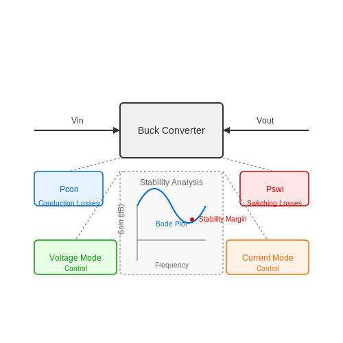
5.2 Performance Tuning
The performance of a buck converter—one of the most vital components in the realm of power electronics—depends on various factors ranging from its design to component selection and control strategies. In this section, we will explore the nuanced aspects of performance tuning that enhance the efficiency, transient response, and stability of a buck converter. Understanding these factors is essential for engineers and researchers aiming to optimize converter designs for specific applications.
Understanding Efficiency and Power Losses
The efficiency of a buck converter is its ability to convert input power to output power effectively. It can be mathematically expressed as:
Where \( P_{out} \) is the output power and \( P_{in} \) is the input power. To maximize efficiency, one must analyze several components: conduction losses, switching losses, and gate drive losses.
Conduction losses are primarily due to the on-resistance in the MOSFETs and the resistance in inductors and capacitors. The average conduction loss for a MOSFET can be modeled as:Where \( I_{out} \) corresponds to the output current and \( R_{DS(on)} \) is the on-state resistance of the MOSFET.
Switching losses occur during the transitions between the on and off states of the transistor. These losses are often dependent on the switching frequency and can be modeled as:
Here, \( t_{on} \) and \( t_{off} \) represent the turn-on and turn-off times, respectively, and \( f_{sw} \) is the switching frequency.
Transient Response Optimization
Another crucial aspect of performance tuning is the transient response of the buck converter, which describes how quickly the output voltage can respond to sudden changes in load current or input voltage. To optimize transient response, one effective approach is to choose appropriate output capacitance and inductor values. Larger output capacitors can reduce voltage deviations during load transients.
However, one must be cautious: too high a capacitance may lead to a sluggish response due to increased time constants. Therefore, the selection can be guided by the Root Locus or Bode plot techniques, which can illustrate the impact of varying these components on the overall system stability.
Feedback Control Strategies
A versatile control strategy is essential for achieving stable and efficient operation of buck converters. The most commonly employed methods include voltage mode and current mode control schemes. Voltage mode control provides simplicity and ease of design but may struggle with power supply rejection in noisy environments. In contrast, current mode control offers better transient response and inherent overcurrent protection, albeit with increased complexity.
The design of a feedback loop often relies on compensating the system to achieve desired performance. This compensation can be achieved using phase lead or lag techniques to ensure adequate phase margins, facilitating stability throughout the operational range.
Real-World Applications and Case Studies
Real-world implementations of performance tuning have led to significant improvements in consumer electronics, electric vehicles, and renewable energy systems. For instance, adjusting control parameters in automotive applications has resulted in better fuel efficiency and longer battery life. Similarly, in photovoltaic systems, optimized buck converters help to achieve maximum power point tracking (MPPT) under varying lighting conditions.
In conclusion, performance tuning of a buck converter is not merely a theoretical endeavor but a practical necessity that requires a nuanced understanding of the underlying principles. By refining design parameters and control mechanisms, one can tailor the operational characteristics of buck converters for specific applications, ultimately driving innovation in various fields of engineering.
5.3 Safety Considerations
As we delve into the intricacies of buck converters, it becomes imperative to address the safety considerations associated with their implementation. While these devices are celebrated for their efficiency in DC-DC conversion, they also present potential hazards that must be managed effectively to ensure reliability and longevity. Understanding these risks not only protects the device but also safeguards personnel and associated circuitry.Electromagnetic Interference (EMI)
One of the foremost safety concerns associated with buck converters is electromagnetic interference (EMI). The rapid switching of the transistors in a buck converter generates high-frequency harmonics, which can radiate and disrupt nearby electronic devices. This interference can lead to malfunctions in sensitive equipment, affecting performance and reliability. To mitigate EMI, engineers should employ techniques such as:- Proper PCB layout: Keeping high-frequency paths short and ensuring a solid ground plane can help reduce EMI generation.
- Use of filtering components: Adding inductors and capacitors at the input and output can suppress high-frequency noise.
- Shielding: Encasing the buck converter within a grounded shield can further contain EMI emissions.
Thermal Management
Another critical safety consideration is thermal management. Buck converters inherently generate heat due to power losses during operation, primarily in the switching elements (e.g., MOSFETs) and passive components (e.g., inductors and capacitors). Excessive heat can lead to component failure, reduced efficiency, and even catastrophic events such as fires. To ensure effective thermal management, consider the following approaches:- Use of heat sinks: Attaching heat sinks to high-power components can dissipate heat more effectively.
- Active cooling solutions: Implementing fans or liquid cooling systems in high-power applications can maintain operating temperatures within safe limits.
- Thermal pads or thermal paste: These can enhance thermal conduction between components and heat sinks, improving heat dissipation efficiency.
Voltage and Current Limitations
Buck converters are rated for specific voltage and current limits, and exceeding these parameters can result in significant safety risks. For example, overcurrent can cause MOSFETs to enter thermal runaway, potentially leading to component damage or failure. To prevent overvoltage and overcurrent conditions, engineers should:- Incorporate protection circuits: Use fuse elements, circuit breakers, or current-limiting features to prevent excessive current draw.
- Design for a conservative operating range: Ensure that the device operates well within its specified limits during normal conditions and transient situations.
- Runtime monitoring: Implement feedback mechanisms that can adjust output or shut down the converter when parameters exceed safe values.
Isolation Techniques
In applications where safety is paramount (e.g., automotive and medical devices), it is essential to consider isolation techniques. Isolation methodologies include the use of opto-isolators and transformers to separate user-accessible circuitry from high-voltage components. This adds a layer of protection against electric shock and can also shield sensitive components from noise and transients. Additionally, proper grounding practices must be adhered to in order to minimize the risk of ground loops and ensure safe operation. It is critical to incorporate these practices into the design phase rather than as an afterthought.Conclusion
In summary, while buck converters are vital components in power electronics, their safe operation necessitates careful consideration of EMI, thermal management, voltage and current limitations, and isolation techniques. By adhering to these safety measures, engineers can develop robust systems that not only function efficiently but also ensure the well-being of users and the integrity of surrounding devices. Integrating safety into the design process ultimately leads to enhanced reliability and performance in the field.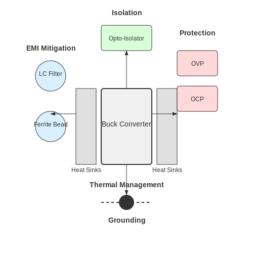
6. Synchronous Buck Converters
6.1 Synchronous Buck Converters
Synchronous buck converters are an evolution of the traditional buck converter topology, prominently characterized by their use of synchronous rectification. This approach improves efficiency, particularly in low-voltage applications where conventional diode rectification can present significant losses. By integrating active switching elements in place of diodes, synchronous buck converters optimize performance and cater to the demands of modern electronic systems.
Fundamental Principle of Synchronous Buck Converters
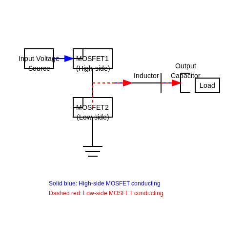
The key distinction in synchronous buck converters lies in their configuration of two switches: a high-side switch (usually an N-channel MOSFET) and a low-side switch (also typically an N-channel MOSFET). This arrangement allows for bidirectional current flow, enabling lower conduction losses compared to diode-based systems.
To grasp the operational efficiency of synchronous converters, it's important to understand how they transition between the on and off states of these switches. During the on state of the high-side switch, the inductor is charged, while the low-side switch remains off, resulting in energy storage within the inductor. Conversely, when the high-side switch turns off, the low-side switch turns on to provide a path for the inductor current, effectively transferring energy to the output capacitor and the load.
Efficiency Calculation
Efficiency (η) is a critical metric in evaluating a synchronous buck converter's performance. It can be determined using the formula:
Where:
- Pout is the output power delivered to the load.
- Pin is the input power supplied by the input voltage source.
In synchronous operation, the primary losses include conduction losses across the MOSFETs and the switching losses associated with rapid state transitions. The use of low RDS(on) MOSFETs in conjunction with techniques like adaptive gate drive optimization can further mitigate conduction losses, driving efficiency upwards and facilitating higher current demands.
Control Methods for Synchronous Buck Converters
Effective control mechanisms are essential for regulating the output voltage of synchronous buck converters, as they influence the dynamic response and stability of the converter. Two prevalent methodologies include voltage mode control (VMC) and current mode control (CMC).
- Voltage Mode Control: This methodology operates primarily on the output voltage, comparing it to a reference voltage to maintain a desired output.
- Current Mode Control: This approach includes current feedback in its control loop, allowing faster response to sudden load changes by limiting the inductor current.
Each control strategy has its unique advantage. CMC, for instance, not only enhances transient response but also provides inherent short-circuit protection through current limiting, thus proving advantageous for safety-critical applications.
Application Domains of Synchronous Buck Converters
The practical utility of synchronous buck converters extends across various domains, particularly in high-efficiency power delivery systems. They are widely utilized in:
- DC-DC converters for battery-powered devices: Used in smartphones, laptops, and power tools to optimize battery life and performance.
- Automotive Applications: Dedicated to supplying power to advanced driver-assistance systems (ADAS) and other electronic subsystems.
- Data Centers: Employed for delivering highly efficient power to servers and networking equipment, where efficiency relates directly to operating costs.
These applications highlight the importance of continuous innovation in buck converter designs, paving the way for more compact, efficient, and reliable power management solutions.
6.2 Digital Control Methods
In the realm of switching power supplies, particularly in the operation of buck converters, digital control methods have emerged as a revolutionary approach to enhance performance and reliability. Unlike analog control methods, which predominantly rely on continuous variable signals, digital control incorporates discrete-time signals, allowing for greater precision and flexibility in managing converter dynamics. The implementation of digital control in buck converters can be fundamentally linked to advancements in microcontroller and digital signal processor technologies. These devices enable the use of sophisticated algorithms and techniques to optimize control loops, such as PID (Proportional, Integral, Derivative) control and model predictive control.The PID Controller in Digital Systems
The PID controller is one of the most widely used control algorithms in both analog and digital systems. It operates by calculating an error value as the difference between a desired setpoint and a measured process variable. In the context of a buck converter, the setpoint could be the output voltage, while the process variable is the actual output voltage. To transition from analog to digital control, we can discretize the classic PID control laws. The PID controller can be represented as: $$ u[n] = K_p e[n] + K_i \sum_{k=0}^{n} e[k] + K_d (e[n] - e[n-1]) $$ where: - \( u[n] \) is the control signal, - \( e[n] \) is the error signal at time \( n \), - \( K_p \), \( K_i \), and \( K_d \) are the proportional, integral, and derivative gains, respectively. To implement this control scheme, the following steps are essential: 1. Sample the Output: The output voltage of the buck converter is continuously monitored using an analog-to-digital converter (ADC). 2. Calculate the Error: The difference between the setpoint and the actual output is computed at each sampling instant. 3. Update Controller: The discrete updates to the control signal \( u[n] \) are calculated using the PID formula. 4. Output Adjustment: The computed control signal is translated into PWM (Pulse Width Modulation) duty cycle adjustments that control the switching transistors in the buck converter. The transition from analog to digital control can introduce complexities such as quantization errors, latency, and potential instability. Thus, it is essential to employ strategies like anti-windup techniques in case of saturation, which helps maintain controller stability.Model Predictive Control: A Modern Approach
Another significant advancement in the field of digital control is the implementation of model predictive control (MPC) for buck converters. Unlike traditional PID controllers, MPC utilizes a system model to predict future outputs based on current states and control actions. This approach involves more computational effort but offers numerous advantages, including: - Multi-variable control: MPC can optimize multiple outputs simultaneously while respecting constraints. - Forward-looking control: By predicting future states, it can anticipate disturbances and adjust outputs preemptively. Implementing MPC involves the following key steps: 1. Modeling: Develop a mathematical model of the buck converter, typically achieved through state-space representation. 2. Optimization: At every control step, solve an optimization problem to minimize a cost function that accounts for deviations from the setpoint and controls input energy. 3. Control Law Execution: Apply the first control action from the computed optimal sequence to the system, then repeat the process at the next time step. The equations governing the buck converter’s dynamics can be expressed using the state-space model: $$ \begin{bmatrix} x[n+1] \\ y[n] \end{bmatrix} = A \begin{bmatrix} x[n] \\ u[n] \end{bmatrix} + B \cdot d[n] $$ where: - \( x[n] \) represents the state variables (e.g., inductor current, capacitor voltage), - \( y[n] \) represents the output, - \( A \) is the state matrix, - \( B \) is the input matrix, - \( d[n] \) represents disturbances. MPC provides a robust framework for controlling buck converters under variable operating conditions, ensuring that performance remains optimal across a range of scenarios.Practical Applications of Digital Control in Buck Converters
The real-world implications of these digital control techniques are profound. Digital controllers offer the potential for improved efficiency, reliability, and design flexibility, making them ideal for various applications. Industries such as renewable energy systems, electric vehicles, and consumer electronics increasingly adopt buck converters controlled digitally due to their efficiency and adaptive capabilities. Furthermore, the integration of digital signal processing with advanced control strategies, such as fuzzy logic control or neural networks, may further enhance the performance of buck converters in the future, allowing for more intelligent and responsive power management solutions. In conclusion, the integration of digital control methods in buck converters signifies a crucial advancement in the power electronics landscape. By moving beyond traditional analog controls, these methods pave the way for more sophisticated, efficient, and adaptive power conversion systems capable of meeting the demands of modern technology.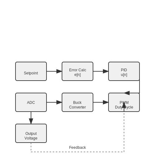
6.3 Future Trends in Power Conversion
The landscape of power conversion technology is continuously evolving, driven by demands for higher efficiency, smaller form factors, and enhanced functionality. Among these advances, buck converters play a pivotal role in various applications, from portable electronics to renewable energy systems. Here, we explore some of the most promising future trends in power conversion.
Integration of Advanced Materials
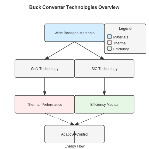
Recent developments in materials science have provided engineers with new opportunities to enhance the performance of buck converters. One significant trend is the use of wide bandgap (WBG) semiconductors, such as silicon carbide (SiC) and gallium nitride (GaN). These materials exhibit superior thermal performance, higher breakdown voltages, and faster switching speeds compared to conventional silicon semiconductors.
For instance, deploying GaN in buck converters can reduce conduction losses and increase efficiency, especially in high-frequency applications. As these materials become more commercially viable, we will likely see a broader adoption in consumer electronics, electric vehicles, and industrial power supplies.
Smart and Adaptive Power Conversion
Another noteworthy trend is the integration of intelligence into power conversion systems, leading to the emergence of smart and adaptive buck converters. These systems utilize advanced control algorithms and sensors to optimize performance based on real-time conditions.
Using feedback mechanisms, these converters can adjust their operating parameters, such as duty cycle and frequency, in response to varying load conditions. This adaptability not only enhances efficiency but also prolongs the lifespan of power supply systems by minimizing thermal stress and wear.
Wireless Power Transfer Technologies
As wireless power transfer (WPT) technology gains traction, efficient buck converters will be essential in enabling effective energy management within these systems. WPT employs electromagnetic fields to transfer energy, often necessitating precise voltage regulation. Emerging applications in consumer gadgets and electric vehicles demonstrate the necessity for compact, efficient buck converters capable of handling varying power requirements.
Future developments likely include innovations in resonant converter designs and improved electromagnetic coupling techniques that are compatible with buck conversion principles, ensuring that systems remain efficient across various load scenarios.
Energy Harvesting and Sustainability
The push for sustainability is leading to new applications for buck converters in energy harvesting technologies. Devices that capture energy from environmental sources—such as vibration, thermal gradients, and light—will require advanced power converters to regulate and store energy without wasting significant amounts.
Progress in this area could lead to the development of ultra-low power buck converters that can operate with minimal standby power, making green technologies more viable in everyday applications, including Internet of Things (IoT) devices.
Case Study: Electric Vehicles
The automotive industry, particularly electric vehicles (EVs), presents an excellent case study for the future trends in buck converters. EVs rely on power converters for efficient battery management and energy distribution. Innovations in buck converter technology, including higher integration levels and optimized thermal management, can significantly enhance the range and efficiency of electric vehicles.
As the market for EVs expands, companies are investing in advanced power conversion solutions. This investment not only reflects a commitment to electrification but also positions them to meet rigorous performance and efficiency standards.
In conclusion, the future of power conversion technology, particularly concerning buck converters, is shaped by advancements in material science, smart control systems, wireless technologies, and sustainability efforts. As these trends emerge, they promise to enhance the performance, efficiency, and applicability of power conversion systems across a wide range of industries.
7. Recommended Textbooks
7.1 Recommended Textbooks
- Power Electronics Handbook by Muhammad H. Rashid — This comprehensive guide serves as an in-depth exploration into power electronics, including the fundamentals, applications, and designs, with dedicated sections on various converter types, such as the buck converter.
- Power Electronics: Devices, Circuits, and Applications by Muhammad H. Rashid — This textbook offers an extensive introduction to the devices used in power electronics, covering essential concepts, including the operation of buck converters, supported by practical examples.
- Power Electronics Converter Harmonics by Chun T. Rim — Focuses on understanding harmonic generation in power converters, including buck converters, exploring both the theoretical aspects and practical methods to minimize or manage harmonics.
- Control of Power Electronic Converters by Frede Blaabjerg — This text explores control methods for power electronic converters, featuring chapters specifically on the control mechanisms utilized in buck converters and their applications in modern electronics.
- Power Electronics Basics: Operating Principles, Design, Formulas, and Applications by Yuriy Rozanov — Offers foundational principles of power electronics with practical insights into the design and application of converters like buck converters.
- Fundamentals of Power Electronics by Robert W. Erickson — An in-depth examination of power electronics, providing a solid foundation in converter design and analysis, including comprehensive coverage of linear and SWITCHED-MODE power supplies, featuring buck converters.
- The Essentials of Power Electronics by Andrzej M. Trzynadlowski — This book presents the essential circuits and design techniques for power electronics, encompassing detailed discussion and analysis of buck converters.
- Introduction to Power Electronics by Daniel W. Hart — A concise yet thorough introduction to power electronics, featuring practical applications and theoretical insights, including a detailed examination of buck converter operation and design.
- Electrical Power System Conversion by L.L. Freris — Examines the principles of electrical power conversion, with insights into the use and design of converters, such as buck converters, within power systems.
7.2 Online Resources
- Understanding Buck Power Stages in Switchmode Power Supplies by Texas Instruments — This comprehensive application note delves into the operation and design of buck converters, focusing on efficiency calculations, component selection, and output filtering. It is ideal for engineers looking to deepen their understanding of buck converter design.
- Basic Concepts of Linear Regulator and Switching Mode Power Supplies by Analog Devices — This tutorial provides a fundamental understanding of switching mode power supplies (SMPS) and highlights the differences between linear and switching regulators. It contains valuable insights for both practicing engineers and graduate students.
- Electronics Tutorials on Buck Converters — A detailed tutorial on buck converters, covering the basic operating principles, graphical derivations, and key performance indicators. Suitable for engineers and researchers needing an intuitive yet technical explanation of buck converters.
- Review of Buck, Boost, and Cuk Converters on ResearchGate — This research paper provides an overview of various types of converters, including buck converters, and discusses their applications and technical challenges. It is useful for physicists and graduate students involved in power electronics research.
- Power Electronics by NPTEL — An online course offered by the National Programme on Technology Enhanced Learning (NPTEL) that covers comprehensive aspects of power electronics, including the intricacies of buck converters. Highly recommended for professors, researchers, and advanced students.
- Introduction to Buck Converters - YouTube Video — A visual lecture providing a concise yet thorough explanation of how buck converters operate within power systems. The video is targeted toward visual learners and professionals requiring a quick yet thorough overview.
- Buck Converter Derivations by Cal Poly — A collection of detailed derivations about the buck converter equations provided by California Polytechnic State University. It is ideal for engineering students and educators seeking a deep dive into the mathematical derivations.
Research Papers
- Modeling and Control Design of a Buck Converter — This research paper discusses the dynamic modeling of buck converters and proposes control designs to enhance their performance stability. It is essential for engineers designing efficient DC-DC converter systems.
- Advanced control techniques for buck converters: A survey — This comprehensive survey examines various advanced control strategies for buck converters, focusing on improving transient responses and operational efficiency. Ideal for professionals seeking cutting-edge control methodology.
- Nonlinear control of buck converters: Review and comparison — This review paper compares several nonlinear control approaches for buck converters, highlighting their advantages and limitations in different application scenarios. It serves as a guide for selecting appropriate control mechanisms.
- Review on deterministic performance of buck converters — This paper elaborates on deterministic approaches to evaluate the performance of buck converters under various operating conditions, making it valuable for researchers who focus on reliability and robustness studies.
- Efficiency Optimization of a Synchronous Buck Converter Design — Investigates methods to optimize the efficiency of synchronous buck converters' designs by minimizing power losses, tailored for those in power electronics engineering aiming at improving power system performance.
- Improved Control for Buck Converters Using Predictive Technique — This study introduces predictive control techniques for enhancing the buck converter's response speed and stability, targeted at engineers involved in advanced control system development.
- Stability analysis of buck converters in renewable energy applications — Evaluates the role of buck converters in renewable energy systems, focusing on stability challenges and solutions, making it suitable for those working on integrating renewable energy sources with conventional power grids.