DC-DC Buck Converter
1. Definition and Purpose
1.1 Definition and Purpose
The DC-DC Buck Converter is a crucial component in modern electronic systems, responsible for efficiently stepping down voltage levels from a higher input voltage to a lower output voltage. Its primary function is to convert direct current (DC) electrical energy with minimal losses, making it essential in battery-powered devices and power management applications.
At the heart of the buck converter’s design lies the principle of pulse width modulation (PWM), which enables the regulation of output voltage by adjusting the duty cycle of the switching device, typically a transistor. This technique allows for maintaining a stable output voltage despite variations in load demands or input voltage levels.
Theoretical Background
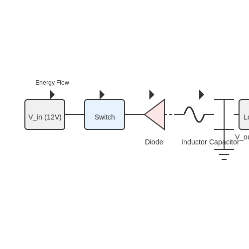
To understand how a buck converter operates, consider its fundamental components: a switching element (such as a MOSFET), an inductor, a diode, and output capacitors. The operation can be described in two primary phases within a switching cycle:
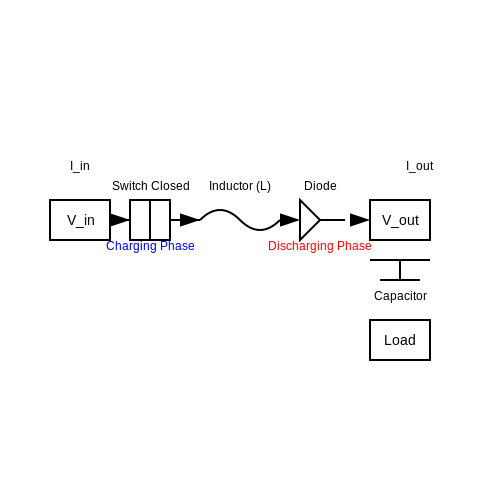
- On-Time: During this phase, the switch closes, supplying power to the inductor. The inductor stores energy by generating a magnetic field, while simultaneously increasing current flow through it.
- Off-Time: In this phase, the switch opens, and the energy stored in the inductor is transferred to the output load through the diode. The inductor discharges its energy, ensuring the output continues to receive power even when the switch is not conducting.
The average output voltage (\( V_{out} \)) can be derived using the relationship between the input voltage (\( V_{in} \)) and the duty cycle (\( D \)), given as:
where \( D \) is defined as the ratio of the time the switch is on to the total switching period. This relationship indicates that the output voltage is directly proportional to the input voltage and the duty cycle, providing a clear method to control voltage levels.
Practical Applications
The versatility of buck converters allows them to be utilized across various domains. Common applications include:
- Power Management Units: In portable electronic devices, buck converters optimize battery life by providing the required voltage to different components while minimizing energy losses.
- DC Motor Drives: These converters are often employed in motor control systems, where precise voltage control translates to improved performance and efficiency.
- Renewable Energy Systems: In solar power applications, buck converters allow for effective energy harvesting by matching the voltage levels of solar panels to battery storage systems.
In summary, the DC-DC buck converter is not just a fundamental element of power electronics but a vital technology in enhancing the efficiency and functionality of modern electronic devices. Its ability to adapt to varying electrical demands while efficiently managing power translates to higher performance and better utilization of resources in countless applications.
1.2 Advantages of Buck Converters
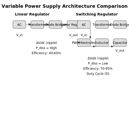
In the realm of power electronics, buck converters stand out due to their efficiency and versatility in regulating voltage levels. As we delve into the advantages of buck converters, it becomes clear how these systems optimize performance across various applications. At the forefront, one of the primary advantages of a buck converter is its high efficiency in converting direct current (DC) power from a higher voltage to a lower voltage. The efficiency typically exceeds 90%, significantly reducing energy losses compared to linear regulators, which dissipate excess voltage as heat. The efficiency of a buck converter can be quantitatively described using the equation: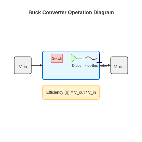
1.3 Applications of Buck Converters
DC-DC buck converters are widely utilized in both consumer and industrial applications due to their efficiency and ability to provide a stable output voltage from a higher input voltage. This component is essential in various contexts, where power density, heat reduction, and energy conservation are paramount. Below, we delve into several prominent applications of buck converters, highlighting their importance in modern technology.
Power Supply Circuits
One of the primary applications of buck converters is in power supply circuits. These converters step down DC voltage levels to accommodate components that require lower voltages to function correctly, exemplified by microcontrollers, FPGAs, and other digital circuits. As devices become increasingly efficient and integrated, the need for reliable power supplies has grown; hence, buck converters are critical in maintaining the operational integrity of these systems.
For instance, a microcontroller operating at 3.3V might be powered by a 12V battery. The buck converter steps down the voltage while maintaining high efficiency, often exceeding 90%, which signifies minimal power loss as heat.
Battery-Powered Devices
In battery-powered devices, such as smartphones, laptops, and other portable electronics, efficiency is paramount. Buck converters enable these devices to maximize battery longevity by providing high-efficiency power conversion. They can manage the power routing between the battery and various components flexibly, such as powering different parts of a circuit according to their instantaneous load requirements.
This adaptability is especially crucial in modern devices incorporating various functionalities, including Wi-Fi, Bluetooth, and high-resolution displays, which may have varying power requirements during different operational states.
Renewable Energy Systems
With the advent of renewable energy technologies, buck converters play a vital role in solar power systems and battery management systems. For example, when integrating solar panels with storage batteries, a buck converter can regulate the output voltage from the solar panel to charge the battery, ensuring that the battery receives appropriate voltage levels to maximize its lifespan and efficiency.
The application of buck converter strategies allows for better management of energy flow, preventing overcharging while optimizing the energy captured from solar panels.
Electric and Hybrid Vehicles
In the transportation sector, particularly with electric and hybrid vehicles, buck converters are instrumental in managing the power distribution between the battery pack and various vehicle systems such as the electric motor, HVAC (heating, ventilation, and air conditioning), and infotainment systems. These vehicles often use high-voltage battery systems, where a buck converter is necessary to supply lower voltages to auxiliary systems while maintaining efficiency across the board.
These converters not only help in optimizing performance but also extend the vehicle's operational range by conserving battery energy during excursions to various electrical demands.
Lighting Applications
Buck converters find applications in LED lighting systems, where they help adjust the power supplied to the LEDs to achieve the desired brightness levels while maintaining thermal efficiency. Since LEDs require precise voltage and current regulation, buck converters provide a stable output that adapts to fluctuations in input voltage due to changes in power sources or circuits.
This flexibility is advantageous in street lighting and automotive lighting applications, where reliable performance is critical.
Conclusion
Given the broad range of applications outlined, it is evident that buck converters are indispensable in modern electronic systems. Their ability to efficiently reduce voltage levels while minimizing losses ensures effective power management across various technologies, from portable devices to renewable energy systems and beyond. As the landscape of technology continues to evolve, the relevance and innovation surrounding buck converters are likely to expand, facilitating smarter, more efficient design choices in power electronics.
2. Basic Buck Converter Circuit
2.1 Basic Buck Converter Circuit
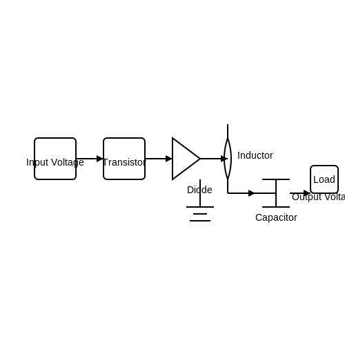
The buck converter is a vital component in modern electronics, serving as a key mechanism for voltage regulation. This power electronics device effectively steps down an input voltage to a lower output voltage, providing efficient power management in a compact size. Due to their efficiency, buck converters are extensively used in various applications ranging from battery-powered devices to industrial power systems.
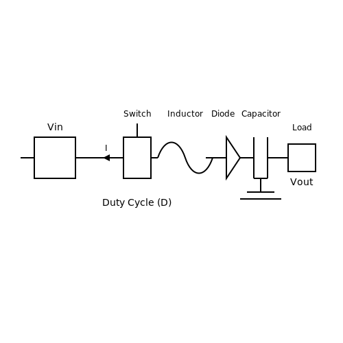
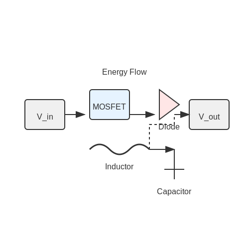
At its core, a basic buck converter consists of four principal components: a voltage source, a switch (usually a transistor), a diode, and an inductor, along with a capacitor as a load smoothing element. The operation relies on the switching action of the transistor to alternate between connecting and disconnecting the input voltage from the load. This process results in a pulsed output voltage that the inductor and capacitor subsequently smooth out into a more stable DC output.
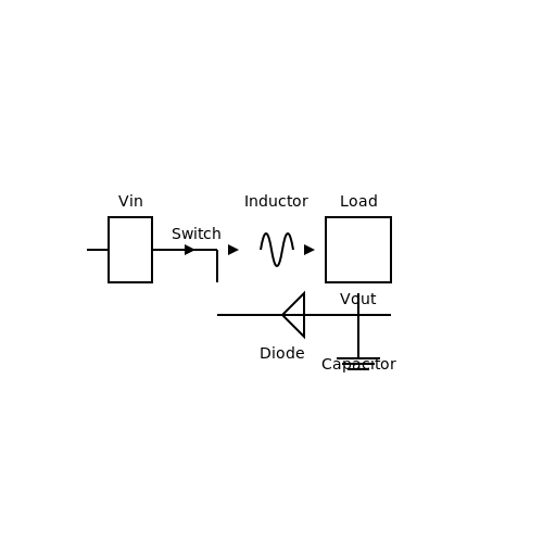
To understand the buck converter's function, consider a circuit arranged as follows: the input voltage source is connected to the switch, which is in series with the inductor. When the switch is closed, current flows through the inductor, leading to energy storage in the magnetic field. The inductor then releases this stored energy when the switch opens, allowing current to flow through the diode to the load. The inherent property of inductors to resist changes in current ensures that the current supplied to the load remains relatively steady.
This basic operational principle of the buck converter can be mathematically modeled. The output voltage ($${V_{out}}$$) of the buck converter is related to the input voltage ($${V_{in}}$$) and the duty cycle ($${D}$$) of the switch, which is defined as the fraction of one cycle in which the switch is closed. The relationship can be expressed as:
Where:
- $${D}$$ = Duty cycle (0 < $${D}$$ < 1)
- $${V_{in}}$$ = Input voltage
- $${V_{out}}$$ = Output voltage
For instance, if the input voltage is 12V and the duty cycle is set at 0.5 (or 50%), the output voltage would ideally be 6V. This individualized control allows buck converters to cater to diverse voltage requirements effectively.
In practical scenarios, the choice of components (e.g., inductor size, switch type) significantly influences converter efficiency and dynamic response. Furthermore, integrated circuit converters have been developed over the years, offering simplified designs and enhancing system reliability.
Understanding the design and operation of a basic buck converter is crucial for engineers working on power electronics systems. It lays the groundwork for exploring more complex converter designs, such as buck-boost or multi-phase converters, which can offer additional functionality or efficiency under varying load conditions.
The schematic diagram below illustrates a typical buck converter circuit, showcasing the arrangement of components and highlighting the flow of voltage and current during operation:
Through an exploration of the basic buck converter circuit, professionals can begin to appreciate its role in innovative electronic systems, enabling power efficiency and modular design. As we delve deeper into various applications, the principles laid out herein will serve as the foundation for further exploration into advanced configurations and enhancements.
2.2 Key Components and Their Functions
The operation of a DC-DC buck converter hinges upon several critical components, each playing a distinctive role in achieving efficient voltage step-down. To truly appreciate how these elements function synergistically, we will examine them individually, followed by an exploration of their interactions within the converter's topology.Inductor
The inductor is typically regarded as the heart of the buck converter. It stores energy during the "on" phase when the switch is closed and then releases it to the load during the "off" phase when the switch is open. The inductor's ability to smoothen the output current by mitigating rapid fluctuations is fundamental to the performance of the converter. To characterize the inductor, its inductance (L) can be defined by the relation:Switching Device
In the buck converter, the switching device—commonly a MOSFET—functions as an electronic switch that controls when the inductor is charged and discharged. When the MOSFET is turned on, current flows through the inductor, and when it is turned off, the current path is redirected through the diode to maintain output voltage. MOSFETs are preferred due to their high efficiency and rapid switching capabilities, crucial for applications where power loss must be minimized. The switching frequency (\( f_s \)) also crucially determines how effectively the converter maintains regulation and affects the size of passive components. A higher switching frequency can lead to smaller inductors and capacitors but may increase switching losses.Diode
The diode in a buck converter is responsible for providing a path for inductor current when the switching device turns off. Ideal diodes are fast-recovery diodes, designed to minimize reverse recovery time, thereby reducing associated losses. The operation of the diode can be modeled by the ideal diode equation:Capacitor
Capacitors in a buck converter serve dual roles: they filter the output voltage and store energy temporarily to smoothen load variations. High-frequency capacitors (like ceramic types) are often used at the output for filtering high-frequency noise, while electrolytic capacitors might be employed to provide bulk energy storage. The output voltage ripple can be estimated via:Control Circuit
While passive components handle the energy storage and release, the control circuit governs the switching actions. Typically utilizing a pulse-width modulation (PWM) technique, it adjusts the duty cycle of the switching device to regulate the output voltage effectively. An error amplifier compares the output voltage to a reference voltage, ensuring the system remains responsive to variations in load. The feedback loop balances stability and transient response by dictating how quickly the converter should react to changes, allowing modern buck converters to achieve remarkable efficiency, often exceeding 90%. Through understanding these components and their interactions, one can construct and optimize buck converters for various applications, from portable electronics to renewable energy systems. As we advance further into design considerations, the role of each of these components will become even more evident, especially when considering aspects such as thermal management and electromagnetic interference (EMI). Thus, mastering these elements is the key to successful power management in advanced electronic systems.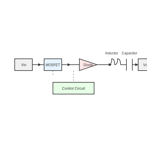
2.3 Switching Elements in Buck Converters
Understanding the Role of Switching Elements
In the architecture of a DC-DC buck converter, the switching elements play a critical role in voltage conversion and regulation. These elements are predominantly composed of transistors, which serve as electronic switches to control the output voltage by alternately connecting and disconnecting the input voltage from the output. The primary goal of utilizing switching elements is to allow for high efficiency in the conversion process. Traditional linear regulators dissipate excess voltage as heat, leading to inefficiencies especially when the input voltage significantly exceeds the desired output voltage. In contrast, buck converters typically achieve efficiencies ranging from 85% to over 95%, primarily due to the rapid switching characteristics of modern transistors.Types of Switching Elements
The choice of switching elements can significantly influence the performance of the buck converter. The two most common types of transistors used in these applications are MOSFETs (Metal-Oxide-Semiconductor Field-Effect Transistors) and BJTs (Bipolar Junction Transistors). Each type has its own set of advantages and disadvantages:- MOSFETs: They offer high input impedance, low output capacitance, and faster switching capabilities. This makes them highly favored in applications requiring rapid on-off switching, allowing for improved efficiency and reduced heat generation.
- BJTs: While they provide higher current capability, they generally have slower switching speeds and lower efficiency compared to MOSFETs. This can lead to increased heat dissipation and potentially lower overall performance in a buck converter application.
The Switching Mechanism
The operational dynamics of the switching elements can be understood through the buck converter’s phases: the ON state and the OFF state. In the ON state, the voltage from the input source is applied across the load, allowing current to flow. Conversely, when in the OFF state, the voltage is removed, and the inductor stores energy momentarily. During the transition between these states, the rapid switching introduces a phenomenon known as voltage ripple on the output. This ripple can be modeled as follows:Practical Considerations and Efficiency
Efficiency in buck converters directly correlates with the choice and design of the switching elements. For instance, the switching losses, which occur during the turning ON and OFF of the elements, add to the total power loss in the system. These losses can be quantified through the switching frequency and the characteristics of the transistors used, such as gate charge and capacitance. Choosing the appropriate switching frequency is a balancing act; higher frequencies can reduce the size of passive components but may also increase switching losses due to increased heat generation. As such, contemporary designs often utilize integrated circuits (ICs) that optimize switching characteristics while maintaining thermal management, contributing to improved overall converter efficiency.Real-World Applications
Buck converters with optimized switching elements have found considerable utility in diverse applications including consumer electronics, electric vehicles, telecommunications, and renewable energy systems. In electric vehicles, for instance, the efficiency of power converters can significantly impact the range and performance. Thus, engineers continuously innovate and research to develop higher efficiency converters using advanced semiconductor materials such as GaN (Gallium Nitride) and SiC (Silicon Carbide) transistors, which operate at higher voltages and temperatures while improving switching performance. In conclusion, the selection and application of switching elements in buck converters are pivotal not only to maximizing efficiency but also to enhancing the overall functionality and applicability of these vital components in modern electronic systems.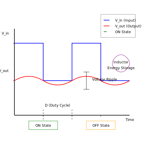
3. How Buck Converters Work
3.1 How Buck Converters Work
The operation of a buck converter, a type of DC-DC converter, is primarily based on the principles of inductive and capacitive energy storage, alongside switching techniques. Buck converters efficiently reduce a higher DC voltage to a lower DC voltage, and they are widely used in applications such as battery chargers, power supplies, and voltage regulators. Understanding how these converters function at a fundamental level will provide invaluable insights into their design and application.
Energy Storage in Buck Converters
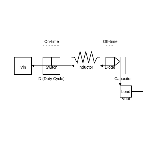
At the heart of a buck converter lies an inductor. Unlike resistive components, which dissipate energy as heat, inductors store energy in their magnetic field when current passes through them. The basic operation of buck converters can be understood through their working stages: On-time and Off-time, corresponding to the conduction and non-conduction states of the switching element, typically a transistor.
Working Principle
During the On-time, the switch (transistor) is closed. Current flows from the input supply through the switch and into the inductor, causing it to store energy. The corresponding voltage across the inductor can be described by Lenz's Law, which states that the induced electromotive force (EMF) opposes the change in current. Therefore, the voltage across the inductor \( V_L \) during this phase is:
Where \( L \) is the inductance and \( dI/dt \) is the rate of change of current. The energy stored in the inductor can then be expressed as:
During the Off-time, the switch opens, causing the inductor to release its stored energy. A diode, usually placed in parallel with the switch, allows the inductor current to flow to the output capacitor and load, maintaining the output voltage. The inductor continues to pass current to the load until its energy is fully discharged.
The output voltage \( V_{out} \) can be controlled by adjusting the duty cycle \( D \) of the switching signal. The relationship between the input voltage \( V_{in} \) and the output voltage for an ideal buck converter is given by:
Here, \( D \) is defined as the ratio of the On-time to the total switching period (On-time plus Off-time).
Real-World Applications
Buck converters find usage in a variety of applications due to their efficiency and reliability. In mobile gadgets, these converters are essential for managing battery life efficiently by providing the necessary voltage levels for different components, especially when multiple supply voltages must be generated from a single battery source. Furthermore, they are heavily used in renewable energy systems, powering low-voltage circuits from solar panels, and ensuring that electronic devices receive stable voltage levels despite fluctuations in input voltage.
Additionally, advancements in control techniques and semiconductor materials have further improved the performance of buck converters, allowing them to achieve higher efficiencies, reduced costs, and increased power density in modern applications. Understanding these fundamental principles lays the groundwork for engineers and researchers to innovate in this critical area of power electronics.
3.2 Voltage Conversion Ratio
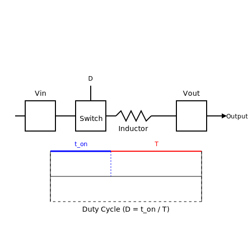
In the operation of a DC-DC buck converter, understanding the voltage conversion ratio is paramount to its design and application. The voltage conversion ratio defines the relationship between the input voltage and the output voltage, providing a clear depiction of the converter's efficiency in stepping down voltage. A well-designed converter maximizes this ratio while minimizing energy losses, optimizing performance for various applications. To derive the equation governing the voltage conversion ratio, we start with the basic principle of a buck converter, which utilizes a switch, typically a transistor, to regulate the voltage. When the switch is closed, input voltage is connected to the output and energy is stored in the inductor. When the switch opens, the inductor releases the stored energy to the load, resulting in a lower output voltage. The output voltage (\( V_{\text{out}} \)) can be mathematically expressed in relation to the input voltage (\( V_{\text{in}} \)) and the duty cycle (\( D \)). The duty cycle is defined as the fraction of time the switch is in the 'on' state during one switching period. It can be expressed as: $$ D = \frac{t_{on}}{T} $$ where \( t_{on} \) is the time the switch is closed, and \( T \) is the total switching period. Consequently, the relationship of the voltages is given by: $$ V_{\text{out}} = D \cdot V_{\text{in}} $$ Substituting the duty cycle expression into the equation we derived, we can express the output voltage as: $$ V_{\text{out}} = \left(\frac{t_{on}}{T}\right) \cdot V_{\text{in}} $$ This formula indicates that the output voltage is directly proportional to the input voltage scaled by the duty cycle. As a result, the voltage conversion ratio can be succinctly described: $$ \text{Voltage Conversion Ratio} = \frac{V_{\text{out}}}{V_{\text{in}}} = D $$ By manipulating the duty cycle, the converter can effectively achieve various output voltage levels. In practical applications, a typical range for the duty cycle in a buck converter might be from 0 to 1, which translates to the output voltage being adjustable from near zero to nearly equal to the input voltage. The conversion efficiency, however, can influence how close one can get to the maximum conversion range, with losses primarily arising from switching components and resistive paths. In real-world applications, the concept of voltage conversion ratio is significant across a spectrum of technology, including:- Power Supply Design: Engineers often use buck converters to create efficient power supplies for sensitive electronics, where precise voltage levels are essential.
- Renewable Energy Systems: In solar power systems, buck converters can optimize the voltage output from solar panels to batteries or grid connections.
- Electric Vehicles (EVs): Buck converters play a pivotal role in managing battery voltages throughout different operating conditions.
3.3 Efficiency Considerations
Efficiency is a critical performance metric for DC-DC buck converters, as it directly influences thermal performance, energy loss, and overall system cost. Understanding the factors affecting efficiency not only allows engineers to design more effective converters but also aids in the optimization of existing designs to achieve better performance characteristics.
One dominant aspect impacting efficiency is the voltage conversion ratio, which can be expressed mathematically through the relationship between the input voltage (Vin) and the output voltage (Vout). In ideal conditions, the efficiency (η) can be calculated as:
This equation indicates that, ideally, converters achieve maximum efficiency when the output voltage closely matches the input voltage. However, real-world applications often present a different scenario due to various losses involved in the conversion process, such as:
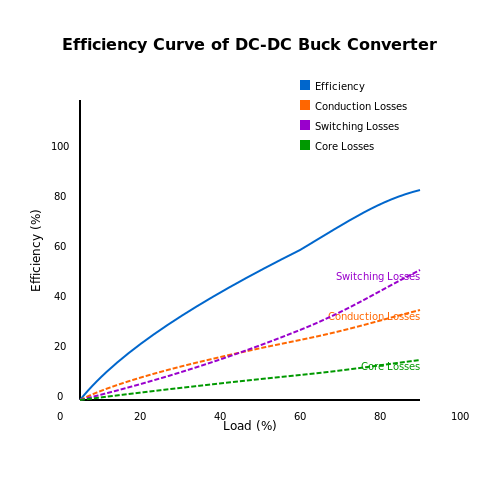
- Conduction Losses: These occur due to the on-resistance (Rds(on)) of the MOSFETs used in the switching stage. When the MOSFET is conducting, power loss can be described by:
where I is the output current. Understanding that higher output currents exacerbate conduction losses guides the selection of low Rds(on) devices for enhanced performance.
- Switching Losses: These losses occur during the transition periods when the MOSFETs switch on and off. The switching losses are contingent upon the switching frequency (fs), net capacitance at the switch nodes, and the duration of the transitions. A simplified expression for switching loss per cycle is:
where ton and toff are the turn-on and turn-off times, respectively. Accurate characterization of these timings is crucial to minimize losses and improve overall efficiency.
- Core Losses: In inductive components, core losses arise due to hysteresis and eddy currents, particularly at high frequencies. Optimization of the inductor, including selecting appropriate core materials and geometry, is essential in minimizing these losses.
As the switching frequency increases, although conduction losses may decrease due to lower average current over the switching period, the associated core and switching losses typically increase. Thus, a balance must be struck when selecting the switching frequency.
One critical real-world consideration is thermal management. Efficient designs must incorporate heat sinks or thermal pads to manage temperature rise due to these losses, ensuring reliable operation. Furthermore, optimizing PCB layout and component placement can greatly enhance thermal performance in practice.
The effectiveness of a buck converter can also be assessed through the efficiency curve, which typically peaks at specific loads. Examination of this curve can identify optimal operating conditions, aiding in practical applications where efficiency is paramount, such as in battery-powered devices where every joule counts.
In conclusion, when designing and optimizing a DC-DC buck converter, careful consideration of the losses discussed above is paramount. By employing low-loss components, optimizing switching frequency, and implementing robust thermal management strategies, engineers can achieve high efficiency while minimizing unnecessary energy waste.
4. Selecting Components
4.1 Selecting Components
When designing a DC-DC buck converter, the proper selection of components is critical for achieving the desired performance, efficiency, and reliability. Components such as the inductor, capacitor, switching device, and diode each play pivotal roles in the functioning of the converter. Understanding their specifications and operation principles allows engineers to tailor the converter to specific applications and load conditions.
Understanding Key Components
The fundamental components of a buck converter include:
- Inductor: Sizing and material properties directly influence the converter's efficiency and performance. The inductor smooths the output current and stores energy during operation.
- Capacitor: Capacitors are crucial for maintaining output voltage stability by filtering out voltage ripples. The equivalent series resistance (ESR) of the capacitor also impacts efficiency.
- Switching Device: Commonly, MOSFETs are selected due to their high efficiency and fast switching capabilities. The on-resistance and gate charge parameters significantly affect power losses.
- Diode: Schottky diodes are popular choices for converters due to their low forward voltage drop, which enhances efficiency. The reverse recovery time must also be considered to minimize switching losses.
Inductor Selection
Choosing the right inductor involves understanding the current requirements and the operating frequency. The inductance value (\(L\)) can be calculated using the formula:
Where:
- $$V_{in}$$: Input voltage
- $$V_{out}$$: Output voltage
- $$D$$: Duty cycle
- $$\Delta I_L$$: Allowed inductor current ripple
- $$f_{sw}$$: Switching frequency
The selection also depends on core material and saturation current ratings to ensure reliable performance under load transients.
Capacitor Considerations
The selection of the output capacitor is crucial for maintaining output voltage quality. The output voltage ripple (\(V_{ripple}\)) can be estimated by:
Where:
- $$I_{out}$$: Output load current
- $$C_{out}$$: Output capacitance
Selection should balance capacitance value, ESR, thermal performance, and physical size, especially in compact modern applications.
Switching Device and Diode Selection
MOSFETs are commonly used in buck converters due to their efficiency at high frequencies. Evaluating parameters such as threshold voltage, on-resistance, and gate charge is fundamental. To ensure the device can handle peak currents, consider the following equation:
Diodes must have a reverse voltage rating higher than the maximum input voltage and a forward current rating exceeding the output current. Preference should be given to Schottky diodes for their rapid recovery and low forward voltage drop.
Conclusion
Effective selection of components for a buck converter requires integrating theoretical knowledge with practical insights. Component choices not only affect immediate performance feedback but also long-term reliability and operational robustness. Different applications may demand various optimizations, thus tailored decisions based on specific use-cases will lead to superior designs.
4.2 Layout and Thermal Management
When designing a DC-DC buck converter, the layout and thermal management are critical factors that can significantly affect performance, efficiency, and reliability. A well-thought-out design helps in minimizing electrical noise, enhancing stability, and managing heat dissipation effectively. This section explores best practices for PCB layout and methods for thermal management in buck converters.
PCB Layout Considerations
In the physical implementation of a buck converter, the layout of the printed circuit board (PCB) plays a pivotal role in determining circuit performance. The goal is to minimize parasitic inductances and resistances while ensuring that the power can be transmitted efficiently from the input to the output without significant losses. Here are some critical considerations:
- Short and Wide Traces: Power traces should be as short and wide as possible to reduce resistive losses and voltage drop. Wider traces also help prevent overheating.
- Minimal Loop Area: The layout should minimize the loop area of the power circuit. This can be achieved by placing the input capacitor, switching components (like the MOSFETs), and output capacitor close together to reduce stray inductance and optimize performance.
- Grounding: A solid ground plane is essential. It provides a low-impedance return path for the currents and helps minimize EMI. Both the power and signal grounds should ideally be kept separate and then connected at a single point to avoid ground loop issues.
- Component Placement: Arrange components logically to ensure minimal interaction from inductive and capacitive elements. Sensitive components such as feedback circuits should be placed away from high-frequency components to avoid interference.
Ensuring a meticulous layout not only provides optimal performance but also aids in troubleshooting and reduces the potential for thermal issues.
Thermal Management Techniques
A buck converter's thermal performance can be a limiting factor in its overall design. High switching frequencies and the nature of the components involved can lead to considerable heat generation, necessitating effective thermal management strategies. Below are some methods commonly used:
- Heat Sinks: Attaching heat sinks to power components, particularly MOSFETs and inductors, can efficiently conduct heat away from the components into the surrounding air.
- Active Cooling: In scenarios with significant heat generation, such as high-power applications, utilizing fans or other active cooling methods can further decrease component temperatures.
- Thermal Pads: Using thermally conductive pads between components and heat sinks enhances thermal transfer by reducing thermal resistance.
- Temperature Monitoring: Incorporating temperature sensors and monitoring circuits into the buck converter design can enable better thermal management. By tracking temperature, the system can adjust the switching frequency or reduce the load as necessary to maintain safe operation conditions.
Understanding and implementing robust thermal management techniques will ensure the longevity and reliability of the buck converter while maximizing efficiency.
Real-World Applications
The principles of layout and thermal management are not merely theoretical; they hold significant implications in real-world applications. For instance:
- Consumer Electronics: Compact and efficient buck converters are crucial in devices like smartphones, tablets, and laptops, where thermal efficiency directly impacts performance and user experience.
- Electric Vehicles: High-power DC-DC converters in electric vehicles must manage heat efficiently under varying load conditions to ensure safety and reliability.
- Industrial Automation: In applications such as robotics and automation systems, efficient power management through advanced buck converters reduces energy costs and enhances system reliability.
In conclusion, a comprehensive approach to PCB layout and thermal management is essential in the design of DC-DC buck converters. By marrying theoretical principles with practical methodologies, engineers can create high-performance converters that meet the demands of modern applications.
4.3 Stability and Control Techniques
In the realm of DC-DC buck converters, the stability and control techniques play a fundamental role in ensuring optimal performance. As these converters are employed in various applications ranging from battery-powered devices to large-scale industrial power supplies, understanding how to maintain voltage regulation and prevent oscillations or instability is paramount. The stability of a buck converter primarily hinges on its feedback loop and control strategy. The feedback loop allows the converter to adjust its output based on various disturbances, such as changes in load or input voltage variations. Evaluating the stability of this system typically involves analyzing the phase margin and gain margin, two critical parameters that measure how far the system is from instability.Control Techniques
A variety of control techniques can be employed to enhance the stability of buck converters. The most common methods are voltage mode control and current mode control. Each of these strategies has its advantages and challenges, which we will explore to understand their effectiveness in maintaining stability. Voltage Mode Control regulates the output voltage by comparing it to a reference signal. The control loop adjusts the duty cycle of the switching signal to maintain the desired output voltage. While this method is relatively simple and requires fewer components, it tends to be less effective in response to rapid load changes. Specifically, voltage mode control may lead to suboptimal transient response or overshoot. In contrast, Current Mode Control incorporates an additional current loop that senses the inductor current in real time. By directly controlling the inductor current, this technique allows for better transient response and improved system stability. As a result, current mode control is often preferred in applications requiring swift load change responses. However, it also necessitates more complex circuitry, including an additional current sensing mechanism.Stability Analysis
When evaluating the stability of a buck converter, one useful approach is the Bode plot, which plots the gain and phase versus frequency. This analysis is invaluable in designing compensators to achieve desired stability properties. To construct a Bode plot, we start with the transfer function of the converter, which can typically be derived based on its circuit topology and control strategy. Assuming a simple buck converter with a small-signal model, the transfer function \( G(s) \) can be expressed in the following form:Real-World Applications and Emerging Trends
The selection of control techniques also reflects the needs of the application domain. For example, in automotive power supplies, where efficiency and response time are crucial, current mode control may be favored. Conversely, for less dynamic applications, voltage mode control could suffice due to its simplicity. Recent advancements in digital control techniques, including model predictive control (MPC) and adaptive control strategies, are also gaining traction. These methods offer further enhancements in maintaining stability under varying operational conditions and allow for reconfiguration of the control strategy based on real-time performance metrics. In summary, the stability and control techniques employed in DC-DC buck converters significantly influence their performance. By carefully selecting and tuning a control strategy, engineers can ensure that their designs meet the demands of modern applications, balancing efficiency, speed, and reliability.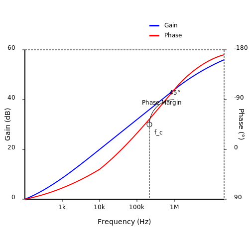
5. Voltage Mode Control
5.1 Voltage Mode Control
Voltage mode control is a widely utilized technique in the operation of DC-DC buck converters. Unlike current mode control, which regulates output current, voltage mode control focuses on achieving stable output voltage levels, making it especially beneficial in applications where maintaining constant voltage is paramount.
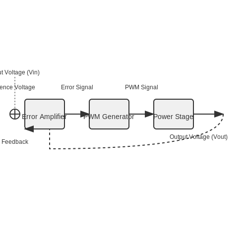
In essence, voltage mode control involves comparing the output voltage to a reference voltage and generating an error signal that directs the converter's behavior. This error signal feeds into a pulse width modulation (PWM) modulator, which adjusts the duty cycle of the switching element in the buck converter. The PWM signal controls the duration for which the switch is closed, directly impacting the output voltage.
Theoretical Foundation
To deeply understand voltage mode control, we can develop the fundamental equation governing this control strategy. The basic operating principle of a buck converter can be expressed in terms of its duty cycle, denoted as \(D\). For an ideal buck converter with a fixed input voltage \(V_{in}\) and resistive load \(R\), the output voltage \(V_{out}\) relates to the input voltage and duty cycle as follows:
This relationship indicates that as the duty cycle is adjusted, the output voltage can be finely tuned. However, a direct relationship to variations in output load and input voltage necessitates careful control strategies to prevent undesirable fluctuations.
Control Loop Dynamics
The control loop in a voltage mode converter typically consists of three main components: the error amplifier, the PWM generator, and the power stage. The error amplifier receives feedback from the output voltage and compares it to a reference voltage, generating an error signal that represents the difference. The subsequent PWM generator takes this error signal and modulates the width of the output pulse accordingly.
An essential element in voltage mode control is the compensator. The compensator is designed to adjust the gain and phase response of the control loop, thereby enhancing system stability and transient response. Commonly used compensators include lead, lag, and PID compensators, each offering unique benefits in dynamic response and steady-state accuracy.
System Stability
The stability of a voltage mode controlled system can be analyzed using techniques such as Bode plots and root locus methods. The design must account for the effects of parasitic elements in the circuit, which can influence the dynamic performance. Analyzing the loop gain, which is the product of the gain of the compensator and the power stage, is crucial in determining system stability margins.
In practice, engineers often employ simulation tools like SPICE to model the buck converter's behavior under various loading conditions, allowing them to tweak the control parameters before implementation. This simulation phase is critical, as it can reveal potential issues such as suboptimal transient response or instability due to phase margin reduction.
Real-World Applications
Voltage mode control is prevalent in numerous applications, particularly in portable electronic devices where battery management is crucial. It is also utilized in power supplies for computer systems and telecommunications equipment, where even minor variations in voltage can lead to performance degradation or failure. In solar inverters and renewable energy systems, accurate voltage regulation is vital for safe integration with the power grid.
In conclusion, voltage mode control is a foundational concept in the operation of DC-DC buck converters. Understanding its principles allows engineers to design robust and efficient power supply systems capable of meeting the demanding voltage stability requirements of modern electronics.
5.2 Current Mode Control
The efficacy of a DC-DC buck converter lies not only in its architecture but also in the control strategies employed to regulate and optimize its performance. Among these, current mode control stands out for its robust performance, efficiency, and ability to simplify circuit design. This subsection delves into the intricacies and applications of current mode control in the context of buck converters.
Current mode control techniques focus on regulating the output voltage of a buck converter while simultaneously controlling the inductor current. Unlike voltage mode control, where feedback is based solely on the output voltage, current mode control introduces an additional layer of feedback, allowing for improved transient response and inherent protection against overcurrent conditions.
Fundamental Concepts of Current Mode Control
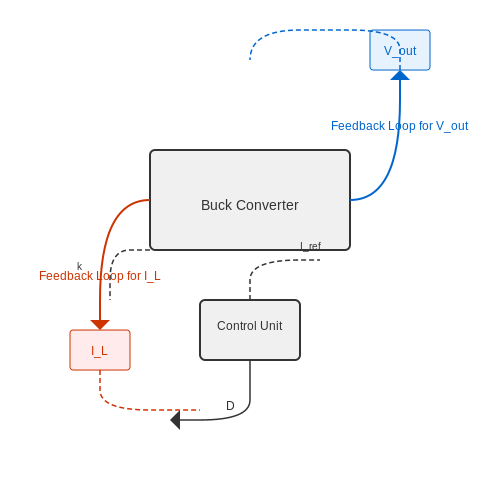
At its core, current mode control utilizes two primary feedback loops: the output voltage loop, similar to traditional control methods, and an inner current loop that monitors and regulates the inductor current. This dual-loop architecture facilitates faster response to load transients and provides greater stability in comparison to voltage mode control.
One of the fundamental benefits is the integration of peak current limiting, which protects the power stage from excessive stress. This feature becomes crucial in applications where sudden load changes could lead to inductor saturation or component failure.
Mathematical Formulation
To illustrate current mode control, let’s derive the control law that governs the relationship between the output voltage (Vout) and the inductor current (IL). The output voltage can be indirectly controlled by adjusting the duty cycle (D) of the converter. The relationship can be expressed as:
Where Vin is the input voltage. Introducing current mode, we can state that the inductor current is controlled not just by duty cycle, but through a current reference signal (Iref) derived from a proportional feedback of the output voltage:
Here, k is a proportional gain factor. The duty cycle is adjusted based on the comparison between the sensed inductor current and the reference current:
These equations define a relationship whereby the duty cycle dynamically responds to variations in load current, creating a more adaptive control system compared to traditional methods.
Practical Implications and Applications
The application of current mode control in buck converters can be found in various domains including power supplies, renewable energy systems, and mobile devices. In power supplies, the rapid response to changing loads minimizes output voltage overshoot and undershoot, enhancing overall system stability.
In renewable energy applications, such as solar inverters, current mode control enables effective management of energy harvesting and load matching, ensuring optimal power transfer despite fluctuating input conditions. Furthermore, in mobile devices, maintaining efficiency while managing thermal constraints is critical, making current mode control an attractive choice.
In summary, current mode control offers significant advantages, particularly in systems requiring fast dynamic response and built-in safety measures. As demands for efficiency and reliability increase in electronics design, the relevance of this control technique continues to grow.
5.3 Hysteretic Control
The efficiency and responsiveness of DC-DC buck converters are crucial for a multitude of applications ranging from battery-powered devices to industrial power supplies. One advanced technique used to enhance these properties is hysteretic control. This control methodology offers both simplicity and performance improvements, especially under varying load conditions.
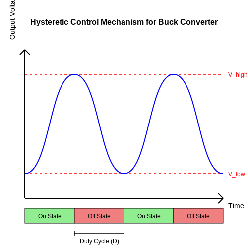
At its core, hysteretic control utilizes a feedback mechanism based on output voltage and inductor current. By monitoring these parameters, the converter can dynamically adjust its operating state to maintain the desired output voltage. Unlike traditional voltage mode control, where the feedback loop operates continuously, hysteretic control activates the switching elements based on pre-defined voltage thresholds, leading to quick transient responses.
Principles of Hysteretic Control
The fundamental operational principle of hysteretic control is rooted in the concept of hysteresis, which is defined as the dependence of a system's output on its past inputs. In the context of a buck converter, hysteresis allows for a controlled range of output voltage deviation before adjustments are made. The key parameters are:
- Upper Voltage Threshold (Vhigh): The output voltage at which the switch turns off to prevent output over-voltage.
- Lower Voltage Threshold (Vlow): The output voltage at which the switch turns on to restore the output voltage to the desired level.
This creates a band around the desired output voltage, and rapid switching between on and off states occurs, based on whether the output voltage is above or below these threshold levels. The result is a control philosophy that prioritizes stability and quick response, making it advantageous in applications with rapidly changing load conditions.
Mathematical Modeling of Hysteretic Control
To better understand hysteretic control within a buck converter, let’s derive the equations governing the switching behavior. Given an ideal buck converter with input voltage \( V_{in} \), output voltage \( V_{out} \), and an effective duty cycle \( D \), the output voltage can be modeled as:
In hysteretic control, duty cycle adjustments are crafted based on how far the output voltage strays from the defined voltage thresholds:
When \( V_{out} \) exceeds \( V_{high} \), the converter switches off:
When \( V_{out} \) drops below \( V_{low} \), the converter switches on again:
This toggling of the duty cycle enables significant adaptability for load variations. The key advantage is that hysteretic control minimizes the loop complexity and accomplishes fast dynamic response times, making it ideal for applications in digital systems and other environments requiring efficiency and stability.
Real-World Applications
The practical implications of hysteretic control are numerous. Many consumer electronics, such as laptops and smartphones, leverage this control technique in their power management systems to prolong battery life while ensuring performance. Similarly, industrial automation systems benefit from hysteretic control through improved efficiency and reduced electromagnetic interference.
More advanced implementations, such as those used in electric vehicles and renewable energy systems, capitalize on the rapid response times enabled by hysteretic control to manage varying input supplies and loads effectively, contributing to overall system robustness.
In summary, hysteretic control offers a dynamic, efficient, and responsive approach to managing power conversion in DC-DC buck converters, thereby playing a crucial role in modern electronic systems.
6. Power Management in Consumer Electronics
6.1 Power Management in Consumer Electronics
In the rapidly advancing field of consumer electronics, efficient power management is a crucial factor influencing device performance and longevity. One of the most efficient solutions to regulate voltage levels and ensure optimal power utilization is the implementation of DC-DC buck converters. Understanding their role and application in power management provides critical insights for engineers and researchers alike.
At its core, a buck converter is a type of switched-mode power supply (SMPS) that transforms a higher input voltage into a lower output voltage, allowing for greater efficiency when powering devices. Compared to linear regulators, which waste excess energy as heat, buck converters operate with much higher efficiency, often exceeding 90%. This efficiency becomes paramount in modern devices, where compactness and battery longevity are essential.
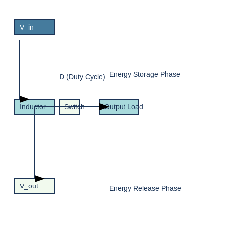
The operational principle of a buck converter revolves around storing energy in an inductor during the "on" phase and releasing it to the load during the "off" phase of the switching cycle. More specifically, when the switch is closed, current flows through the inductor, building up magnetic energy. When the switch opens, the inductor releases this energy to the output, providing a reduced voltage supply to the load. This process can be described mathematically as follows:
Here, \( V_{out} \) is the output voltage, \( D \) is the duty cycle defined as the ratio of the time the switch is closed to the total time of the cycle, and \( V_{in} \) is the input voltage. By controlling the duty cycle \( D \), the output voltage can be effectively regulated to meet the specific power requirements of the load. This regulation is critical in devices such as smartphones, laptops, and other portable electronics where battery life and efficient power draw are vital.
Applications in Consumer Electronics
DC-DC buck converters are ubiquitous in consumer electronics. They are integrated into various devices to ensure efficient power management while enabling reduced form factors. For instance, in mobile phones, buck converters supply power to the main CPU and other components from the lithium-ion battery, effectively maintaining energy efficiency across different operational states. Similarly, in laptops and tablets, buck converters manage power to both high-performance and auxiliary components, optimizing battery usage.
Moreover, the flexibility in design and the ability to scale down output voltages support the increasing demand for smaller and more powerful electronics. In circuits where multiple voltage levels are needed, buck converters are often paired with other DC-DC converter types—such as boost converters—to create complete power management solutions. This synergy not only enhances the overall performance of electronic systems but also contributes to their reliability and safety.
Trends and Future Directions
As consumer electronics continue to evolve, the demand for energy-efficient solutions like buck converters is expected to rise. The integration of advanced control techniques, such as adaptive and digital control methods, is paving the way for even higher efficiency and more precise output voltage regulation. Furthermore, ongoing research into wide-bandgap semiconductors promises to enhance the performance characteristics of b uck converters, enabling them to operate at higher frequencies with lower losses, ultimately catering to the needs of future electronic applications.
In summary, understanding the intricacies of buck converters is essential for anyone involved in the design and development of advanced consumer electronics. Their ability to efficiently manage power while accommodating the demands of modern devices makes them invaluable in today's fast-paced technological landscape.
6.2 Electric Vehicles and Renewable Energy Integration
In recent years, the integration of renewable energy sources and electric vehicles (EVs) has gained immense traction, driven by the need for sustainability and the reduction of greenhouse gas emissions. The DC-DC buck converter plays a pivotal role in this integration by enabling efficient voltage regulation required in various applications. The following discussion elaborates on the significance of buck converters in the realms of electric vehicles and renewable energy.
Understanding the Role of Buck Converters
Buck converters are essential in managing power flow and efficiency. Their ability to step down voltage while maintaining power provides an ideal solution for extracting maximum energy from renewable sources, such as solar panels and wind turbines. Additionally, they assist in regulating the voltage supplied to electric vehicle batteries, ensuring that they operate within optimal ranges throughout their charge and discharge cycles.
Electric Vehicle Applications
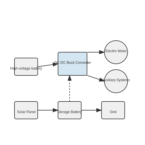
In electric vehicles, the use of a DC-DC buck converter facilitates the effective management of power distribution among various components, including the motor, auxiliary systems, and onboard charging units. By converting high-voltage battery power to the lower voltage levels needed for these subsystems, the buck converter enhances system efficiency and extends the driving range of EVs.
Expanding beyond merely supplying power, modern buck converters are equipped with advanced control mechanisms that enable regenerative braking systems. During braking, kinetic energy from the vehicle is converted back into electrical energy and stored in the battery, with the buck converter optimizing the voltage output to ensure safe charging without damaging the battery.
Integration with Renewable Energy Systems
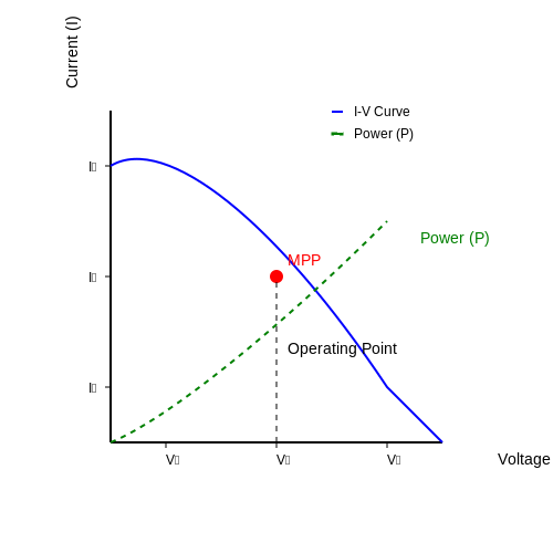
When coupled with renewable energy sources, buck converters facilitate the integration of variable energy outputs into the electrical grid. For instance, in solar energy systems, a buck converter can effectively match the output voltage of solar panels to the required voltage of storage batteries or grid systems. This role is crucial for maximizing energy capture from natural sources despite fluctuating environmental conditions.
Moreover, smart grid technology increasingly relies on buck converters to harmonize supply and demand in real-time, thereby enhancing grid stability. By mitigating voltage spikes and maintaining a steady output, buck converters contribute significantly to the resilience of the power systems, particularly in regions prone to voltage instability.
Future Trends and Innovations
As EV technology continues to evolve, so too does the design and functionality of buck converters. Innovations such as integrated circuit designs and advanced control algorithms are expected to further enhance their efficiency and reduce their footprint. This optimization is vital to meet the strict energy efficiency standards set forth in many regions as a commitment to reducing carbon emissions.
Furthermore, exploring wide-bandgap semiconductor materials, such as silicon carbide (SiC) and gallium nitride (GaN), may lead to significant advancements in buck converter efficiency and heat dissipation, fostering their implementation in high-power applications like electric buses and heavy machinery.
In conclusion, as the demand for electric vehicles and renewable energy solutions continues to rise, the role of DC-DC buck converters becomes increasingly critical. Their capability to efficiently manage power conversion remains at the forefront of both electric vehicle technology and renewable energy integration, marking them as indispensable components of future sustainable energy systems.
6.3 Emerging Technologies and Innovations
As the demand for more efficient and compact power management solutions continues to rise, the field of DC-DC buck converters is witnessing significant innovations and advancements. This section explores some of the most promising emerging technologies that are likely to reshape the landscape of buck conversion, alongside their real-world applications and benefits.Advanced Materials and Components
The effectiveness of buck converters is heavily influenced by the quality of materials used in their construction. Recent innovations in semiconductor materials have the potential to enhance performance drastically. For instance, wide-bandgap semiconductors such as silicon carbide (SiC) and gallium nitride (GaN) offer lower on-resistance, higher thermal conductivity, and improved efficiency compared to traditional silicon-based components. These characteristics allow for operation at higher frequencies, which can reduce the size of passive components like inductors and capacitors. The impact of these materials is most notable in applications such as electric vehicles (EVs) and renewable energy systems, where efficiency and weight savings are critical. For example, GaN converters can achieve efficiencies exceeding 98%, significantly enhancing battery range and performance in EVs.Integration of Digital Control Techniques
The integration of digital control methods is revolutionizing the design and performance of buck converters. Digital controllers enable more precise regulation of output voltage and current, with the ability to implement sophisticated algorithms such as model predictive control (MPC) and adaptive control strategies. This adaptability not only enhances efficiency but also minimizes the response time to load transients, which is vital for modern electronics demanding stable power supplies. Furthermore, digital control systems facilitate real-time monitoring and diagnostics, allowing designers to implement preventive maintenance strategies. This capability is particularly beneficial in industrial applications, where equipment reliability is paramount.Modeling and Simulation Enhancements
The advent of advanced simulation tools has transformed the design process for buck converters. Enhanced modeling techniques, including dynamic switching models and thermal simulations, allow engineers to predict performance under various operating conditions effectively. Coupled with the use of artificial intelligence (AI) and machine learning (ML), these tools can optimize circuit designs more rapidly and accurately than traditional methods. For instance, machine learning algorithms can analyze historical performance data and suggest improvements in design parameters, leading to reductions in development time and costs. These innovations open doors for rapid prototyping and testing in high-tech industries, ensuring faster market readiness of electronic devices.Miniaturization through Integrated Solutions
The trend toward miniaturization in electronics has led to the development of integrated power modules that combine multiple components within a single package. These integrated solutions can significantly reduce the footprint of the DC-DC converter while greatly simplifying the circuitry. Innovations in packaging technologies, such as multi-chip module (MCM) technology, further push the boundaries of size and efficiency. These advancements are particularly critical in portable electronics, where space is at a premium. By incorporating transformers, inductors, and capacitors into a single module, manufacturers can deliver compact devices without sacrificing performance.Future Prospects and Conclusions
As we look to the future, the ongoing research into intelligent materials, digital controls, and integration techniques promises to create even more efficient and compact DC-DC buck converters. Innovations such as wireless power transfer and hybrid energy systems may soon leverage these advancements to further influence how power management is approached in various industries. In summary, understanding these emerging technologies is vital for engineers and researchers aiming to develop cutting-edge solutions that address the ever-evolving demands of modern power electronics. These innovations not only enhance performance but are also paving the way for more sustainable and efficient systems across diverse applications.7. Books and Textbooks
7.1 Books and Textbooks
- Power Electronics Handbook — This comprehensive guide covers devices, circuits, and applications in power electronics. It is particularly well suited for engineers looking to delve deep into the principles and applications of power converters, including DC-DC buck converters.
- Modern Control Engineering — This textbook incorporates control engineering concepts applicable to power electronics, providing a theoretical backbone that's essential for advanced study, especially for those looking into control strategies for converters.
- Pulse-width Modulated DC-DC Power Converters — An excellent resource focusing on the pulse-width modulation (PWM) strategies used in DC-DC converters, discussing various modulations and their implementation in buck converters in detail.
- Power Electronics: Principles and Applications — This textbook provides insights into the foundational principles of power electronics, with ample focus on DC-DC buck converters, and is essential for understanding various applications and practical implementations.
- Fundamentals of Power Electronics — An authoritative academic resource that meticulously addresses the mathematical formulations involved in power electronics, providing step-by-step derivations of key equations related to buck converters.
- Power Electronics and Motor Drives — Useful for those interested in how power electronics interface with motor drive applications, including a section dedicated to DC-DC buck converters used in these systems.
- Low-Power and High-Sensitivity Integrated Circuits and Systems — Focused on the design of low-power circuits, this book covers key insights into designing efficient DC-DC buck converters, an essential read for minimizing power loss in electronic systems.
7.2 Research Papers and Articles
- Design and Analysis of Buck Converter for PV Systems — This IEEE paper discusses the design considerations for buck converters within photovoltaic systems, focusing on efficiency and performance optimization.
- Comparison of Different Topologies of DC-DC Converter — The paper provides a comprehensive comparison and analysis of various DC–DC converter topologies, examining their suitability across different applications.
- Digital Control for Interleaved Buck Converter Used in Distributed Power Supply Systems — Explores innovative control strategies for interleaved buck converters, improving performance, and reliability in distributed energy systems.
- Design and Implementation of a Digital Peak Current Mode Control of a High-Frequency Buck Converter — SAGE Publications offer insights into digital control methodologies for high-frequency buck converters to enhance system response and efficiency.
- High-Efficiency Buck-Boost DC–DC Converter for Photovoltaic Energy System — A detailed study on a buck-boost converter configuration aimed at maximizing the efficiency in photovoltaic applications published in ScienceDirect.
- A Modified Hysteresis Current Control Scheme for a Synchronous Buck Converter — This paper presents advancements in hysteresis current control techniques to improve dynamic performance in synchronous buck converters.
- Buck Converter Design and Optimization for Electronics Applications — A case study that discusses the design challenges and optimization strategies for buck converters in various electronic applications.
7.3 Online Resources and Courses
For those delving deeper into the world of DC-DC buck converters, online resources and specialized courses can offer the advanced knowledge and nuanced insights required for mastering this important component of power electronics. Below is a carefully curated list of high-quality online resources, including advanced courses, scholarly articles, and comprehensive tutorials, designed to expand your understanding and technical prowess in this area.
- Power Electronics Specialization by University of Colorado — This Coursera course, part of a specialization, offers in-depth lectures on power electronics, including DC-DC converters, with practical design projects.
- MITx: 6.007 Electronics and Circuits — Free online course hosted by edX, offering expert lectures on electrical circuits, with a comprehensive module on DC-DC converters.
- Texas Instruments Learning Platform — Provides detailed tutorials focusing on practical applications of DC-DC buck converters, suitable for those with engineering backgrounds.
- All About Circuits - DC-DC Converters — A comprehensive electronics textbook chapter online, focusing on the principles and design of buck converters.
- MIT OpenCourseWare: Dynamic Systems and Control — Offers numerous free lecture notes and resources for advanced dynamics and control systems, useful in optimizing DC-DC converter performance.
- YouTube - Power Electronic Converters and Systems by Dr. Bhim Singh — A YouTube playlist providing deep theoretical insights into various DC-DC converter topologies, including buck converters, from a renowned expert.
- Instructables - Understanding and Characterizing Switch Mode DC-DC Converters — Offers hands-on guide and practical projects to explore the functionalities and performance of buck converters through experimentation.
- International Rectifier University Program — Provides an array of educational materials useful for understanding the intricacies of buck converters and power conversion.