RF Signal Generation Techniques
1. Basic Principles of RF Signals
Basic Principles of RF Signals
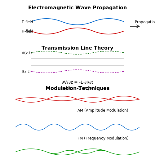
Radio frequency (RF) signals are electromagnetic waves characterized by frequencies ranging from 3 kHz to 300 GHz, occupying a critical portion of the electromagnetic spectrum. These signals are governed by Maxwell's equations, which describe the propagation of electromagnetic fields through space. The fundamental relationship between electric (E) and magnetic (H) fields in free space is given by:
where μ is the permeability, ϵ is the permittivity, and J represents the current density. In lossless media, these equations simplify to wave equations that describe propagating plane waves:
Wave Propagation and Transmission Line Theory
At RF frequencies, signal wavelengths become comparable to the physical dimensions of conductors, necessitating transmission line theory for accurate analysis. The telegrapher's equations describe voltage (V) and current (I) propagation along a transmission line:
where R, L, G, and C represent the per-unit-length resistance, inductance, conductance, and capacitance, respectively. For lossless lines (R = G = 0), these equations yield a propagation constant (γ) and characteristic impedance (Z₀):
Modulation Techniques
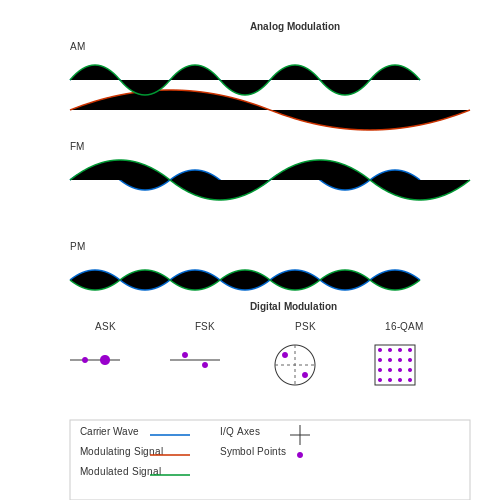
RF signals are typically modulated to encode information. The three fundamental analog modulation schemes are:
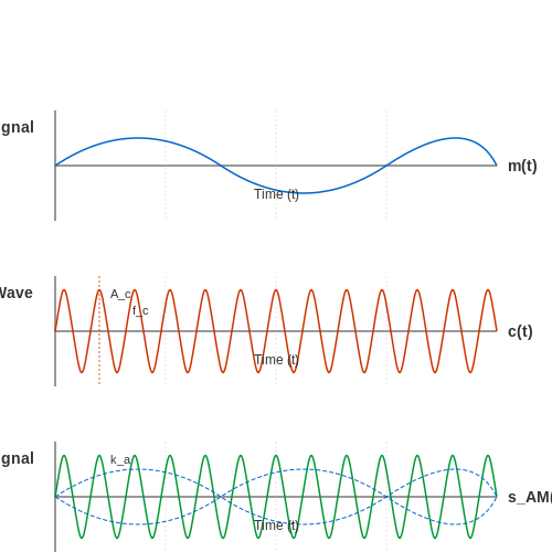
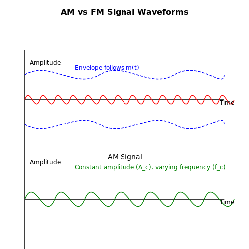
- Amplitude Modulation (AM): The carrier amplitude varies with the message signal.
- Frequency Modulation (FM): The carrier frequency varies with the message signal.
- Phase Modulation (PM): The carrier phase varies with the message signal.
For digital communication, common schemes include:
- Amplitude Shift Keying (ASK)
- Frequency Shift Keying (FSK)
- Phase Shift Keying (PSK)
- Quadrature Amplitude Modulation (QAM)
The mathematical representation of a modulated carrier is:
where A(t) is the time-varying amplitude and ϕ(t) is the time-varying phase.
Signal-to-Noise Ratio and Link Budget
The performance of RF systems is fundamentally limited by noise. The signal-to-noise ratio (SNR) is a critical metric:
where Psignal is the signal power and Pnoise is the noise power. The noise power is given by:
where kB is Boltzmann's constant, T is the system temperature, and B is the bandwidth.
Link budget analysis accounts for all gains and losses in an RF system:
where Prx is the received power, Ptx is the transmitted power, Gtx and Grx are antenna gains, and Lpath is the path loss.
Impedance Matching and Reflection Coefficient
Maximizing power transfer requires impedance matching between components. The reflection coefficient (Γ) quantifies impedance mismatch:
where ZL is the load impedance and Z0 is the characteristic impedance. The voltage standing wave ratio (VSWR) relates to Γ by:
1.2 Frequency and Wavelength Considerations
Fundamental Relationship Between Frequency and Wavelength
In RF signal generation, the frequency (f) and wavelength (λ) of an electromagnetic wave are intrinsically linked by the speed of propagation, which in free space is the speed of light (c ≈ 3 × 10⁸ m/s). The relationship is given by:
For example, a 1 GHz signal has a wavelength of approximately 30 cm in free space. This inverse proportionality means higher frequencies correspond to shorter wavelengths, influencing antenna design, transmission line behavior, and signal propagation characteristics.
Propagation Medium Effects
The speed of propagation (v) decreases in dielectric media due to the relative permittivity (εr) and permeability (μr). The wavelength in a medium becomes:
In coaxial cables with PTFE insulation (εr ≈ 2.1), a 2.4 GHz Wi-Fi signal's wavelength reduces from 12.5 cm (free space) to 8.6 cm. This wavelength compression must be accounted for in distributed-element circuit design, such as quarter-wave transformers.
Phase Velocity and Group Delay
The phase velocity (vp) describes how quickly the wave's phase propagates, while group velocity (vg) determines energy transfer speed. For TEM modes:
In dispersive media where vp ≠ vg, pulse distortion occurs—a critical consideration for ultra-wideband (UWB) systems. Microstrip lines exhibit frequency-dependent effective permittivity, requiring full-wave simulation for accurate phase matching in array antennas.
Skin Depth and Conductor Losses
At RF frequencies, current crowds near conductor surfaces due to the skin effect. The skin depth (δ) determines the effective conduction thickness:
For copper (σ = 5.8 × 10⁷ S/m) at 10 GHz, δ ≈ 0.66 μm. This mandates surface roughness optimization in PCB traces and waveguide coatings to minimize resistive losses, particularly in millimeter-wave applications.
Fractional Bandwidth Constraints
Many RF components exhibit performance tied to fractional bandwidth (FBW), defined as:
A quarter-wave resonator at 5 GHz with 10% FBW maintains consistent impedance from 4.75–5.25 GHz. Beyond this range, higher-order modes degrade performance—a limitation overcome in multi-section matching networks or tunable filters using varactors.
Practical Design Implications
- Antenna Arrays: Element spacing must be ≤ λ/2 to avoid grating lobes in phased arrays.
- Filter Design: Coupled-line filters require λ/4 resonators with precisely controlled even/odd mode impedances.
- Radar Systems: Range resolution ΔR = c/(2B) demands ultra-wideband chirps (e.g., 77 GHz automotive radar with 4 GHz bandwidth achieves ~3.75 cm resolution).
Modulation Techniques Overview
Fundamental Modulation Classes
RF signal modulation techniques are broadly classified into analog and digital domains. Analog modulation varies a continuous waveform's parameters, while digital modulation encodes discrete symbols. The three fundamental analog techniques are:
- Amplitude Modulation (AM): Varies carrier amplitude proportionally to the message signal
- Frequency Modulation (FM): Alters carrier frequency based on the modulating signal
- Phase Modulation (PM): Shifts carrier phase in accordance with input signal
These techniques form the basis for more complex digital modulation schemes. The general expression for a modulated carrier wave is:
Digital Modulation Fundamentals
Digital modulation maps discrete symbols to specific waveform states. The key parameters are:
- Symbol Rate (Baud Rate): Number of symbol changes per second
- Bit Rate: Actual information rate in bits per second (bps)
- Constellation Diagram: Visual representation of symbol states in I/Q plane
The relationship between bit rate (Rb) and symbol rate (Rs) is:
where M is the number of possible symbols.
Key Digital Modulation Types
Amplitude-Shift Keying (ASK)
Varies carrier amplitude among discrete levels. Binary ASK (BASK) uses:
Frequency-Shift Keying (FSK)
Switches between predefined frequencies. The modulated signal is:
Phase-Shift Keying (PSK)
Changes carrier phase in discrete steps. For M-ary PSK:
Advanced Modulation Schemes
Modern systems employ sophisticated techniques combining amplitude and phase modulation:
- Quadrature Amplitude Modulation (QAM): Simultaneously varies amplitude and phase
- Orthogonal Frequency Division Multiplexing (OFDM): Uses multiple orthogonal subcarriers
- Spread Spectrum Techniques: Includes DSSS and FHSS for interference mitigation
The spectral efficiency η of a modulation scheme is given by:
where B is the bandwidth occupied by the modulated signal.
Modulation Trade-offs in Practical Systems
Selection criteria for modulation techniques involve balancing:
- Power Efficiency: Required Eb/N0 for target BER
- Bandwidth Efficiency: Data rate per unit bandwidth
- Implementation Complexity: Transceiver hardware requirements
- Robustness: Performance under channel impairments
The Shannon-Hartley theorem establishes the fundamental limit:
where C is channel capacity, B is bandwidth, and S/N is signal-to-noise ratio.
2. Oscillator Circuits: LC and Crystal Oscillators
Oscillator Circuits: LC and Crystal Oscillators
LC Oscillators
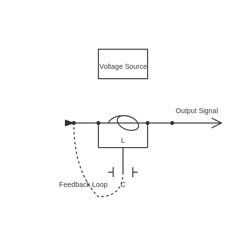
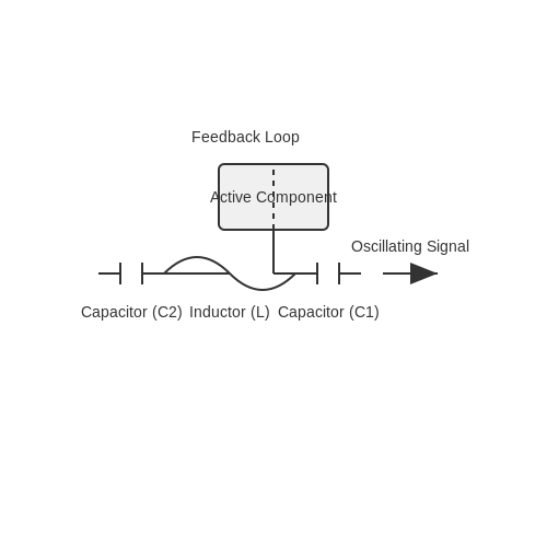
LC oscillators rely on the resonant properties of an inductor-capacitor (LC) tank circuit to generate periodic signals. The resonant frequency f0 of an ideal LC circuit is given by:
where L is the inductance and C is the capacitance. In practice, losses in the components and parasitic elements modify this relationship. The quality factor Q of the tank circuit determines the oscillator's phase noise performance and frequency stability:
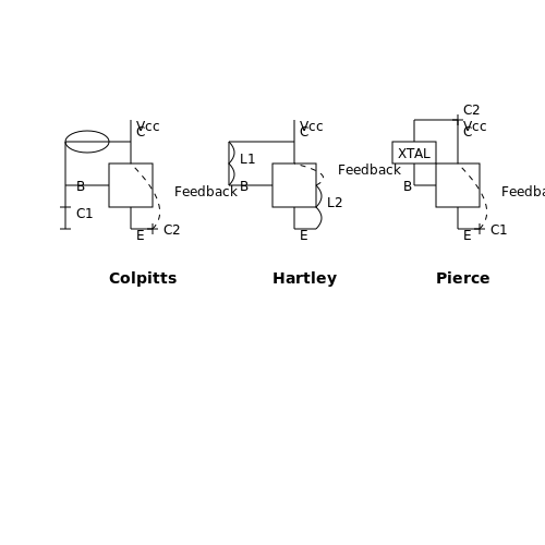
Common LC oscillator topologies include:
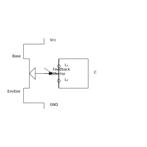
- Colpitts oscillator - Uses a capacitive voltage divider for feedback
- Hartley oscillator - Employs inductive feedback through a tapped coil
- Clapp oscillator - Variant of Colpitts with an additional series capacitor
In RF applications, LC oscillators typically operate from 1 MHz to several GHz, with varactor diodes often incorporated for voltage-controlled tuning. Modern implementations use on-chip spiral inductors and metal-insulator-metal (MIM) capacitors in IC processes.
Crystal Oscillators
Quartz crystal oscillators exploit the piezoelectric effect to achieve far greater frequency stability than LC circuits. The crystal behaves as a high-Q resonant circuit with both series and parallel resonant modes. The series resonant frequency fs is:
where Ls and Cs are the motional inductance and capacitance of the crystal. The parallel resonant frequency fp occurs slightly higher due to the parallel shunt capacitance C0:
Key crystal oscillator configurations include:
- Pierce oscillator - Most common topology using CMOS inverters
- Butler oscillator - Provides higher power output
- Overtone oscillators - Operate at odd harmonics of the fundamental frequency
Temperature-compensated (TCXO) and oven-controlled (OCXO) crystal oscillators achieve stabilities better than ±0.1 ppm for precision timing applications. MEMS-based oscillators now compete with quartz in some applications while offering better shock resistance.
Phase Noise Considerations
The Leeson model describes phase noise L(f) in oscillators as:
where F is the device noise figure, QL is the loaded Q-factor, and fc is the flicker noise corner frequency. Crystal oscillators typically exhibit phase noise 20-40 dB lower than LC implementations at the same frequency due to their substantially higher Q factors (10,000-1,000,000 versus 10-100 for LC tanks).
Practical Implementation Challenges
Modern oscillator design must account for:
- Power supply pushing (frequency variation with supply voltage)
- Load pulling (frequency shift due to load impedance changes)
- Microphonics (mechanical vibration sensitivity)
- Aging effects (particularly in crystal oscillators)
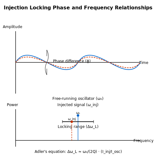
Advanced techniques like sub-sampling phase-locked loops (SSPLLs) and injection locking are used to improve performance in RF systems. Recent research focuses on optoelectronic oscillators achieving ultra-low phase noise through optical delay lines with Q factors exceeding 109.
Voltage-Controlled Oscillators (VCOs)
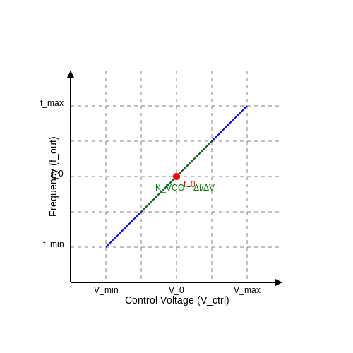
Voltage-controlled oscillators (VCOs) are critical components in RF signal generation, providing tunable frequency output as a function of an applied control voltage. Their operation hinges on the principle of voltage-dependent reactance modulation, typically achieved through varactor diodes or transistor-based tuning networks.
Core Operating Principle
The fundamental relationship governing a VCO's output frequency f is:
where f0 is the center frequency, KVCO is the tuning sensitivity (in Hz/V), and Vctrl is the control voltage. This linear approximation holds for small tuning ranges; in practice, the KVCO exhibits nonlinearity across wider ranges.
Varactor-Based Tuning
The most common implementation uses reverse-biased varactor diodes whose junction capacitance varies with applied voltage:
where Cj0 is the zero-bias capacitance, φ is the built-in potential (~0.7V for Si), and γ is the grading coefficient (0.5 for abrupt junctions). This capacitance modulates the resonant tank frequency in LC oscillators:
Phase Noise Considerations
VCO phase noise follows Leeson's model, with close-in noise dominated by upconverted 1/f noise:
where F is the noise factor, Q is the tank quality factor, and fc is the 1/f corner frequency. High-Q resonators (e.g., ceramic or cavity-based) achieve sub-100 dBc/Hz noise at 100 kHz offset in the GHz range.
Modern Implementations
Contemporary designs employ:
- Cross-coupled LC topologies for differential operation and improved common-mode rejection
- Switched capacitor banks for discrete coarse tuning alongside varactor fine tuning
- Digital calibration loops to compensate for process-voltage-temperature variations
Advanced MMIC VCOs in SiGe or GaAs technologies achieve tuning ranges exceeding 50% with phase noise below -110 dBc/Hz at 1 MHz offset in the 6-40 GHz range, critical for 5G and satellite communications.
Phase-Locked Loops (PLLs) in RF Generation
Fundamental Operation of PLLs
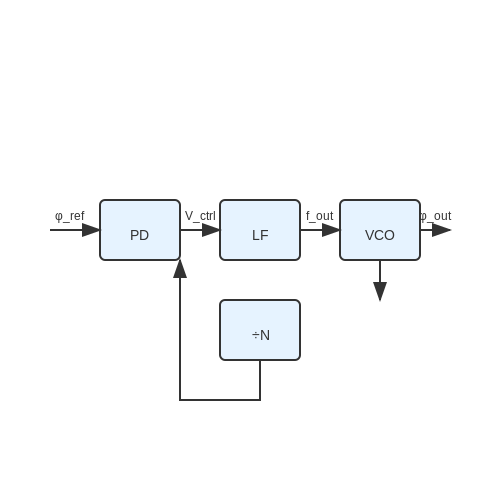
A phase-locked loop (PLL) is a feedback control system that generates an output signal whose phase is locked to the phase of an input reference signal. The core components include:
- Phase detector (PD): Compares phase difference between reference and feedback signals
- Loop filter (LF): Removes high-frequency components from PD output
- Voltage-controlled oscillator (VCO): Generates output signal with frequency proportional to control voltage
- Frequency divider (÷N): Optional divider in feedback path for frequency synthesis
where \( \phi_{out} \) is the output phase, \( K_{vco} \) is the VCO gain (rad/s/V), and \( V_{ctrl} \) is the control voltage.
Phase Noise Considerations
Phase noise in PLLs follows Leeson's model, with the single-sideband phase noise spectral density given by:
where \( f_m \) is the offset frequency, \( F \) is the noise figure, \( Q_L \) is the loaded Q-factor, and \( f_c \) is the flicker noise corner frequency.
Integer-N vs. Fractional-N PLLs
| Parameter | Integer-N | Fractional-N |
|---|---|---|
| Frequency Resolution | Limited to reference frequency | Sub-Hertz possible |
| Phase Noise | Better close-in phase noise | Higher due to ΣΔ modulation |
| Spurious Content | Reference spurs only | Fractional spurs present |
Modern PLL Architectures
Advanced PLL designs address traditional limitations:
- Digital PLLs (DPLLs): Replace analog components with digital equivalents for better programmability
- All-digital PLLs (ADPLLs): Utilize time-to-digital converters (TDCs) for phase detection
- Sub-sampling PLLs: Sample VCO output directly to reduce phase noise
Practical Implementation Challenges
Key design considerations for RF PLLs include:
- VCO pulling effects in integrated designs
- Power supply noise sensitivity
- Reference spur suppression techniques
- Loop bandwidth optimization for phase noise and settling time tradeoffs
where \( \omega_{3dB} \) is the loop bandwidth, \( \omega_n \) is the natural frequency, and \( \omega_z \) is the zero frequency.
3. Direct Digital Synthesis (DDS) Principles
Direct Digital Synthesis (DDS) Principles
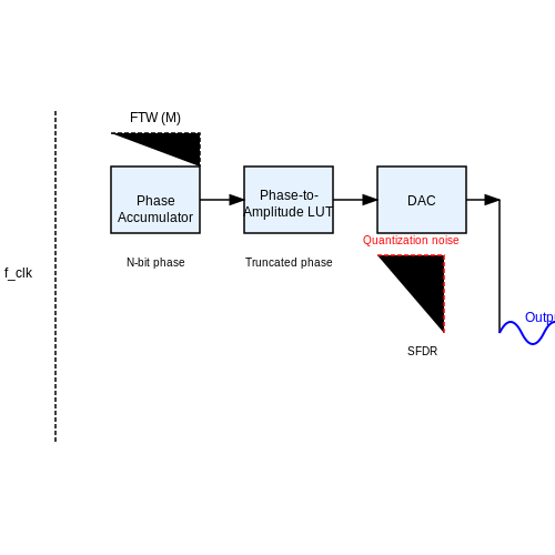
Direct Digital Synthesis (DDS) is a method of generating precise, frequency-agile waveforms using digital signal processing techniques. At its core, a DDS system consists of a phase accumulator, a phase-to-amplitude converter (typically implemented via a lookup table), and a digital-to-analog converter (DAC). The phase accumulator increments a digital phase value at each clock cycle, and the phase-to-amplitude converter maps this phase to a corresponding amplitude value stored in memory.
Phase Accumulator and Frequency Tuning
The phase accumulator is a critical component that determines the output frequency. It operates by adding a frequency tuning word (FTW) to the current phase value at each clock cycle. The output frequency fout is given by:
where M is the frequency tuning word, fclk is the clock frequency, and N is the bit width of the phase accumulator. The frequency resolution Δf is:
For example, a 32-bit phase accumulator with a 100 MHz clock yields a frequency resolution of approximately 0.023 Hz, enabling extremely fine-grained frequency control.
Phase-to-Amplitude Conversion
The phase accumulator's output is truncated to a lower bit width (e.g., 12 bits) to address a lookup table (LUT) storing amplitude values for the desired waveform (sine, square, triangle, etc.). The LUT output is then fed to a DAC for analog conversion. The truncation introduces phase quantization noise, which can be mitigated by phase dithering or increasing the LUT size.
Spurious Signals and Noise Considerations
DDS systems are susceptible to spurious signals due to phase truncation, amplitude quantization, and DAC nonlinearities. The spurious-free dynamic range (SFDR) is a key performance metric. The worst-case spur level Lspur due to phase truncation is approximated by:
where P is the number of phase bits retained after truncation. High-performance DDS systems employ ΣΔ modulation or noise shaping to push quantization noise out of the band of interest.
Applications and Practical Implementations
DDS is widely used in:
- Communications systems for agile local oscillators and modulation.
- Radar and sonar for frequency-hopping and chirp generation.
- Test equipment such as arbitrary waveform generators.
Modern integrated DDS solutions (e.g., Analog Devices AD9910) combine high-speed DACs with advanced features like linear frequency sweeping and programmable modulation profiles.
3.2 Digital-to-Analog Converters (DACs) in RF Generation
Fundamentals of DAC Operation
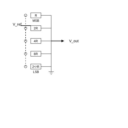
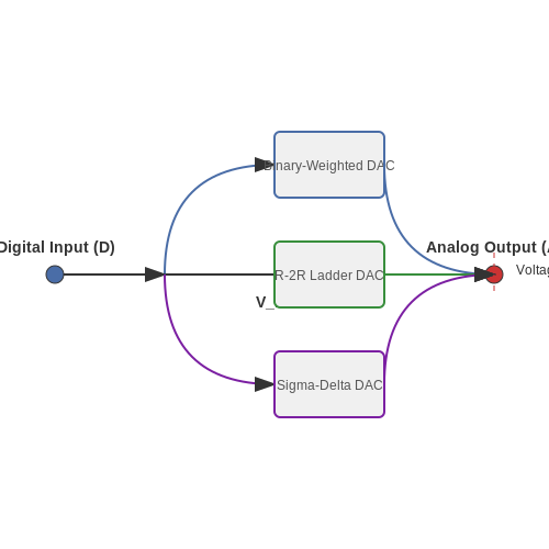
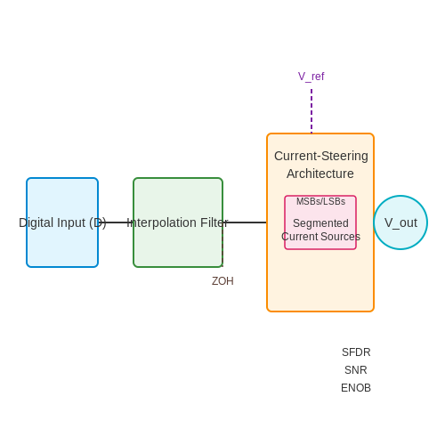
Digital-to-Analog Converters (DACs) transform discrete digital signals into continuous analog waveforms, a critical function in RF signal synthesis. The conversion process involves reconstructing a sampled signal using a zero-order hold (ZOH) or interpolation filters. The output voltage \( V_{out} \) of an N-bit DAC is given by:
where \( D \) is the digital input code, \( V_{ref} \) is the reference voltage, and \( N \) is the resolution in bits. High-speed DACs leverage current-steering architectures to achieve sampling rates exceeding 10 GS/s, essential for millimeter-wave applications.
Key Performance Metrics
The fidelity of RF generation depends on DAC specifications:
- Spurious-Free Dynamic Range (SFDR): Measures the worst-case harmonic or non-harmonic distortion relative to the carrier.
- Signal-to-Noise Ratio (SNR): Quantifies noise power within the Nyquist bandwidth.
- Effective Number of Bits (ENOB): Derives usable resolution after accounting for noise and distortion.
For a DAC with quantization noise \( Q_n \), SNR is theoretically bounded by:
Advanced Architectures for RF Applications
Modern RF DACs employ:
- Segmented Current Sources: Reduces glitch energy by splitting MSBs and LSBs into separate switching networks.
- Return-to-Zero (RZ) Outputs: Minimizes inter-symbol interference in multi-carrier systems.
- Direct Digital Synthesis (DDS): Combines DACs with NCOs (Numerically Controlled Oscillators) for agile frequency tuning.
Jitter and Phase Noise Considerations
Clock jitter \( t_j \) directly impacts phase noise \( \mathcal{L}(f) \) in synthesized RF signals. The relationship is approximated by:
where \( f_0 \) is the output frequency. Sub-picosecond jitter is mandatory for 5G NR and radar systems.
Case Study: Wideband OFDM Generation
In a 5G testbed, a 14-bit, 12 GS/s DAC generates 800 MHz OFDM channels. Digital pre-distortion compensates for the DAC’s nonlinear transfer function, achieving < 0.1% EVM at 28 GHz after upconversion.
3.3 Software-Defined Radio (SDR) Techniques
Modern SDR systems leverage reconfigurable hardware and software to achieve flexible RF signal generation, replacing traditional analog components with digital signal processing (DSP). The core principle involves converting analog signals to digital representations early in the signal chain, enabling programmable modulation, filtering, and frequency agility.
Architecture and Key Components
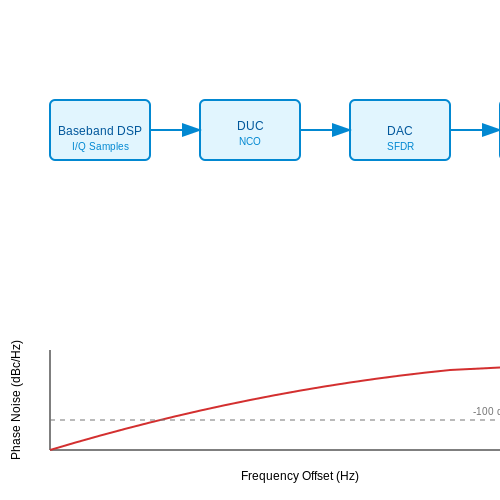
A typical SDR transmitter consists of:
- Digital Baseband Processor: Implements modulation schemes (e.g., QAM, OFDM) in software.
- Digital Upconverter (DUC): Translates baseband signals to intermediate frequencies (IF) using numerically controlled oscillators (NCOs).
- Digital-to-Analog Converter (DAC): Converts digital waveforms to analog signals with sufficient resolution (typically 12-16 bits).
- RF Frontend: Includes mixers, amplifiers, and filters for final frequency translation and power amplification.
Mathematical Foundation
The digital upconversion process can be modeled as:
where I[n] and Q[n] are the in-phase and quadrature baseband samples, fIF is the intermediate frequency, and Ts is the sampling period. The equivalent analog signal after DAC conversion is:
Practical Implementation Considerations
Key challenges in SDR signal generation include:
1. Spectral Purity
Spurious emissions arise from DAC nonlinearities and clock jitter. The spurious-free dynamic range (SFDR) is given by:
where N is the DAC resolution in bits and DNLrms is the differential nonlinearity.
2. Phase Noise
Local oscillator phase noise impacts modulation accuracy. For a PLL-based synthesizer, the single-sideband phase noise £(f) follows:
where F is the noise figure, QL is the loaded Q-factor, and f0 is the carrier frequency.
Advanced Techniques
State-of-the-art SDR systems employ:
- Direct Digital Synthesis (DDS): Achieves sub-Hz frequency resolution through phase accumulation and lookup tables.
- Adaptive Predistortion: Compensates for power amplifier nonlinearities using real-time feedback loops.
- Multicarrier Generation: Enables concurrent transmission of multiple standards (e.g., 5G NR and WiFi 6) through polyphase filter banks.
4. Frequency Multiplication and Division
4.1 Frequency Multiplication and Division
Frequency Multiplication
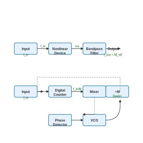
Frequency multiplication is the process of generating an output signal whose frequency is an integer multiple of the input frequency. This is achieved using nonlinear devices or phase-locked loops (PLLs). The most common nonlinear devices used are varactor diodes and step-recovery diodes, which generate harmonics of the input signal.
For a sinusoidal input signal vin(t) = A sin(ωt), passing it through a nonlinear device produces an output containing harmonics:
where kn are coefficients determined by the nonlinearity. A bandpass filter then selects the desired harmonic nω.
In PLL-based multiplication, a voltage-controlled oscillator (VCO) is locked to a multiple of the reference frequency using a frequency divider in the feedback path. The output frequency is given by:
where N is the multiplication factor.
Frequency Division
Frequency division produces an output signal whose frequency is a submultiple of the input frequency. This is commonly implemented using digital counters or regenerative frequency dividers.
A synchronous counter divides the input frequency by M by toggling its output every M input cycles. The output frequency is:
Regenerative dividers use mixing and filtering to achieve division. The input signal fin is mixed with the divided output fout = fin/M to produce sum and difference frequencies. A filter selects fin - fout, which is fed back to maintain oscillation at the divided frequency.
Practical Considerations
Phase noise is a critical parameter in frequency multiplication and division. Multiplication increases phase noise by 20log10(N), while division reduces it by 20log10(M). Spurs and harmonics must be carefully managed through filtering and proper loop bandwidth design in PLL implementations.
Modern frequency synthesizers often combine both techniques, using a high-frequency VCO with division to achieve precise, low-noise output frequencies across wide ranges. Fractional-N synthesis further enhances resolution by dynamically varying the division ratio.
4.2 Mixers and Frequency Translation
Fundamental Principles of Mixers
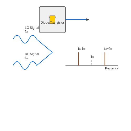
Mixers are nonlinear devices used to translate signals from one frequency to another by exploiting the mathematical property of multiplication in the time domain. Given two input signals, fLO (Local Oscillator) and fRF (Radio Frequency), the mixer produces sum and difference frequencies:
This process is governed by the trigonometric identity for multiplication of sinusoidal signals:
In practical implementations, mixers are designed to suppress unwanted harmonics and spurious responses, with performance characterized by conversion loss, isolation, and intermodulation distortion.
Types of Mixers
Mixers can be categorized based on their circuit topology and nonlinear element:
- Diode Mixers: Utilize the nonlinear I-V characteristic of diodes, commonly in ring or star configurations for balanced operation.
- Active Mixers: Employ transistors (FETs or BJTs) to provide conversion gain rather than loss.
- Gilbert Cell Mixers: A double-balanced active mixer topology offering high linearity and port isolation, widely used in IC designs.
Balanced mixers (single or double-balanced) are preferred in RF systems due to their ability to reject LO noise and even-order harmonics.
Frequency Translation in Practice
Frequency translation is essential in:
- Superheterodyne Receivers: Downconverting RF signals to a fixed intermediate frequency (IF) for amplification and filtering.
- Upconverters in Transmitters: Shifting baseband signals to the desired RF carrier frequency.
- Software-Defined Radios (SDR): Enabling flexible frequency agility through digital mixing techniques.
Image rejection mixers (e.g., Hartley or Weaver architectures) are used to mitigate the problem of image frequencies in heterodyne systems.
Nonlinearity and Intermodulation
Mixers inherently introduce nonlinear effects, leading to intermodulation products. For two-tone inputs at f1 and f2, the output includes:
Third-order intercept point (IP3) is a critical metric for evaluating mixer linearity, defined as the theoretical input power where third-order products equal the fundamental tones.
Phase Noise Considerations
Local oscillator phase noise directly impacts mixer performance, introducing jitter in the translated signal. The phase noise profile of the LO is convolved with the input signal, affecting receiver sensitivity and transmitter spectral purity.
Low-noise oscillators and careful layout techniques are necessary to minimize phase noise contributions in frequency translation systems.
Noise Reduction and Signal Purity
Phase Noise and Its Impact on RF Signals
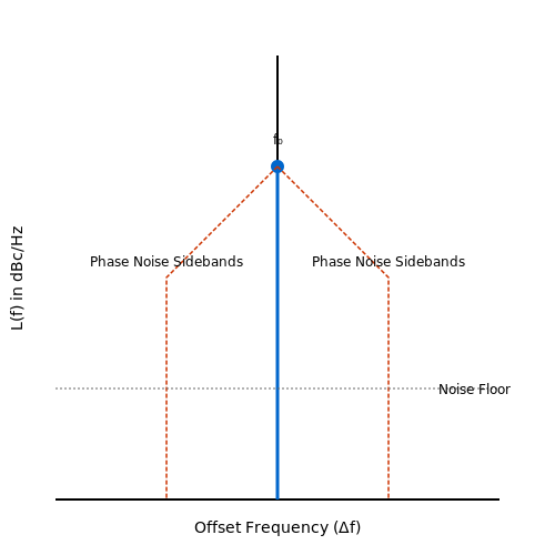
Phase noise, represented as L(f), quantifies the short-term random fluctuations in the phase of an oscillator's output signal. It is typically measured in dBc/Hz and degrades signal purity, leading to increased bit error rates (BER) in communication systems. The phase noise power spectral density (PSD) is derived from the Leeson model:
where F is the noise figure, k is Boltzmann’s constant, T is temperature, Psig is the signal power, f0 is the carrier frequency, QL is the loaded Q-factor, and fc is the flicker noise corner frequency. Lower phase noise is critical for high-order modulation schemes like 64-QAM.
Techniques for Phase Noise Reduction
- High-Q Resonators: Dielectric resonators or sapphire-loaded cavities improve QL, reducing the f0/2QL term in the Leeson equation.
- Active Noise Cancellation: Feedforward or feedback systems inject anti-phase noise to cancel oscillator phase noise.
- Low-Noise Amplifiers (LNAs): Minimize additive noise in signal chains, particularly in receiver front-ends.
Spurious Suppression Methods
Spurious tones, caused by power supply harmonics or mixer nonlinearities, are quantified as dBc below the carrier. Key mitigation strategies include:
- Filtering: Bandpass filters (BPFs) with sharp roll-off (e.g., Chebyshev or elliptic) attenuate out-of-band spurs.
- Linearization: Predistortion or feedforward techniques compensate for amplifier nonlinearities.
- Grounding and Shielding: Reduce conducted/radiated interference via multilayer PCBs and RF shielding cans.
Case Study: Low-Noise Synthesizer Design
A 10 GHz PLL-based synthesizer achieving −110 dBc/Hz phase noise at 100 kHz offset requires:
- A voltage-controlled oscillator (VCO) with QL > 200.
- A fractional-N divider with sigma-delta modulation to suppress quantization noise.
- Active loop bandwidth optimization to balance reference noise and VCO noise.
Advanced Topics: Cryogenic Cooling
For ultra-low-noise applications (e.g., radio astronomy), cooling oscillators to 4 K reduces thermal noise by a factor of:
This technique has enabled phase noise below −150 dBc/Hz in superconducting resonators.
5. RF Signal Generation in Wireless Communication
RF Signal Generation in Wireless Communication
Fundamentals of RF Signal Generation
Radio frequency (RF) signal generation is the process of creating high-frequency electromagnetic waveforms for wireless communication systems. The key parameters of an RF signal—frequency, amplitude, phase, and modulation—must be precisely controlled to ensure reliable transmission and reception. The most common methods for generating RF signals include:
- Direct synthesis using voltage-controlled oscillators (VCOs)
- Phase-locked loops (PLLs) for frequency stabilization
- Direct digital synthesis (DDS) for programmable waveform generation
- Frequency multiplication of lower-frequency sources
Voltage-Controlled Oscillators (VCOs)
A VCO generates an output signal whose frequency is controlled by an input voltage. The relationship between the control voltage Vctrl and the output frequency fout is given by:
where f0 is the center frequency and KVCO is the tuning sensitivity in Hz/V. Modern VCOs achieve phase noise performance better than -110 dBc/Hz at 100 kHz offset for frequencies up to 6 GHz.
Phase-Locked Loop (PLL) Synthesis
PLLs provide stable frequency synthesis by comparing the phase of a VCO output to a reference oscillator. The basic PLL components are:
The output frequency is locked to the reference according to:
where N is the divider ratio. Fractional-N PLLs enable finer frequency resolution by dynamically changing N.
Direct Digital Synthesis (DDS)
DDS systems generate waveforms digitally using a phase accumulator and look-up table. The output frequency is determined by:
where M is the phase increment, n is the accumulator bit width, and fclock is the system clock frequency. Modern DDS chips like the AD9910 achieve 1 GHz output with 32-bit frequency tuning resolution.
Frequency Multiplication Techniques
Frequency multipliers use nonlinear devices to generate harmonics of a fundamental signal. The output power at the nth harmonic is given by:
where ηn is the conversion efficiency for the nth harmonic. Practical multipliers using step-recovery diodes or transistor-based designs achieve conversion efficiencies of 10-30% for 2× to 4× multiplication.
Modulation Implementation
Modern wireless systems employ complex modulation schemes like QAM and OFDM. The baseband signal s(t) modulates the RF carrier through:
where A(t) and ϕ(t) carry the amplitude and phase information respectively. I/Q modulators implement this using two mixers driven by quadrature carriers:
This approach enables efficient generation of complex modulation formats with precise control over both amplitude and phase.
5.2 Radar and Satellite Applications
Radar and satellite systems rely on precise RF signal generation to achieve high-resolution detection, ranging, and communication. The fundamental requirement is generating stable, high-power signals with minimal phase noise, often at microwave and millimeter-wave frequencies. Key techniques include direct synthesis, phase-locked loops (PLLs), and direct digital synthesis (DDS), each optimized for specific performance trade-offs.
Frequency Stability and Phase Noise
In radar applications, phase noise directly impacts target detection sensitivity. The Leeson model describes phase noise (L(f)) in oscillators:
where F is the noise figure, k is Boltzmann’s constant, T is temperature, Psig is the signal power, f0 is the carrier frequency, QL is the loaded Q-factor, and fc is the flicker noise corner frequency. Satellite transponders demand ultra-low phase noise (e.g., <−110 dBc/Hz at 1 kHz offset) to maintain link budget margins.
Pulsed Radar Signal Generation
Pulsed radars modulate RF carriers with high-power pulses (µs to ms durations). The pulse repetition frequency (PRF) and duty cycle are critical:
where Tp is the pulse period and τ is the pulse width. Modern systems use GaN-based power amplifiers to achieve peak powers exceeding 1 kW at X-band frequencies.
Satellite Communication Modulations
Geostationary satellites employ complex modulations like QPSK, 8PSK, or 16APSK to maximize spectral efficiency. The Shannon-Hartley theorem bounds the achievable data rate:
where C is channel capacity (bps), B is bandwidth (Hz), and S/N is the signal-to-noise ratio. Forward error correction (FEC) codes (e.g., LDPC, Turbo) are applied to operate near this limit.
Beamforming and Phased Arrays
Active electronically scanned arrays (AESAs) use phase shifters to steer beams without mechanical movement. The array factor for N elements spaced by d is:
where wn are complex weights and k is the wavenumber. Digital beamforming in satellite payloads enables dynamic coverage reconfiguration.
Case Study: Synthetic Aperture Radar (SAR)
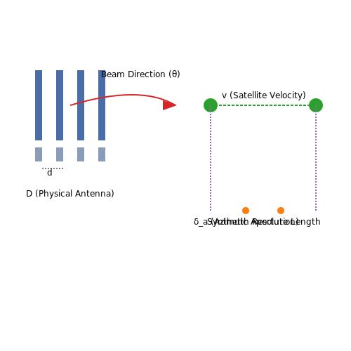
SAR achieves sub-meter resolution by coherently integrating radar returns over a synthetic aperture. The azimuth resolution (δa) is:
where D is the physical antenna length, independent of range. LEO satellites like TerraSAR-X use this technique with chirp bandwidths >150 MHz.
5.3 Test and Measurement Equipment
Accurate RF signal generation demands precise instrumentation to validate frequency, power, modulation, and spectral purity. The following equipment is indispensable for characterizing and troubleshooting RF systems.
Signal Generators
Modern vector signal generators (VSGs) synthesize complex modulated waveforms with programmable parameters such as frequency, amplitude, and phase noise. Key specifications include:
- Frequency range: Determines the upper and lower bounds of operation (e.g., 9 kHz–44 GHz for millimeter-wave applications).
- Phase noise: Critical for coherent systems, typically specified in dBc/Hz at a given offset (e.g., −110 dBc/Hz at 10 kHz offset).
- Modulation bandwidth: Defines the maximum instantaneous bandwidth for waveforms like OFDM or QAM.
Spectrum Analyzers
Spectrum analyzers measure frequency-domain characteristics, including harmonics, spurs, and noise floor. A real-time spectrum analyzer (RTSA) captures transient signals using fast Fourier transforms (FFT). The noise floor is governed by:
where k is Boltzmann’s constant, T is temperature, B is bandwidth, and NF is the analyzer’s noise figure.
Network Analyzers
Vector network analyzers (VNAs) characterize S-parameters of RF components. Calibration using SOLT (Short-Open-Load-Thru) standards minimizes systematic errors. The reflection coefficient (Γ) is derived from:
Power Meters
Thermistor-based or diode-detector power meters measure average RF power with traceable accuracy. For pulsed signals, peak power sensors integrate over the pulse width:
where DC is the duty cycle.
Oscilloscopes
High-bandwidth (>20 GHz) oscilloscopes with time-domain reflectometry (TDR) capture transient effects in RF circuits. Eye diagrams assess signal integrity in digital modulation schemes.
Phase Noise Analyzers
Specialized instruments measure phase fluctuations using cross-correlation techniques to suppress instrument noise. The Allan deviation provides time-domain stability metrics.
Practical Considerations
Impedance matching (50 Ω or 75 Ω) minimizes reflections. For millimeter-wave frequencies, waveguide interfaces and calibration kits are essential. Automated test systems leverage GPIB or PXI interfaces for scripted measurements.
6. Key Textbooks and Research Papers
6.1 Key Textbooks and Research Papers
- RF CIRCUIT DESIGN - Wiley Online Library — 1 DIFFERENCE BETWEEN RF AND DIGITAL CIRCUIT DESIGN 3 1.1 Controversy 3 1.1.1 Impedance Matching 4 1.1.2 Key Parameter 5 1.1.3 Circuit Testing and Main Test Equipment 6 1.2 Difference of RF and Digital Block in a Communication System 6 1.2.1 Impedance 6 1.2.2 Current Drain 7 1.2.3 Location 7 1.3 Conclusions 9 1.4 Notes for High-Speed Digital ...
- INTRODUCTION TO RF PROPAGATION - Wiley Online Library — 1.2.2.1 Indirect or Obstructed Propagation 6 1.2.2.2 Tropospheric Propagation 6 1.2.2.3 Ionospheric Propagation 6 1.2.3 Propagation Effects as a Function of Frequency 9 1.3 Why Model Propagation? 10 1.4 Model Selection and Application 11 1.4.1 Model Sources 11 1.5 Summary 12 References 12 Exercises 13 2. Electromagnetics and RF Propagation 14 2 ...
- PDF RF Microelectronics - pearsoncmg.com — 3.3.2 Signal Constellations 105 3.3.3 Quadrature Modulation 107 3.3.4 GMSK and GFSK Modulation 112 3.3.5 Quadrature Amplitude Modulation 114 3.3.6 Orthogonal Frequency Division Multiplexing 115 3.4 Spectral Regrowth 118 3.5 Mobile RF Communications 119 3.6 Multiple Access Techniques 123 3.6.1 Time and Frequency Division Duplexing 123
- PDF Radio-Frequency Electronics - Cambridge University Press & Assessment — 1.1 RF circuits 2 1.2 Narrowband nature of RF signals 3 1.3 AC circuit analysis a brief review 3 1.4 Impedance and admittance 4 1.5 Series resonance 4 1.6 Parallel resonance 5 1.7 Nonlinear circuits 5 Problems 5 2 Impedance matching 10 2.1 Transformer matching 11 2.2 L-networks 12 2.3 Higher Q pi and T-networks 14 2.4 Lower Q the double L ...
- PDF Radio Frequency Integrated Circuits and Systems — 5.3 Small signal non-linearity 163 5.4 Large signal non-linearity 177 5.5 Reciprocal mixing 179 5.6 Harmonic mixing 182 5.7 Transmitter concerns 184 5.8 Problems 201 5.9 References 202 6 Low-noise amplifiers 203 6.1 Matching requirements 204 6.2 RF tuned amplifiers 208 6.3 Shunt feedback LNAs 216 6.4 Series feedback LNAs 220 6.5 Feedforward ...
- PDF An Introduction to Radio Frequency Engineering — 1.5 Circuit model of a transmit system. 6 1.6 Conventions for effective length. 6 1.7 A dipole antenna used to collect energy from an electromagnetic wave. 7 1.8 Circuit model of receive system. 7 1.9 Reciprocity principle. 8 1.10 Transmit/receive system. 8 1.11 Noise sources. 9 1.12 Typical antenna noise temperatures for a dipole and a variety of
- Multiband RF Circuits and Techniques for Wireless Transmitters — 2014 IEEE International Conference on Acoustics, Speech and Signal Processing (ICASSP), 2014. Some recently developed 0.18-µm SiGe BiCMOS radiofrequency integrated circuits (RFICs) for multiband multimode wireless communications, radar and sensing systems, which provides many benefits for sensing and communications in uncertain environments with harsh operational scenarios, are presented.
- RF Channelization Technology - SpringerLink — Pure channelization is implemented in a hierarchical manner, as shown in Fig. 6.3; that is, a multi-level frequency splitter is used to convert the broadband signal multiple times to change the RF signal into multiple signals with the same intermediate frequency and bandwidth. Then perform signal detection on each signal to obtain the frequency ...
- PDF Rf System Design of Transceivers for Wireless Communications — electronic adaptation, computer software, or by similar or dissimilar methodology now ... 6 1.3. Organization of This Book ... has a good RF background, basic knowledge of signal and communication theory, and fundamentals of analog and mixed signal circuits. Completion of this book is the result of helps and encouragement
- PDF Chapter 6 Transceiver I: Transmitter Architectures - Springer — The modulated IF signal is further up-converted into the RF frequency with the second local oscillator (LO2). The first bandpass filter (BPF) suppresses the harmonics of the IF signal, while the second BPF passes the wanted RF signal at the frequency of either ω 2 ω 1 or ω 2+ω 1 depending on the application and attenuates the harmonics of ...
6.2 Online Resources and Tutorials
- PDF Software-Defined Radio for Engineers - Analog — 2.6 Digital Signal Processing Techniques for SDR 61 2.6.1 Discrete Convolution 61 2.6.2 Correlation 65 2.6.3 Z-Transform 66 2.6.4 Digital Filtering 69 2.7 Transmit Techniques for SDR 73 2.7.1 Analog Reconstruction Filters 75 2.7.2 DACs 76 2.7.3 Digital Pulse-Shaping Filters 78 2.7.4 Nyquist Pulse-Shaping Theory 79 2.7.5 Two Nyquist Pulses 81
- PDF RF Microelectronics - pearsoncmg.com — 3.3.2 Signal Constellations 105 3.3.3 Quadrature Modulation 107 3.3.4 GMSK and GFSK Modulation 112 3.3.5 Quadrature Amplitude Modulation 114 3.3.6 Orthogonal Frequency Division Multiplexing 115 3.4 Spectral Regrowth 118 3.5 Mobile RF Communications 119 3.6 Multiple Access Techniques 123 3.6.1 Time and Frequency Division Duplexing 123
- RF Education and Teaching - Tektronix — TSG4100A Series RF Vector Signal Generators offer mid-range RF performance and up to 200MHz modulation bandwidth. Convenient, in-field software upgrades easily transition units from analog to more advanced vector and digital modulation capabilities, providing the most flexible configuration and best CAPEX protection. Learn More »
- PDF Channels, modulation, and demodulation - MIT OpenCourseWare — In other words, the signal points are the same as the representation points of a symmetric M-point uniform scalar quantizer. a 1 a 2 a 3 a 4 a 5 a 6 a 7 a 8 d 0 Figure 6.2: An 8-PAM signal set. If the incoming bits are independent equiprobable random symbols (which is well approximated by effective source coding), then each signal u
- PDF An Introduction to Radio Frequency Engineering — RF systems, circuit design, antennas, propagation and digital techniques. Written for upper-level undergraduate courses, it will also provide an excellent introduction to the subject for graduate students, researchers and practising engineers. CHRISTOPHER COLEMAN is an associate professor of electrical and electronic engineering at the
- PDF GUIDE TO RF SIGNALS - Tektronix — The first step in identifying a radio signal is to determine the operating frequency of the transmitter. Other than Industrial/Scientific/Medical bands, the radio spectrum is a tightly managed resource. When we are trying to determine what type of signal we are seeing, we need to first identify the operating frequency. A simple technique is to
- PDF The Essential Signal Generator Guide - Keysight — requirement, you need the right signal generator. The frequency spectrum is a finite resource. Complex modulation schemes increase spectral efficiency, enabling far higher data rates. Unfortunately, complex modulation schemes depend on accurate and stable signal generators to work effectively. With all the specifications and features
- eGuide to RF Signals - Tektronix — The first step in identifying a radio signal is to determine the operating frequency of the transmitter. Other than Industrial/Scientific/Medical bands, the radio spectrum is a tightly managed resource. When we are trying to determine what type of signal we are seeing, we need to first identify the operating frequency.
- 6.02 Tutorial 1 | Introduction to EECS II: Digital Communication ... — This resource contains information regarding tutorial 1. Browse Course Material Syllabus ... Signal Processing; Telecommunications; Learning Resource Types assignment Problem Sets. grading Exams. ... This resource contains information regarding tutorial 1. Resource Type: Tutorials. pdf.
- Introduction to EECS II: Digital Communication Systems | Electrical ... — An introduction to several fundamental ideas in electrical engineering and computer science, using digital communication systems as the vehicle. The three parts of the course—bits, signals, and packets—cover three corresponding layers of abstraction that form the basis of communication systems like the Internet. The course teaches ideas that are useful in other parts of EECS: abstraction ...
6.3 Industry Standards and Datasheets
- PDF 6 GHz RF Vector Signal Transceiver (VST) - VIAVI Solutions Inc. — Software Analysis/Generation (optional) The VST is a software-designed instrument with software analysis and generation packages for the latest cellular, connectivity and IoT standards. Expanded Bandwidth (option 02) The VST module provides an industry leading 200 MHz of RF bandwidth leveraging the speed and flexibility of the user programmable ...
- PDF Modulation and Signal Generation with R&S® Signal Generators — The following section of this educational note provides a closer look at RF signal generators (analog, vector-modulated) and at arbitrary waveform generators. 1.2.1 Analog Signal Generators With analog signal generators, the focus is on producing a high-quality RF signal. They provide support for the analog modulation modes AM / FM and φM.
- Modulation and Signal Generation with R&S®Signal Generators — To permit a better understanding of the specifications found on data sheets, a closer look at the most important parameters for a signal generator is provided. Beyond the output of spectrally pure signals, a key function of RF signal generators is the generation of analog- and digitally modulated signals.
- FSW | Brochure and Datasheet | Rohde & Schwarz — Rohde & Schwarz has signal generation and analysis solutions that cover millimeterwave frequencies and beyond. Our signal generation and analysis solution portfolio addresses the bandwidth and frequency requirements for 5G and beyond, offering a wide range of features and application software for any testing challenge.
- PDF Instrument Fundamentals: Signal Generator Basics - Rohde & Schwarz — What is a signal generator. 3 Instrument Fundamentals: Signal Generator Basics Signal generators play a vital role in test and measurement. Generate test signals when applied to components such as filters, amplifier or entire modules. Determine the component's behavior and characteristics. Beyond the output of spectrally pure signals. −Key functions are analog and digitally modulated signals.
- PSG Signal Generators - Keysight — PathWave Signal Generation software is a flexible suite of signal creation tools that will reduce the time you spend on signal simulation. ... Learn how to set up an RF signal generator for a carrier signal and optimize the noise settings. ... which may be useful in the application of the product. Unless otherwise noted, this data sheet applies ...
- PDF The Essential Signal Generator Guide - Keysight — the I and Q signals orthogonal to each other so that they do not interfere with each other. Figure 5.2. Baseband IQ modulation To learn more about the basics of digital modulation, refer to Digital Modulation in Communications Systems. Q 90-degree phase shift Composite output signal LO (carrier freq.) I Σ The Essential Signal Generator Guide | 6
- PDF The Essential Signal Generator Guide Building a Solid Foundation in RF ... — Choosing the right signal generator is essential for obtaining trustworthy test results and accelerating time-to-market. This paper covers the basic functionalities, types, and key specifications of signal generators in detail. Signal generators are crucial in eliminating uncertainties in test results for engineers working on consumer electronics, wireless communications, or radar devices ...
- PDF RF Basics Design Guide - Microchip Technology — prohibitively expensive including the industry's most cost-sensitive consumer products. Increased integration, along with vastly im-proved development tools, has helped to ease the burden on the RF designer and sustained innovation continues to reduce time to market. For Micrel RF products, this translates into a nearly drop-in