Low-Frequency Signal Conditioning
1. Characteristics of Low-Frequency Signals
Characteristics of Low-Frequency Signals
Definition and Frequency Range
Low-frequency signals are typically defined as those with frequencies below 300 kHz, though the exact boundary can vary depending on the application. In power systems, for instance, 50 Hz or 60 Hz signals are considered low-frequency, while in biomedical applications, signals below 1 kHz (such as EEG or ECG waveforms) fall into this category. The defining characteristic is that these signals exhibit minimal skin effect in conductors and negligible radiative losses compared to higher-frequency signals.
Time-Domain Behavior
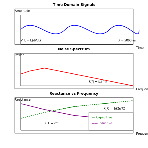
Low-frequency signals maintain quasi-static field behavior, meaning their wavelength is significantly larger than the physical dimensions of typical circuits. For a 60 Hz signal in air:
This results in nearly instantaneous propagation of electric and magnetic fields across circuit elements. The voltage-current relationship in passive components follows standard constitutive equations without significant phase delay:
Noise Susceptibility
Low-frequency signals are particularly vulnerable to 1/f (pink) noise and DC drift. The noise power spectral density follows:
where K is a constant specific to the device. This makes signal conditioning challenging below 10 Hz, requiring techniques like chopper stabilization or auto-zeroing in amplifier designs.
Impedance Considerations
At low frequencies, capacitive and inductive reactances become significant:
For a 1 μF capacitor at 10 Hz, the reactance is approximately 15.9 kΩ, making passive filtering impractical without extremely large component values. This necessitates active filtering approaches in most practical designs.
Practical Measurement Challenges
When measuring low-frequency signals, several artifacts become prominent:
- Electrode polarization: DC offsets up to hundreds of millivolts in biopotential measurements
- Thermoelectric effects: Microvolt-level signals corrupted by junction temperature differences
- Triboelectric noise: Cable movement generating spurious low-frequency components
Signal Conditioning Requirements
Effective conditioning of low-frequency signals demands:
- High input impedance (>1 GΩ) to prevent loading effects
- Ultra-low bias current (<1 pA) amplifiers
- Precision DC restoration circuits
- Multi-pole active filters with sharp roll-off characteristics
Modern implementations often use instrumentation amplifiers with correlated double sampling techniques to achieve input-referred offsets below 1 μV.
1.2 Common Sources of Low-Frequency Noise
Thermal (Johnson-Nyquist) Noise
Thermal noise arises due to the random motion of charge carriers in resistive materials, governed by the fluctuation-dissipation theorem. The power spectral density (PSD) of thermal noise is frequency-independent (white noise) but manifests as a dominant low-frequency contributor when integrated over bandwidth. The RMS voltage noise is given by:
where k is Boltzmann's constant (1.38×10⁻²³ J/K), T is absolute temperature, R is resistance, and B is bandwidth. At 1 kΩ and 300 K, this produces ~4 nV/√Hz. In low-frequency applications (<1 kHz), the integrated noise becomes significant due to the 1/f characteristics of subsequent amplification stages.
Flicker (1/f) Noise
Flicker noise dominates at frequencies below ~100 Hz in semiconductor devices and resistors. Its PSD follows:
where Kf is a device-specific constant and α typically ranges from 0.8 to 1.3. In MOSFETs, this arises from carrier trapping at oxide interfaces, with corner frequencies (where 1/f noise equals white noise) reaching 10 kHz in nanoscale transistors. Carbon composition resistors exhibit 10-100× higher 1/f noise than metal film types.
Contact and Interconnection Noise
Non-ohmic contacts generate excess low-frequency noise through:
- Electrochemical effects: Galvanic potentials at dissimilar metal junctions (e.g., Cu-Ni in connectors) create microvolt-level drift
- Intermittent conduction: Oxide formation in relays/switches produces random telegraph noise with time constants from milliseconds to minutes
- Triboelectric effects: Cable movement generates charge separation noise (≥1 μV/m in unshielded cables)
Environmental Interference
Mains-frequency (50/60 Hz) pickup often aliases into low-frequency signals through:
where B is field strength, A is loop area, and θ is orientation angle. Ground loops with ≥1 μA differential currents can introduce ≥100 μV offsets. Geomagnetic pulsations (0.001-1 Hz) induce nanovolt-level signals in long cables.
Biological and Electrochemical Sources
In biomedical and environmental sensors, low-frequency noise originates from:
- Electrode polarization: Double-layer capacitance changes at electrode-electrolyte interfaces (0.1-10 Hz time constants)
- Redox reactions: Nernstian potential drift in pH/chemical sensors (~1 mV/hour)
- Bioelectric activity: Muscle artifacts (EMG) contaminate EEG signals below 100 Hz
Mechanical Microphonics
Strain-sensitive components convert mechanical vibrations into electrical noise through:
where G is the gauge factor (2-200 for piezoresistive materials) and ε is strain. Ceramic capacitors exhibit 0.1-10 ppm/V sensitivity to board flexure, while carbon resistors generate microphonic noise ≥-120 dB relative to DC voltage.
1.3 Signal Bandwidth and Frequency Response
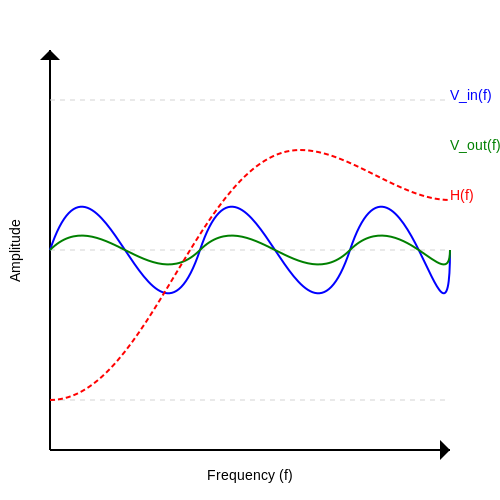
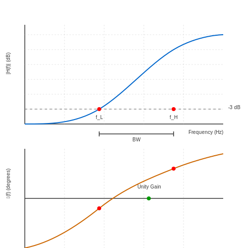
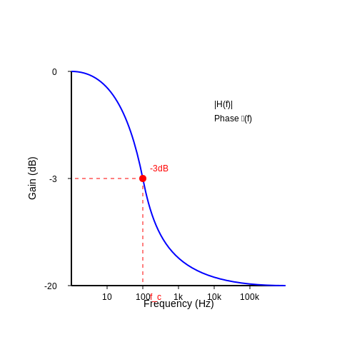
The frequency response of a system characterizes how its output amplitude and phase vary with input frequency. For low-frequency signal conditioning, understanding bandwidth limitations is critical to avoid distortion, aliasing, or signal attenuation. The transfer function H(f) of a linear time-invariant (LTI) system fully describes its frequency response:
where |H(f)| is the magnitude response and ϕ(f) is the phase response. The −3 dB bandwidth defines the frequency range where the signal power remains within half of its peak value.
Bandwidth Limitations in Low-Frequency Systems
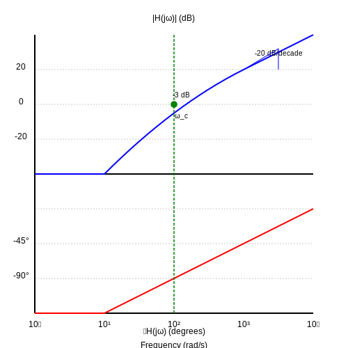
For first-order RC filters, the cutoff frequency f_c is determined by:
Beyond f_c, the signal attenuates at −20 dB/decade. In active filters or amplifiers, the gain-bandwidth product (GBW) imposes a fundamental trade-off:
where A_v is the DC gain. For instrumentation amplifiers, common-mode rejection ratio (CMRR) degrades with frequency, necessitating careful bandwidth selection.
Phase Response and Group Delay
Phase distortion becomes significant when:
is non-constant across the bandwidth. Linear phase response (τ_g = constant) preserves signal integrity, critical in applications like biomedical signal processing or precision sensor readouts.
Practical Implications
- Oversampling: Extends effective bandwidth by reducing aliasing in ADCs.
- Noise Floor: Wider bandwidth increases integrated noise, degrading SNR.
- Stability: Feedback systems require phase margins >45° to avoid oscillations.
2. Operational Amplifiers in Low-Frequency Applications
Operational Amplifiers in Low-Frequency Applications
Ideal Op-Amp Characteristics
An ideal operational amplifier (op-amp) in low-frequency applications exhibits infinite open-loop gain (AOL), infinite input impedance, zero output impedance, and infinite bandwidth. The transfer function of an ideal op-amp in open-loop configuration is:
where V+ and V- are the non-inverting and inverting inputs respectively. In practical low-frequency circuits, negative feedback is applied to make the amplifier characteristics primarily dependent on external components rather than the op-amp's open-loop parameters.
Closed-Loop Configurations
The two fundamental closed-loop configurations are:
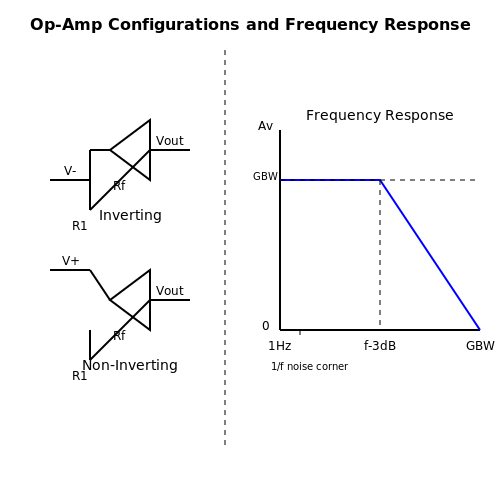
- Inverting amplifier: The input signal is applied to the inverting terminal through an input resistor R1, with feedback resistor Rf determining the gain.
- Non-inverting amplifier: The input signal connects directly to the non-inverting terminal, with feedback applied to the inverting input.
The gain equations for these configurations are derived from the virtual short concept (V+ ≈ V- when in negative feedback):
Frequency Response Considerations
At low frequencies, the dominant pole of an op-amp's internal compensation creates a first-order roll-off. The gain-bandwidth product (GBW) remains constant:
For a closed-loop amplifier with bandwidth fc:
where Av is the closed-loop gain. This relationship demonstrates the fundamental trade-off between gain and bandwidth in op-amp circuits.
Noise Analysis
Low-frequency applications must account for 1/f (flicker) noise, which dominates below the corner frequency (typically 1Hz-1kHz for bipolar op-amps, higher for CMOS). The total input-referred voltage noise density is:
where en,white is the white noise density and en,1/f characterizes the 1/f noise magnitude.
DC Error Sources
Key DC parameters affecting low-frequency performance include:
- Input offset voltage (VOS): Typically 0.1-10mV, causes output DC error of VOS × (1 + Rf/R1)
- Input bias currents (IB+, IB-): Generate voltage drops across source impedances
- CMRR: Rejection of common-mode signals degrades at low frequencies
The total output DC error voltage can be expressed as:
where R2 is the DC resistance seen by the non-inverting input.
Stability in Low-Frequency Circuits
While stability concerns are reduced at low frequencies, several factors remain critical:
- Power supply rejection ratio (PSRR) degradation below 100Hz
- Thermal drift of offset parameters (typically 1-10μV/°C)
- Long-term parameter drift due to aging effects
Proper bypassing (10μF tantalum + 0.1μF ceramic per supply pin) and guard-ring techniques minimize low-frequency disturbances.
Practical Design Example: Low-Noise Preamplifier
A low-noise preamplifier for sensor signals might use:
- JFET-input op-amp for low 1/f noise (e.g., OPA140)
- Gain of 100 (40dB) with Rf = 100kΩ, R1 = 1kΩ
- Input RC filter (fc = 0.16Hz) using 10μF capacitor and 100kΩ resistor
The equivalent input noise voltage in the 0.1-10Hz band would be:
For the OPA140 (en,1/f = 50nV/√Hz at 1Hz, en,white = 5.1nV/√Hz), this yields approximately 150nV rms in the 0.1-10Hz band.
2.2 Gain and Bandwidth Considerations
Fundamental Trade-Offs in Amplifier Design
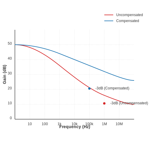
The relationship between gain and bandwidth in low-frequency amplifiers is governed by the gain-bandwidth product (GBW), a fundamental constraint in linear time-invariant systems. For a single-pole amplifier, the GBW remains constant:
where Av is the DC voltage gain and f-3dB is the -3 dB cutoff frequency. This inverse relationship forces designers to make critical trade-offs between amplification and frequency response.
Multi-Stage Amplifier Analysis
When cascading multiple amplifier stages, the overall bandwidth reduction follows the nth-order pole interaction. For n identical stages with individual bandwidth f1:
This results in a 64% bandwidth reduction for two stages and 51% for three stages compared to a single-stage implementation. The total gain multiplies while the system bandwidth contracts.
Slew Rate Limitations
At low frequencies, slew rate (SR) becomes the dominant limitation for large-signal bandwidth:
where fmax is the maximum full-power frequency before distortion occurs. For a typical operational amplifier with SR = 0.5 V/μs driving a 10 V peak signal, the full-power bandwidth is just 8 kHz.
Noise-Gain Effects
The effective bandwidth is further modified by the noise gain (Gn) in non-inverting configurations:
This explains why unity-gain stable amplifiers maintain better bandwidth characteristics compared to decompensated designs when configured for low closed-loop gains.
Practical Compensation Techniques
- Dominant pole compensation: Introduces a low-frequency pole to stabilize the amplifier while maintaining phase margin
- Miller compensation: Uses capacitor multiplication to effectively shift the dominant pole without requiring large physical capacitors
- Feedforward techniques: Bypass high-frequency signals around slow stages to preserve bandwidth
Thermal Considerations in High-Gain Designs
Power dissipation in high-gain stages follows:
where β is the feedback factor. This quadratic relationship with gain necessitates careful thermal management in precision low-frequency amplifiers, particularly when driving low-impedance loads.
2.3 Noise Reduction in Amplifier Circuits
Noise in amplifier circuits arises from both intrinsic and extrinsic sources, including thermal noise, shot noise, flicker noise, and electromagnetic interference. Minimizing noise is critical in low-frequency applications where signal integrity is paramount. The following strategies address noise reduction systematically.
Thermal Noise Mitigation
Thermal noise, or Johnson-Nyquist noise, is inherent in resistive components and follows:
where kB is Boltzmann’s constant, T is temperature in Kelvin, R is resistance, and Δf is bandwidth. To reduce thermal noise:
- Minimize resistive components in signal paths.
- Use low-noise materials (e.g., metal-film resistors).
- Operate at lower temperatures where feasible.
Low-Noise Amplifier (LNA) Design
The noise figure (NF) quantifies degradation in signal-to-noise ratio (SNR):
Optimal LNA design involves:
- Selecting transistors with low noise parameters (e.g., JFETs or SiGe HBTs).
- Impedance matching to minimize reflections.
- Biasing devices in their optimal noise regions.
Grounding and Shielding Techniques
Electromagnetic interference (EMI) couples into circuits via conductive, capacitive, or inductive paths. Countermeasures include:
- Star grounding: Single-point grounding avoids ground loops.
- Shielded enclosures: Faraday cages block external fields.
- Twisted-pair wiring: Reduces magnetic field coupling.
Filtering Strategies
Bandwidth-limiting filters suppress out-of-band noise. For a first-order RC filter:
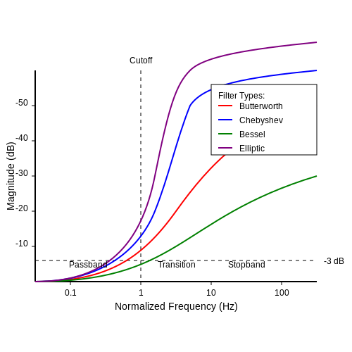
Higher-order filters (Butterworth, Bessel) provide steeper roll-off but introduce phase distortion. Active filters with operational amplifiers allow tunable cutoff frequencies without passive component limitations.
Differential Signaling
Differential amplifiers reject common-mode noise by amplifying only the voltage difference between inputs. The common-mode rejection ratio (CMRR) is:
where Ad is differential gain and Acm is common-mode gain. High CMRR (>100 dB) is achievable with precision-matched resistors and instrumentation amplifiers.
Practical Case: EEG Signal Amplification
In electroencephalography (EEG), signals range from 0.5–100 µV with strong 50/60 Hz interference. A typical solution combines:
- Differential amplification (CMRR > 120 dB).
- Notch filtering at line frequency.
- Shielded cables with driven-right-leg (DRL) circuits to cancel body-coupled noise.
3. Passive vs. Active Filters for Low Frequencies
3.1 Passive vs. Active Filters for Low Frequencies
Fundamental Differences
Passive filters consist solely of passive components—resistors (R), capacitors (C), and inductors (L)—without any external power source. The transfer function of a first-order passive RC low-pass filter is given by:
where s is the complex frequency variable. The cutoff frequency (fc) occurs at:
Active filters incorporate operational amplifiers (op-amps) or transistors, enabling signal amplification and higher input impedance. A basic first-order active low-pass filter with gain K has the transfer function:
Performance Tradeoffs at Low Frequencies
For sub-100Hz applications, passive filters face critical limitations:
- Component size: Achieving low fc requires impractically large capacitors (e.g., 160μF for 10Hz with 100Ω).
- Load sensitivity: Impedance mismatches alter filter characteristics, as the output impedance is not buffered.
- Signal attenuation: Passive networks cannot compensate for insertion loss.
Active filters overcome these issues through:
- Size reduction: Op-amp feedback networks enable smaller capacitors (nF range) for the same cutoff frequency.
- Impedance isolation: High input and low output impedance prevent loading effects.
- Gain integration: Simultaneous amplification and filtering reduces stage count.
Noise and Dynamic Range Considerations
Active filters introduce op-amp noise (en) and current noise (in), which dominate at low frequencies due to the 1/f noise characteristic. The total output noise voltage in a non-inverting active filter is:
where k is Boltzmann's constant and T is absolute temperature. Passive filters avoid active noise sources but may require subsequent amplification, potentially degrading the signal-to-noise ratio.
Practical Implementation Challenges
DC offset becomes significant in active filters below 10Hz. The input offset voltage (VOS) of the op-amp appears at the output multiplied by the DC gain:
This necessitates:
- Chopper-stabilized op-amps for sub-Hz applications
- Precision resistor networks (0.1% tolerance or better)
- Polypropylene or polystyrene capacitors for stable temperature performance
Case Study: Seismic Sensor Conditioning
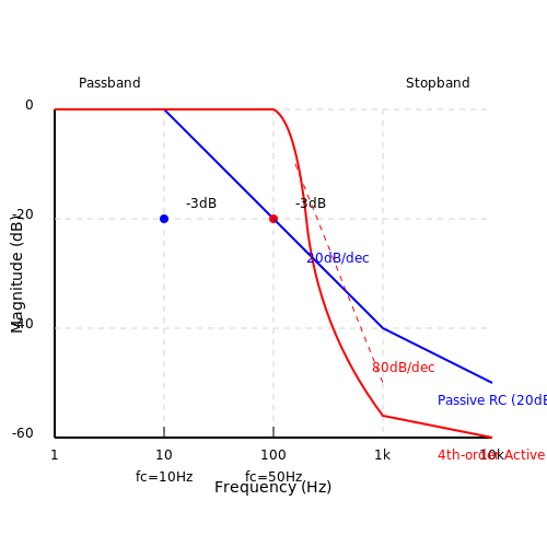
In a 0.1-50Hz geophone amplifier, a 4th-order Butterworth response was implemented using:
- Passive stage: Initial 100Hz anti-alias RC filter (R=10kΩ, C=160nF)
- Active stages: Two Sallen-Key sections with fc=50Hz using OPA2188 op-amps
- Result: 0.1dB passband ripple, 80dB/decade rolloff, and 1.5μV/√Hz input-referred noise
3.2 Designing High-Pass and Low-Pass Filters
Fundamentals of Passive RC Filters
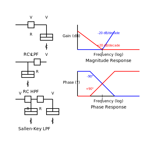
The simplest form of high-pass (HPF) and low-pass (LPF) filters consists of a resistor (R) and capacitor (C) in series. The cutoff frequency (fc) for both filters is determined by:
For an LPF, the capacitor is placed in parallel with the output, attenuating frequencies above fc. Conversely, an HPF places the resistor in parallel with the output, attenuating frequencies below fc.
Transfer Functions and Bode Plots
The transfer function H(s) of a first-order LPF is:
For an HPF, the transfer function becomes:
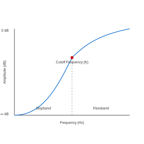
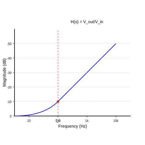
Bode plots for these filters show a roll-off of 20 dB/decade beyond the cutoff frequency. The phase shift transitions from 0° to −90° (LPF) or +90° to 0° (HPF) centered at fc.
Active Filter Design
Passive RC filters suffer from loading effects and lack gain. Active filters, using operational amplifiers (op-amps), overcome these limitations. A Sallen-Key topology is commonly used for second-order filters, improving roll-off to 40 dB/decade.
The transfer function for a second-order LPF in Sallen-Key configuration is:
where K is the gain (set by feedback resistors). For an HPF, capacitors and resistors swap positions.
Component Selection and Practical Considerations
Key design parameters include:
- Cutoff frequency accuracy – Depends on component tolerances (use 1% resistors and NP0/C0G capacitors).
- Op-amp bandwidth – Must exceed the filter's intended frequency range.
- Q factor – Determines peaking near fc; for Butterworth filters, Q = 0.707 ensures maximally flat response.
For example, a Butterworth LPF with fc = 1 kHz and Q = 0.707 requires:
Real-World Applications
High-pass filters are used in:
- AC coupling to block DC offsets.
- Audio systems to remove rumble noise below 20 Hz.
Low-pass filters are applied in:
- Anti-aliasing before analog-to-digital conversion.
- Noise reduction in sensor signal chains.
3.3 Notch Filters for Specific Frequency Rejection
Notch filters, also known as band-stop filters, are designed to attenuate a narrow frequency band while allowing signals outside this band to pass with minimal distortion. These filters are particularly useful in applications where interference from a specific frequency (e.g., power-line noise at 50/60 Hz) must be suppressed without affecting the rest of the signal spectrum.
Transfer Function and Frequency Response
The second-order notch filter transfer function is given by:
where:
- \(\omega_0\) is the center frequency (rad/s) of the notch,
- \(Q\) is the quality factor, determining the filter's bandwidth.
The magnitude response of the filter exhibits a sharp null at \(\omega_0\), with the depth of the notch and its bandwidth controlled by \(Q\). Higher \(Q\) values result in a narrower stopband.
Active Twin-T Notch Filter
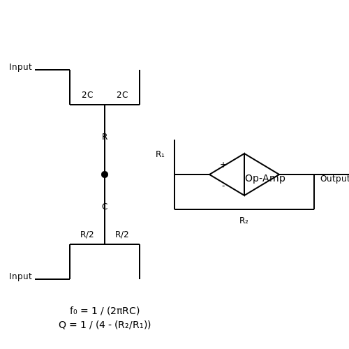
A common implementation is the active Twin-T notch filter, which combines passive RC networks with an op-amp for improved performance. The Twin-T network consists of two T-shaped RC circuits—one high-pass and one low-pass—connected in parallel. The null frequency is determined by:
The op-amp provides gain and compensates for passive component tolerances, ensuring a deep and precise notch. The feedback path adjusts the \(Q\) factor, allowing tunability.
Design Considerations
Key parameters in notch filter design include:
- Notch Depth: The attenuation at \(\omega_0\), ideally infinite but limited by component non-idealities.
- Bandwidth: Defined as \(\text{BW} = \frac{\omega_0}{Q}\), must be narrow enough to reject the target frequency without affecting adjacent signals.
- Component Sensitivity: Passive component tolerances can shift \(f_0\) or degrade notch depth; precision resistors and capacitors are recommended.
Practical Applications
Notch filters are widely used in:
- Biomedical Instrumentation: Removing 50/60 Hz power-line interference from ECG or EEG signals.
- Audio Processing: Eliminating hum or feedback tones in recording equipment.
- Communications: Suppressing carrier frequencies or jamming signals in RF systems.
Step-by-Step Design Example
To design a 60 Hz notch filter with \(Q = 5\):
- Choose \(R = 26.5 \text{k}\Omega\) and \(C = 0.1 \mu\text{F}\) for \(f_0 = 60 \text{Hz}\).
- Calculate the feedback resistor ratio to set \(Q\) in an active Twin-T configuration.
- Simulate the circuit in SPICE to verify notch depth and bandwidth.
where \(R_1\) and \(R_2\) are feedback network resistors.
4. Sampling Rate and Aliasing Issues
4.1 Sampling Rate and Aliasing Issues
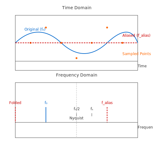
The Nyquist-Shannon sampling theorem states that a continuous signal must be sampled at a rate fs greater than twice its highest frequency component fmax to avoid aliasing. Mathematically, this is expressed as:
When this condition is violated, higher-frequency components fold back into the Nyquist bandwidth, creating false low-frequency artifacts. This phenomenon is particularly problematic in low-frequency signal conditioning, where signals of interest often reside close to DC.
Mathematical Derivation of Aliasing
Consider a sinusoidal signal x(t) = A sin(2πf0t) sampled at intervals Ts = 1/fs. The sampled sequence becomes:
If f0 > fs/2, we can define an alias frequency falias = |f0 - kfs| where k is an integer that brings falias into the Nyquist range [0, fs/2]. This creates an indistinguishable replica of the original signal:
Practical Implications in Low-Frequency Systems
In low-frequency applications (DC-1kHz), several challenges emerge:
- Anti-aliasing filter design requires extremely sharp roll-off near fs/2 while maintaining phase linearity
- 1/f noise can alias into the measurement bandwidth when sampled improperly
- Long settling times of high-order analog filters may distort transient responses
Oversampling Techniques
Modern delta-sigma ADCs employ oversampling ratios (OSR) of 64× to 256× to:
- Relax anti-aliasing filter requirements
- Spread quantization noise over a wider bandwidth
- Enable digital filtering in post-processing
The effective resolution enhancement in bits is given by:
Case Study: Seismic Sensor Array
A 24-bit seismic acquisition system sampling at 500Hz must contend with:
- Microseismic signals as low as 0.01Hz
- Cultural noise peaks at 60Hz and harmonics
- Anti-aliasing filter cutoff at 200Hz with >120dB/octave rejection
The system employs a 5th-order switched-capacitor filter followed by a 128× oversampled delta-sigma modulator, achieving 18.5 effective bits of resolution in the 0.1-50Hz band of interest.
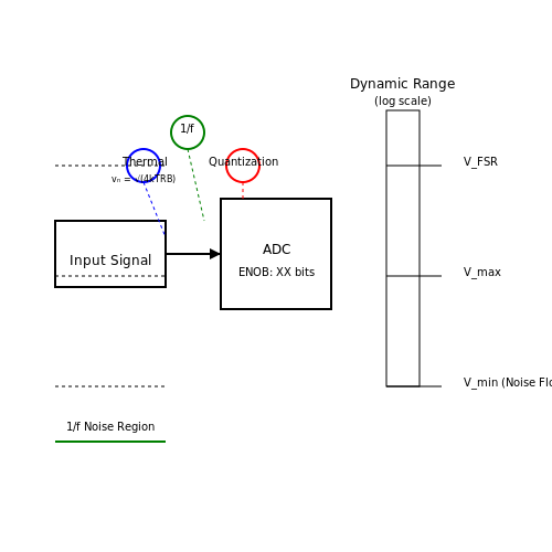
4.2 Resolution and Dynamic Range Considerations
Fundamental Definitions
The resolution of a signal conditioning system refers to the smallest detectable change in the input signal, typically quantified in bits for digital systems or microvolts for analog systems. For an N-bit analog-to-digital converter (ADC), the theoretical resolution is given by:
where VFSR is the full-scale range of the ADC. In low-frequency applications, thermal noise and 1/f noise often dominate, imposing practical limits below this theoretical value.
Dynamic Range and Noise Floor
The dynamic range (DR) is the ratio between the largest and smallest signals a system can process simultaneously, expressed in decibels:
The lower bound Vmin is determined by the noise floor, which integrates contributions from Johnson-Nyquist noise, amplifier noise, and quantization noise. For a bandwidth B, the thermal noise voltage in a resistor R is:
where k is Boltzmann's constant and T is the absolute temperature. This noise sets a fundamental limit on achievable resolution.
Trade-offs in Low-Frequency Systems
In DC and near-DC applications, 1/f noise becomes significant, scaling inversely with frequency. Chopper stabilization and auto-zeroing techniques are often employed to mitigate this. The effective number of bits (ENOB) for a system with signal-to-noise-and-distortion ratio (SINAD) is:
Practical implementations must balance filter cutoff frequencies (to reduce noise bandwidth) against time-domain settling requirements. For example, a 24-bit delta-sigma ADC may achieve 20-bit ENOB at 10 Hz but only 16-bit at 0.1 Hz due to 1/f noise dominance.
Case Study: Seismic Sensor Interface
A high-resolution seismometer system with 5 nV/√Hz input noise requires:
- Sub-microvolt offset cancellation (e.g., correlated double sampling)
- Multi-pole anti-aliasing filtering below 0.01 Hz
- 24-bit ADC with programmable gain to handle ±2 V signals while resolving 100 nV steps
The achieved dynamic range exceeds 140 dB, but only when accounting for 104-second averaging to suppress 1/f noise below 0.1 Hz.
Quantization Error Analysis
The RMS quantization error for an ideal ADC is:
In oversampled systems, this error spreads across Nyquist bandwidth, allowing noise shaping. For oversampling ratio OSR, the quantization noise power decreases as:
where L is the modulator order. This principle enables delta-sigma converters to achieve 24+ bit resolution in narrow bandwidths.
4.3 Anti-Aliasing Filter Design
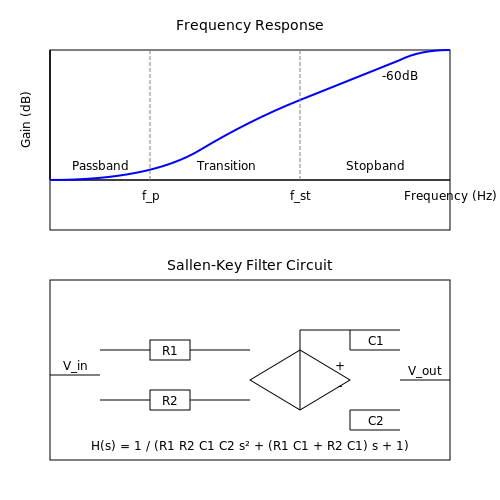
Anti-aliasing filters are critical in sampled-data systems to prevent higher-frequency components from folding back into the desired signal bandwidth. The filter must attenuate frequencies above the Nyquist frequency (fs/2) to a level below the quantization noise floor of the analog-to-digital converter (ADC).
Filter Specifications
The design begins with defining the passband (fp), stopband (fst), passband ripple (Ap), and stopband attenuation (Ast). For a sampling rate fs, the Nyquist criterion requires:
The transition ratio (k) determines the filter order:
Butterworth Filter Design
Butterworth filters provide maximally flat passband response. The minimum order N is calculated from:
The cutoff frequency fc for a normalized Butterworth filter scales as:
Active Filter Implementation
Sallen-Key and multiple-feedback topologies are common for low-frequency anti-aliasing. For a 2nd-order Sallen-Key low-pass filter:
where Q is the quality factor and ω0 is the cutoff frequency in radians/second. Component values for unity gain are:
Practical Considerations
- Phase linearity: Bessel filters preserve waveform shape at the cost of slower roll-off
- Op-amp selection: Choose amplifiers with gain-bandwidth product ≥ 100×fc
- Component tolerance: 1% resistors and C0G/NP0 capacitors minimize cutoff frequency drift
Frequency-Domain Verification
Measure the filter's transfer function using a network analyzer. Key metrics:
5. Biomedical Signal Conditioning
5.1 Biomedical Signal Conditioning
Biomedical signals, such as electrocardiograms (ECG), electroencephalograms (EEG), and electromyograms (EMG), typically operate in the microvolt to millivolt range with frequencies spanning 0.01 Hz to 10 kHz. Effective conditioning of these signals requires precise amplification, filtering, and isolation to extract diagnostically relevant information while rejecting noise and interference.
Noise Sources in Biomedical Signals
Biological signals are contaminated by multiple noise sources:
- Powerline interference (50/60 Hz) – Coupled capacitively or inductively into measurement leads.
- Electrode contact noise – Caused by impedance variations due to skin movement or poor contact.
- Motion artifacts – Low-frequency disturbances from patient movement.
- Baseline wander – Slow DC shifts due to respiration or perspiration.
- Electromagnetic interference (EMI) – Radiated noise from nearby electronic devices.
Instrumentation Amplifier Design
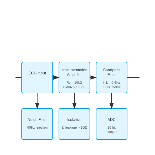
The first stage of biomedical signal conditioning typically employs an instrumentation amplifier (IA) to achieve high common-mode rejection ratio (CMRR) and differential gain. The transfer function of a 3-op-amp IA is derived as follows:
Where Rg sets the gain, while R1, R2, and R3 must be matched to maintain high CMRR (>100 dB). Modern integrated IAs (e.g., AD620, INA128) achieve 0.1% gain accuracy with 90 dB CMRR at 60 Hz.
Active Filtering Techniques
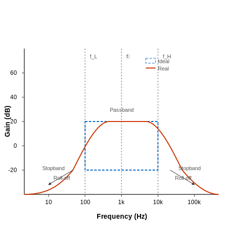
Biomedical signals require bandpass filtering to eliminate out-of-band noise. A second-order Sallen-Key bandpass filter with cutoff frequencies fL and fH can be implemented using:
For ECG signals (0.05–150 Hz), a 60 Hz notch filter is often added using a twin-T network with quality factor Q:
where K is the gain at the notch frequency.
Isolation and Patient Safety
Galvanic isolation using optocouplers or isolation amplifiers (e.g., ISO124) is critical to prevent leakage currents exceeding 10 μA (IEC 60601-1 standard). A transformer-coupled isolation stage provides:
where Zleakage must exceed 1 MΩ at 50 Hz to meet medical safety standards.
Case Study: ECG Front-End Design
A typical ECG conditioning chain includes:
- Right-leg drive (RLD) circuit to reduce common-mode voltage.
- 0.05 Hz high-pass filter to eliminate baseline wander.
- 150 Hz low-pass anti-aliasing filter.
- 12-bit ADC with at least 500 SPS sampling rate.
Modern implementations use fully integrated solutions like the ADS1298, which combines 8 channels with programmable gain and digital filtering.
5.2 Industrial Sensor Signal Processing
Noise Mitigation in Low-Frequency Sensor Signals
Low-frequency industrial sensors (e.g., strain gauges, thermocouples) are susceptible to 1/f noise and electromagnetic interference (EMI). The signal-to-noise ratio (SNR) degradation follows:Active Filtering and Amplification
A 2-stage active filter (Sallen-Key topology) is often employed. The transfer function for a 2nd-order low-pass filter is:Analog-to-Digital Conversion Strategies
Delta-sigma ADCs outperform successive-approximation (SAR) ADCs for frequencies below 1 kHz due to oversampling and noise shaping. The effective number of bits (ENOB) is:Practical Implementation: RTD Signal Chain
For a Pt100 RTD (Resistance Temperature Detector), a 3-wire configuration cancels lead resistance errors. The current source \( I_{\text{excite}} \) and reference resistor \( R_{\text{ref}} \) set the gain:Case Study: Vibration Sensor Conditioning
A piezoelectric accelerometer’s charge output (\( Q = d_{33}F \)) requires a charge amplifier with feedback capacitance \( C_f \):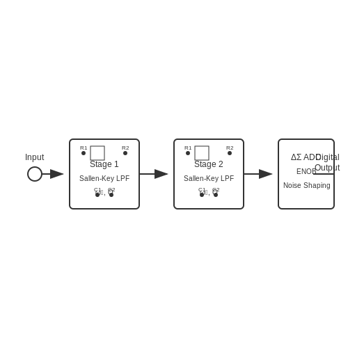
5.3 Audio Signal Conditioning
Fundamentals of Audio Signal Processing
Audio signals typically occupy the frequency range of 20 Hz to 20 kHz, with human speech concentrated between 300 Hz and 3.4 kHz. Conditioning these signals involves amplification, filtering, impedance matching, and noise suppression to ensure fidelity and compatibility with downstream processing stages. The primary challenge lies in maintaining signal integrity while minimizing harmonic distortion and intermodulation effects.
Amplification and Gain Control
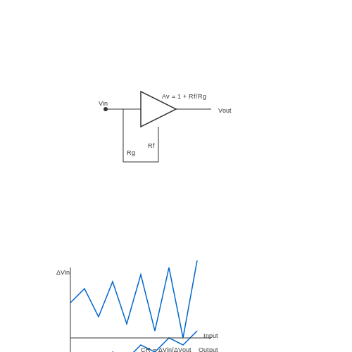
Low-noise amplification is critical in audio signal chains. The signal-to-noise ratio (SNR) must be preserved, particularly for weak signals from microphones or sensors. A non-inverting operational amplifier configuration is often employed for its high input impedance and low output impedance:
where Av is the voltage gain, Rf is the feedback resistor, and Rg is the ground resistor. Automatic gain control (AGC) circuits dynamically adjust gain to prevent clipping while maintaining adequate signal levels.
Filtering and Equalization
Bandpass filtering removes out-of-band noise, while notch filters suppress specific interference frequencies (e.g., 50/60 Hz power-line hum). A second-order Sallen-Key filter provides a balance between roll-off steepness and phase linearity:
where ω0 is the center frequency and Q is the quality factor. Graphic equalizers use multiple bandpass filters to shape frequency response, while parametric equalizers allow precise adjustment of center frequency, bandwidth, and gain.
Dynamic Range Compression
Compressors reduce the dynamic range of audio signals by attenuating peaks, ensuring consistent levels for transmission or recording. The compression ratio CR defines the input-to-output level relationship:
A ratio of 4:1 indicates that a 4 dB increase in input level yields only a 1 dB increase in output. Threshold and attack/release time constants must be carefully tuned to avoid audible artifacts.
Impedance Matching and Buffering
Mismatched impedances cause signal reflections and power loss. For instance, microphone preamps typically require input impedances ≥1 kΩ to avoid loading high-impedance condenser microphones. Unity-gain buffers using op-amps (e.g., voltage followers) isolate stages while maintaining signal integrity.
Noise Reduction Techniques
Common-mode rejection in differential amplifiers suppresses interference, while shielding and twisted-pair wiring minimize electromagnetic pickup. Digital signal processing (DSP) techniques, such as adaptive filtering and spectral subtraction, further enhance SNR in post-processing.
Practical Implementation Considerations
Component selection significantly impacts performance. Low-tolerance resistors (±1%) and polypropylene capacitors ensure stable filter characteristics, while low-noise op-amps (e.g., NE5532, OPA1612) minimize thermal and flicker noise. PCB layout must minimize parasitic capacitance and ground loops to preserve high-frequency response.
6. Recommended Textbooks and Papers
6.1 Recommended Textbooks and Papers
- SIGNAL ANALYSIS - Wiley Online Library — 6.5.1 Frequency Translation and Amplitude Modulation 469 6.5.2 Baseband Signal Recovery 470 6.5.3 Angle Modulation 471 6.6 Summary 475 References 476 Problems 477 7 Discrete Fourier Transforms 482 7.1 Discrete Fourier Transform 483 7.1.1 Introduction 484 7.1.2 The DFT's Analog Frequency-Domain Roots 495 7.1.3 Properties 497
- PDF SENSORS AND SIGNAL CONDITIONING - Wiley — 5.2.5 ac/dc signal converters, 294 5.3 Carrier Amplifiers and Coherent Detection, 299 5.3.1 Fundamentals and structure of carrier amplifiers, 299 5.3.2 Phase-sensitive detectors, 306 5.3.3 Application to LVDTs, 311 5.4 Specific Signal Conditioners for Capacitive Sensors, 313 5.5 Resolver-to-Digital and Digital-to-Resolver Converters, 316
- (PDF) Signal Conditioning - Academia.edu — The entire content is intentionally segregated in two parts namely ''Continuous wave communication and analog signal conditioning'' and ''Discrete signal conditioning: 1D and 2D''. The 1st part comprises of the continuous time Fourier series and transform, and the basic analog modulations like amplitude, frequency and phase ...
- Instrumentation, Signal Conditioning, and Filters - SPIE Digital Library — Several chapters back, we began with the basic components used in electronics and then moved to exploring analog and digital electronics, and processing electrical signals. We can now begin to convert this understanding of basic electronics into an ability to design and plan more complicated instruments. Even the most complicated instruments are made up of simpler instruments and electronic ...
- PDF Instrumentation & Measurements MECH 430 Chapter 6 Signal Conditioning — The raw signal generated by most passive sensors may be in the order of mV or nA. A thermocouple with one iron arm (high emf at +3.54mV) and one nickel arm (low emf at - 3.1mV) produces an output of 6.64 mV for ∆T =200oC. A photodiode has a current output of 10μA when illuminated and 10nA in total darkness. Typical signal range of common ...
- PDF Lecture 4: Signal Conditioning - MECHATRONICS ENGINEERING DEPARTMENT — Typical Roles of Signal Conditioning • Signal Conditioning - Provides external excitation and grounding - Completes the circuit (bridges) - Linearizes - Filters (typically low pass filter which only allows low frequency signals through) - Amplifies - Isolates one part of a system electrically from other parts of the system - Typical input is in millivolts, output is in volts
- PDF General Signal Conditioning Guide - PCB — 7.1.1 Effect of DTC on Low Frequency Response..... 16 7.1.2 Effect of DTC on Long Duration Time ... external signal conditioner before analyzing any data. This concept will be fully explained later.) Also, the impedance level at the . output of the sensor is less than 100 ohms. This makes it easy to drive long cables through harsh environments ...
- Signal Conditioning - Springer — SIGNAL CONDITIONING 279 6.1.2 Capacitive Divider The voltage dividers so far described have been mainly applicable for d.c. and low frequency a.c. The capacitive divider is basically unsuitable for d.c. use, since voltage division would then rely on leakage current, but it may be used on a.c. from power frequencies to MHz.
- Electronics for Technicians - 1st Edition - Elsevier Shop — 5.3.3. Use of Small-Signal Equivalent Circuits to Determine the Voltage Gain of a Simple Amplifier 5.3.4. Input Resistance, Output Resistance and Matching 5.3.5. R.C.-Coupled Thermionic Valve Amplifier 5.3.6. Transformer-Coupled and Tuned-Anode Voltage Amplifiers 5.3.7. Resistance-Loaded Large-Signal Valve Amplifiers 5.4.
- Interface Electronic Circuits - SpringerLink — The front end of a signal conditioner depends on type of the sensor's output electrical characteristics. Table 6.1 lists five basic types of the sensor output properties: voltage, current, resistive, capacitive, and inductive. Selecting the appropriate input stage of a signal conditioner is essential for the optimal data collection.
6.2 Online Resources and Tutorials
- PDF Signal Acquisition and Conditioning With Low Supply Voltages — This signal is applied to the input of a differential amplifier that consists of the TLV2262 operational amplifier and the resistance network that sets the amplification. Capacitor C1 acts as a low-pass filter to suppress high-frequency interference . _ + TLV1543 Digital Interface R1 R2 R3 C1 VCC VCC VO VCC V1 V2 ROT R + ∆R R - ∆R R ...
- (PDF) Signal Conditioning - Academia.edu — The generic chapter on preview and introduction starts with discussing about the fundamental properties and operations in signals and systems. The entire content is intentionally segregated in two parts namely ''Continuous wave communication and analog signal conditioning'' and ''Discrete signal conditioning: 1D and 2D''.
- PDF General Signal Conditioning Guide - PCB — 6. 2.2 CHARGE AMPLIFIED SYSTEMS. A typical charge amplified measurement system is shown . below in Figure 3. A schematic representation of a charge amplified system, including sensor, cable and charge amplifier, is shown in . Figure 4. Once again, the insulation resistance (resistance between signal and ground) is assumed to be large (>1012
- Active Low Pass Filter - Op-amp Low Pass Filter — Gain of a first-order low pass filter. Where: A F = the pass band gain of the filter, (1 + R2/R1); ƒ = the frequency of the input signal in Hertz, (Hz); ƒc = the cut-off frequency in Hertz, (Hz); Thus, the operation of a low pass active filter can be verified from the frequency gain equation above as:
- PDF Fundamentals of Electronic Circuit Design - University of Cambridge — 1.5 Electronic Signals Electronic signals are represented either by voltage or current. The time-dependent characteristics of voltage or current signals can take a number of forms including DC, sinusoidal (also known as AC), square wave, linear ramps, and pulse-width modulated signals. Sinusoidal signals are perhaps the most important signal forms
- PDF Ch6. Small Signal Analysis of LLC Resonant Converter - Virginia Tech — converter, the natural frequency of the linear network (output filter) is much lower than the switching frequency. The modulation of the converter is achieved through the low frequency content in the control signal. With this character, the average method can provide approximate linear solution of the nonlinear state equations.
- Passive Low Pass Filter - Passive RC Filter Tutorial — The Bode Plot shows the Frequency Response of the filter to be nearly flat for low frequencies and all of the input signal is passed directly to the output, resulting in a gain of nearly 1, called unity, until it reaches its Cut-off Frequency point ( ƒc). This is because the reactance of the capacitor is high at low frequencies and blocks any ...
- PDF General Signal Conditioning Guide - PCB — SIGNAL CONDITIONING GUIDE5 bias level is constant and results from the electrical proper-ties of the amplifier itself. (Normally, the bias level is removed by an external signal conditioner before analyzing any data. This concept will be fully explained later.) Also, the imped-ance level at the output of the sensor is less than 100 ohms.
- 6.02 Tutorial 1 | Introduction to EECS II: Digital Communication ... — This resource contains information regarding tutorial 1. Browse Course Material Syllabus ... Signal Processing; Telecommunications; Learning Resource Types assignment Problem Sets. grading Exams. ... This resource contains information regarding tutorial 1. Resource Type: Tutorials. pdf.
- Introduction to EECS II: Digital Communication Systems | Electrical ... — An introduction to several fundamental ideas in electrical engineering and computer science, using digital communication systems as the vehicle. The three parts of the course—bits, signals, and packets—cover three corresponding layers of abstraction that form the basis of communication systems like the Internet. The course teaches ideas that are useful in other parts of EECS: abstraction ...
6.3 Advanced Topics for Further Study
- Readings | Introductory Analog Electronics Laboratory | Electrical ... — Further reading on a wide variety of analog electronics topics is suggested in this list of references, compiled by the course staff. Readings by Session ... C. Common-emitter large signal model, graphical analysis Neamen 5.2 to 5.2.3 and 5.3.3, J&J pp. 216-220, Cathey 3.6 to 3.7 ... D. Low frequency incremental model Neamen 4.9 to 4.9.2 E ...
- PDF Instrumentation & Measurements MECH 430 Chapter 6 Signal Conditioning — The raw signal generated by most passive sensors may be in the order of mV or nA. A thermocouple with one iron arm (high emf at +3.54mV) and one nickel arm (low emf at - 3.1mV) produces an output of 6.64 mV for ∆T =200oC. A photodiode has a current output of 10μA when illuminated and 10nA in total darkness. Typical signal range of common ...
- PDF SECTION 3 HIGH RESOLUTION SIGNAL CONDITIONING ADCs - Analog — LOW POWER, LOW VOLTAGE ADC DESIGN ISSUES Low Power ADCs typically run on 5V, +5V, +5/+3V, or +3V Lower Signal Swings Increase Sensitivity to All Types of Noise (Device, Power Supply, Logic, etc.) Device Noise Increases at Low Quiescent Currents Bandwidth Suffers as Supply Current Drops Input Common-Mode Range May be Limited
- PDF Signal Acquisition and Conditioning With Low Supply Voltages — 3-V Supply Signal Processing Limitations 2 SLAA018 2 3-V Supply Signal Processing Limitations Many electronic systems use a 5-V supply because of the widespread use of the SN74 family of logic devices. The demand for improvements in the characteristics and performance of portable electronic equipment, however, led to new families
- Interface electronics and conditioning circuits for triboelectric ... — This chapter provides an overview of signal-conditioning circuits for triboelectric-based sensors along with several design examples. A signal-conditioning circuit that can process the real-time signal generated by a triboelectric-based, grating-structured control interface is presented in a case study.
- PDF Section 4 Sensor to ADC Design Wireless Communication - Texas Instruments — Texas Instruments 4 -1 Signal Conditioning Seminar Texas Instruments Signal Conditioning Seminar 4 -1 Section 4 Sensor to ADC Design Wireless Communication Signal Conditioning for IF Sampling High -speed op amps are used extensively in wireless communications. These amplifiers usually operate below 500MHz, and often they operate at 25MHz and below.
- PDF Chapter 6 SIGNAL PROCESSING FOR IMPROVED DETECTIVITY - TU Delft OCW — Electronic Instrumentation R.F. Wolffenbuttel Chapter 6: SIGNAL PROCESSING FOR IMPROVED DETECTIVITY 150 If noise is the dominating source of uncertainty, then the detection limit is the signal power that is determined by the noise spectral power of the equivalent input noise sources over the measurement bandwidth, with the specified SNR.
- PDF General Signal Conditioning Guide - PCB — Low per-channel cost as sensors require only low-cost, constant current signal conditioners and ordinary cables. 7 . Reduced system maintenance. 8 . Direct operation into readout and data acquisition instruments, which incorporate power for use with . PCB's ICP ® sensors. Figure 6 schematically shows the electrical fundamentals of
- (PDF) Signal Conditioning - Academia.edu — The generic chapter on preview and introduction starts with discussing about the fundamental properties and operations in signals and systems. The entire content is intentionally segregated in two parts namely ''Continuous wave communication and analog signal conditioning'' and ''Discrete signal conditioning: 1D and 2D''.