Leakage Current in Semiconductors
1. Definition and Basic Concepts of Leakage Current
Definition and Basic Concepts of Leakage Current
Leakage current in semiconductors refers to the unintended flow of electric charge across a device or junction when it is nominally in the off-state. Unlike the desired conduction current, leakage arises due to quantum mechanical effects, thermal excitation, or defects in the material structure. In modern nanoscale devices, leakage currents can dominate power dissipation and degrade performance.
Physical Origins of Leakage Current
Leakage current manifests through several mechanisms:
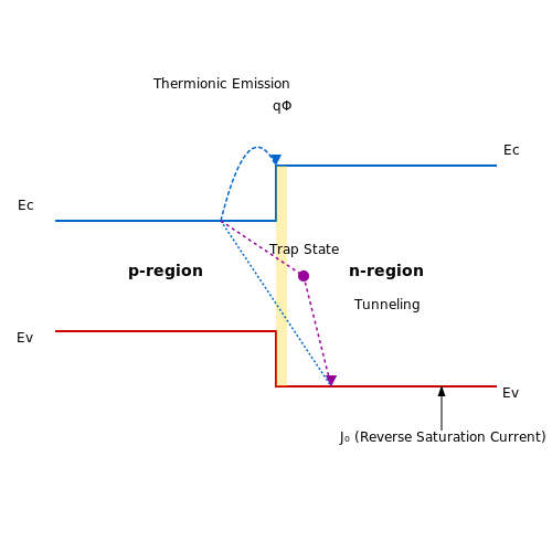
- Thermionic emission – Charge carriers overcome the potential barrier due to thermal energy.
- Tunneling – Quantum mechanical tunneling through thin potential barriers (direct or Fowler-Nordheim).
- Diffusion current – Minority carriers diffuse across junctions even under reverse bias.
- Defect-assisted conduction – Trap states or dislocations provide alternative conduction paths.
In MOSFETs, subthreshold leakage occurs when the gate voltage is below the threshold but carriers still traverse the channel via thermal injection. Gate oxide tunneling becomes significant when oxide thickness scales below 2 nm.
Mathematical Modeling
The reverse saturation current density in a p-n junction is given by:
where q is the electron charge, D represents diffusion coefficients, L diffusion lengths, and pn, np minority carrier concentrations.
For subthreshold leakage in MOSFETs, the current follows:
where VT is the thermal voltage (≈26 mV at 300K), n the ideality factor, and Vth the threshold voltage.
Practical Implications
In integrated circuits, leakage currents:
- Increase static power consumption (Pleak = VDD × Ileak).
- Cause signal integrity issues in dynamic logic.
- Limit transistor scaling due to exponential rise in tunneling currents.
Advanced techniques like high-κ dielectrics, strained silicon, and FinFET architectures aim to mitigate leakage while maintaining performance.
1.2 Role of Charge Carriers in Leakage Current
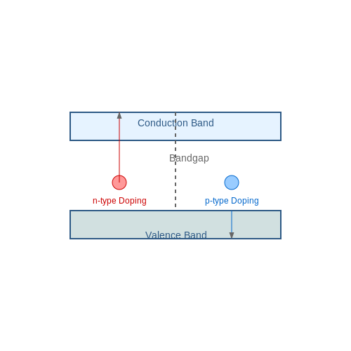
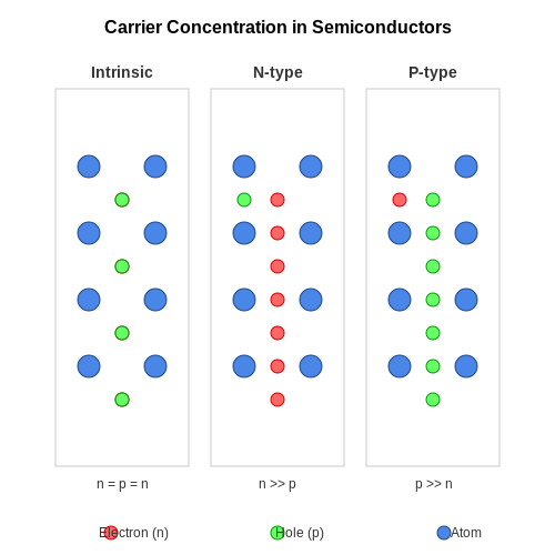
Leakage current in semiconductors arises primarily from the movement of charge carriers across potential barriers or through defect states when no external bias is applied. The two dominant charge carriers—electrons in the conduction band and holes in the valence band—contribute to leakage via distinct mechanisms governed by their respective energy states and mobility.
Thermally Generated Carriers
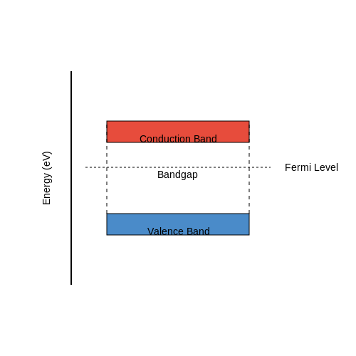
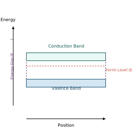
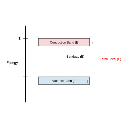
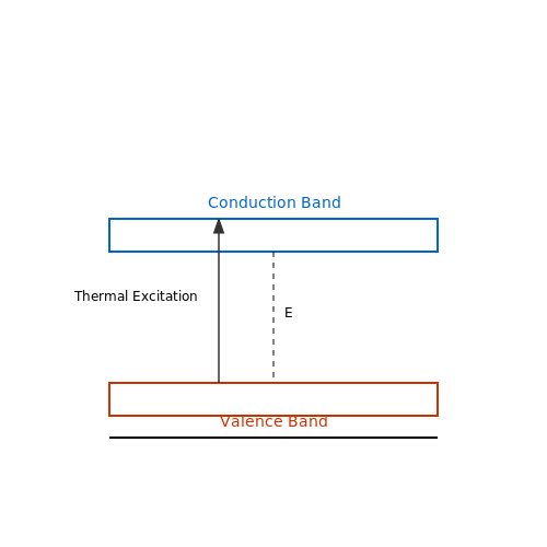
At finite temperatures, electron-hole pairs are generated through thermal excitation across the bandgap. The intrinsic carrier concentration ni determines this component of leakage current:
where Nc and Nv are the effective density of states in the conduction and valence bands, respectively, Eg is the bandgap energy, and kT is the thermal energy. In reverse-biased pn junctions, these thermally generated carriers diffuse to the depletion region edges and are swept across by the built-in field.
Defect-Assisted Tunneling
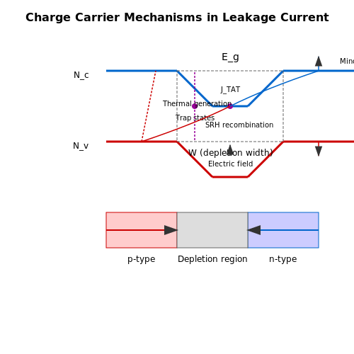
Mid-gap trap states introduced by impurities or crystal defects enable additional leakage pathways through:
- Shockley-Read-Hall (SRH) generation-recombination: Defect states act as stepping stones for carriers to traverse the bandgap with lower activation energy.
- Trap-assisted tunneling (TAT): High electric fields enable direct tunneling via defect states, with current density scaling exponentially with field strength.
where m* is the effective carrier mass and F is the electric field.
Minority Carrier Diffusion
In MOSFETs, subthreshold leakage is dominated by minority carrier diffusion from source to drain when gate voltage VGS is below threshold:
where n is the subthreshold swing factor (typically 1.0-1.5). This exponential dependence makes leakage highly sensitive to threshold voltage variations at nanometer scales.
Impact of Doping Concentration
Heavily doped regions exhibit enhanced leakage due to:
- Bandgap narrowing from many-body effects
- Increased trap state density near the band edges
- Enhanced tunneling probability through thinner potential barriers
The junction leakage current density Jleak in abrupt pn junctions follows:
where W is depletion width, τg is generation lifetime, and D/L terms represent minority carrier diffusion coefficients/lengths.
1.3 Thermal Generation and Recombination Effects
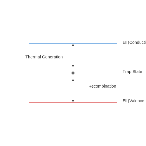
Thermal generation and recombination of charge carriers play a critical role in determining leakage currents in semiconductors. At finite temperatures, lattice vibrations (phonons) provide the energy required to break covalent bonds, generating electron-hole pairs. Conversely, recombination occurs when electrons fall back into vacant states (holes), releasing energy as phonons or photons.
Intrinsic Carrier Concentration
The equilibrium concentration of thermally generated carriers in an intrinsic semiconductor is governed by the intrinsic carrier density ni, derived from Fermi-Dirac statistics and the density of states:
where Nc and Nv are the effective densities of states in the conduction and valence bands, Eg is the bandgap energy, and kB is the Boltzmann constant. For silicon at 300 K, ni ≈ 1.5×1010 cm−3.
Generation-Recombination Kinetics
The net generation-recombination rate U under non-equilibrium conditions is described by Shockley-Read-Hall (SRH) theory:
Here, τn and τp are carrier lifetimes, while n1 and p1 are defect-level-dependent terms. In reverse-biased junctions, where np ≪ ni2, the generation rate dominates, contributing to leakage current as:
where W is the depletion width and τg is the generation lifetime.
Temperature Dependence
Leakage currents exhibit exponential temperature dependence due to the Arrhenius relationship in ni:
For silicon, leakage current typically doubles every 8–10°C rise in temperature. This effect is critical in power devices and high-temperature electronics, where Jleak can dominate power dissipation.
Practical Implications
- Dark current in image sensors arises from thermal generation in depletion regions.
- Standby power in CMOS circuits is exacerbated by subthreshold and junction leakage at elevated temperatures.
- Radiation-hardened designs minimize generation-recombination centers via defect engineering.
2. Diffusion Current in p-n Junctions
Diffusion Current in p-n Junctions
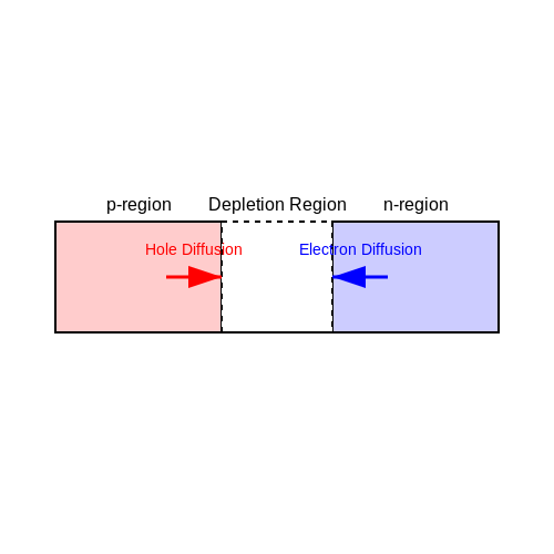
In a p-n junction, diffusion current arises due to the concentration gradient of charge carriers across the depletion region. When p-type and n-type semiconductors are brought into contact, majority carriers (holes in p-region, electrons in n-region) diffuse across the junction, recombining near the interface and establishing an equilibrium condition. This diffusion process is governed by Fick's first law, where the particle flux is proportional to the negative gradient of carrier concentration.
Mathematical Derivation of Diffusion Current
The electron diffusion current density \( J_{n,\text{diff}} \) can be expressed as:
where:
- \( q \) is the elementary charge (\(1.6 \times 10^{-19} \text{ C}\)),
- \( D_n \) is the electron diffusion coefficient,
- \( \frac{dn}{dx} \) is the electron concentration gradient.
Similarly, the hole diffusion current density is:
The negative sign indicates that holes diffuse in the opposite direction of the concentration gradient. The total diffusion current is the sum of both contributions:
Einstein Relation and Mobility
The diffusion coefficient \( D \) and carrier mobility \( \mu \) are related through the Einstein relation:
where \( k_B \) is the Boltzmann constant and \( T \) is the temperature. This relation ensures consistency between drift and diffusion mechanisms in semiconductor theory.
Practical Implications
Diffusion current dominates in forward-biased p-n junctions, where the applied voltage reduces the built-in potential barrier, allowing majority carriers to flow. In reverse bias, diffusion current becomes negligible compared to the drift current caused by minority carriers. Understanding this balance is critical in diode modeling, solar cells, and bipolar junction transistors (BJTs), where carrier transport mechanisms define device behavior.
The diagram illustrates the diffusion of holes (red) from the p-region and electrons (blue) from the n-region, forming the depletion zone where recombination occurs.
Non-Ideal Effects and Recombination
In real devices, recombination in the depletion region modifies the diffusion current. The Shockley-Read-Hall (SRH) recombination model describes this process, where trap-assisted recombination reduces the net carrier flux. High-level injection further complicates the diffusion dynamics, requiring numerical solutions in advanced semiconductor simulations.
2.2 Drift Current in Electric Fields
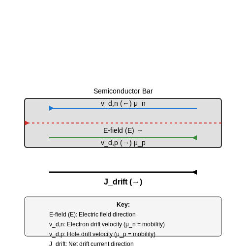
When an electric field E is applied to a semiconductor, charge carriers (electrons and holes) experience a force that drives their motion. This phenomenon, known as drift, results in a net current called drift current. The drift current density Jdrift is governed by the carrier mobility and the applied field.
Carrier Mobility and Drift Velocity
The average velocity of carriers due to the electric field is termed the drift velocity (vd). For electrons and holes, this is given by:
where μn and μp are the electron and hole mobilities, respectively. The negative sign for electrons indicates their motion opposes the field direction due to their negative charge.
Drift Current Density
The drift current density for electrons (Jn,drift) and holes (Jp,drift) is derived from the product of charge, carrier concentration, and drift velocity:
Here, q is the elementary charge, n is the electron concentration, and p is the hole concentration. The total drift current density is the sum of both contributions:
Conductivity and Resistivity
The conductivity σ of the semiconductor is directly related to the drift current:
Conversely, the resistivity ρ is the inverse of conductivity:
In extrinsic semiconductors, one carrier type dominates (e.g., electrons in n-type), simplifying the expression.
Temperature Dependence
Mobility decreases with rising temperature due to increased lattice scattering, while carrier concentration may increase (in intrinsic semiconductors). The net effect on conductivity depends on doping:
- Low-doped semiconductors: Conductivity rises with temperature (carrier concentration dominates).
- Heavily-doped semiconductors: Conductivity decreases (mobility reduction dominates).
Practical Implications
Drift current is critical in semiconductor devices:
- Ohmic contacts: Low-resistance current flow relies on high carrier mobility.
- Field-effect transistors (FETs): Channel conductivity is modulated by carrier drift under gate bias.
- Leakage paths: Unintended drift current contributes to leakage in high-field regions.
2.3 Tunneling and Band-to-Band Leakage
Quantum Tunneling in Semiconductor Junctions
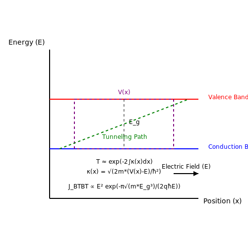
In highly doped p-n junctions or ultrathin oxide barriers (e.g., MOSFET gate dielectrics), charge carriers can traverse classically forbidden energy barriers via quantum tunneling. The tunneling probability T is derived from the Wentzel-Kramers-Brillouin (WKB) approximation:
where κ(x) is the decay constant:
Here, m* is the effective mass, V(x) the potential barrier, and E the carrier energy. For triangular barriers (e.g., reverse-biased junctions), this simplifies to Fowler-Nordheim tunneling.
Band-to-Band Tunneling (BTBT)
In narrow-bandgap semiconductors or high electric fields (>1 MV/cm), electrons from the valence band can tunnel directly into the conduction band, generating electron-hole pairs. The Kane model describes BTBT current density JBTBT:
where A and B are material-dependent constants, E the electric field, and Eg the bandgap. This mechanism dominates in tunnel FETs and contributes to leakage in sub-10nm transistors.
Practical Implications
- Gate Oxide Leakage: Direct tunneling through SiO2 layers thinner than 2nm causes standby power dissipation in CMOS devices.
- Zener Diodes: Controlled BTBT enables voltage regulation at reverse bias.
- Negative Differential Resistance: Resonant tunneling diodes exploit coherent carrier transport for high-frequency oscillators.
Mitigation Strategies
Modern devices employ:
- High-κ dielectrics (e.g., HfO2) to reduce gate leakage while maintaining capacitance.
- Strain engineering to modulate bandgaps and suppress BTBT.
- Heterojunction designs (e.g., SiGe/Si) to create tunneling barriers.
Surface and Interface Leakage Effects
Surface and interface leakage currents arise due to imperfections at semiconductor surfaces and heterojunction interfaces, often dominating bulk leakage in modern nanoscale devices. Unlike bulk leakage, which follows Shockley-Read-Hall (SRH) recombination statistics, surface leakage is governed by interface trap states, dangling bonds, and surface contamination.
Mechanisms of Surface Leakage
At the semiconductor surface, incomplete atomic bonds create mid-gap trap states that facilitate carrier generation-recombination. The leakage current density (Jsurf) can be modeled as:
where s0 is the surface recombination velocity, ni the intrinsic carrier concentration, and V the applied bias. For silicon at 300K, s0 ranges from 102 cm/s (well-passivated) to 106 cm/s (unpassivated).
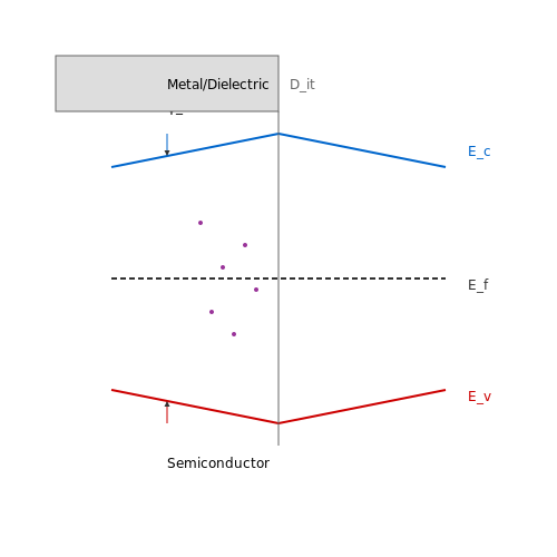
Interface Traps and Fermi-Level Pinning
At metal-semiconductor or dielectric-semiconductor interfaces, trap states pin the Fermi level, creating a conductive path. The interface trap density (Dit) directly impacts leakage:
where Cox is oxide capacitance, ψs surface potential, and φg gate voltage. High-κ dielectrics in CMOS nodes exhibit Dit > 1012 cm−2eV−1, exacerbating gate leakage.
Passivation Techniques
Effective surface passivation methods include:
- Hydrogen termination: Saturates dangling bonds (e.g., Si-H bonds reduce Dit to ~1010 cm−2eV−1).
- ALD-grown Al2O3: Provides negative fixed charge (~1013 cm−2) for field-effect passivation.
- Chalcogenide treatments: Sulfur or selenium monolayers on III-V surfaces suppress oxide regrowth.
Case Study: MOSFET Gate Leakage
In sub-10nm FinFETs, interface leakage constitutes >30% of total off-state current. TCAD simulations show that a 2× increase in Dit at the Si/SiO2 interface raises Ioff by 45%, highlighting the criticality of atomic-layer deposition (ALD) uniformity.
where A* is Richardson’s constant and φB the barrier height. Nitrided interfaces (SiON) increase φB by 0.2–0.3 eV compared to pure SiO2.
Experimental Characterization
Deep-level transient spectroscopy (DLTS) and conductance methods quantify interface traps:
- DLTS: Measures trap emission rates via capacitance transients.
- Split C-V: Extracts Dit from low-frequency capacitance dispersion.
3. Leakage in MOSFETs and CMOS Circuits
3.1 Leakage in MOSFETs and CMOS Circuits
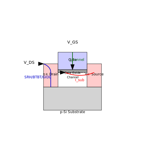
Leakage current in MOSFETs arises primarily due to subthreshold conduction, gate oxide tunneling, and junction leakage. In modern CMOS technologies, leakage becomes a dominant factor in power dissipation as transistor dimensions shrink below the 100 nm regime. Understanding its mechanisms is critical for low-power IC design.
Subthreshold Leakage
When VGS < Vth, the MOSFET operates in weak inversion, yet a small drain current Isub flows. This subthreshold current follows an exponential relationship:
where I0 depends on mobility and device geometry, n is the subthreshold swing coefficient (typically 1.3–1.8), and VT = kT/q is the thermal voltage. At room temperature, a 100 mV reduction in Vth increases Isub by nearly 10×.
Gate Oxide Tunneling
As oxide thickness scales below 2 nm, direct tunneling of carriers through the gate dielectric becomes significant. The tunneling current density Jtunnel follows the Fowler-Nordheim model:
where Eox is the oxide electric field and β is a material-dependent constant. High-κ dielectrics like HfO2 mitigate this by achieving equivalent oxide thickness (EOT) with physically thicker layers.
Junction Leakage
Reverse-biased source/drain junctions exhibit leakage due to:
- Shockley-Read-Hall (SRH) generation: Electron-hole pair generation in the depletion region
- Band-to-band tunneling (BTBT): Significant in heavily doped junctions at high fields
- Gate-induced drain leakage (GIDL): Enhanced by high drain-to-gate voltage gradients
CMOS Circuit Implications
In static CMOS logic, leakage manifests as:
- Standby power: Cumulative leakage paths between VDD and GND
- Data retention loss: In SRAM cells, leakage necessitates periodic refresh
- Temperature dependence: Leakage currents typically double every 10°C rise
Advanced mitigation techniques include:
- Multi-threshold CMOS (MTCMOS) designs using high-Vth sleep transistors
- Dynamic voltage and frequency scaling (DVFS)
- Power gating with header/footer switches
3.2 Leakage in Diodes and Bipolar Transistors
Reverse-Bias Leakage in PN Junctions
The dominant leakage mechanism in diodes under reverse bias is generation-recombination current in the depletion region. The Shockley-Read-Hall (SRH) theory predicts the leakage current density as:
where q is the electron charge, ni the intrinsic carrier concentration, W the depletion width, and τeff the effective carrier lifetime. This current exhibits temperature dependence through ni:
Surface Leakage Components
Practical diodes show additional leakage from surface states at the junction periphery. The surface recombination velocity S0 modifies the effective lifetime:
Modern passivation techniques using silicon nitride or thermal oxides can reduce S0 to below 10 cm/s.
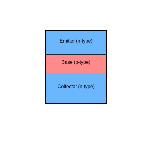
Bipolar Transistor Leakage Paths
In bipolar transistors, leakage manifests through several mechanisms:
- Collector-base leakage (ICB0): Similar to diode reverse leakage, dominant at low VCE
- Emitter-base leakage (IEB0): Becomes significant in inverse-active mode
- Surface inversion channels: Along oxide interfaces in modern shallow-junction devices
Gummel-Poon Model Extension
The complete transistor leakage appears in the Gummel-Poon model as:
High-Temperature Behavior
At elevated temperatures (>125°C), leakage currents in silicon devices typically double every 8-10°C. This follows from the exponential temperature dependence of ni. For power devices, this creates thermal runaway risks when:
where Rth is the thermal resistance. Modern TCAD tools use coupled electro-thermal simulations to predict these effects.
Measurement Techniques
Accurate leakage measurement requires:
- Guarded test structures to eliminate surface conduction
- Temperature-controlled probe stations (±0.1°C stability)
- Femtoampere-resolution source-measure units
- Dark-box shielding for photocurrent suppression
The Y-factor method using two temperature points can separate bulk and surface components.
3.3 Power Dissipation and Heat Generation
Leakage current in semiconductors contributes directly to power dissipation, which manifests as heat generation. Even in the absence of active switching, leakage currents—primarily subthreshold and gate oxide leakage—result in a continuous power loss given by:
where Ileak is the aggregate leakage current and VDD is the supply voltage. For modern CMOS devices, this static power dissipation becomes significant at nanoscale nodes due to exponential increases in leakage with shrinking oxide thicknesses.
Thermal Implications
The generated heat raises the junction temperature (Tj), which further exacerbates leakage due to the temperature dependence of carrier mobility and intrinsic carrier concentration (ni). The relationship is captured by:
where Eg is the bandgap energy and kB is the Boltzmann constant. This positive feedback loop can lead to thermal runaway in poorly designed systems.
Practical Mitigation Strategies
- Dynamic Voltage and Frequency Scaling (DVFS): Reduces VDD during low-activity periods to curb leakage power.
- Power Gating: Disconnects unused blocks from the supply voltage using high-Vth sleep transistors.
- Thermal-Aware Design: Incorporates heat sinks, thermal vias, and advanced packaging to dissipate heat efficiently.
Case Study: FinFET Leakage Reduction
FinFET architectures reduce leakage by 10–100× compared to planar CMOS at equivalent nodes, owing to improved gate control over the channel. The 3D gate structure suppresses short-channel effects, lowering subthreshold leakage (Ioff). However, gate-induced drain leakage (GIDL) becomes a dominant factor at sub-10nm nodes, requiring careful optimization of fin geometry and strain engineering.
4. Current-Voltage (I-V) Characterization
4.1 Current-Voltage (I-V) Characterization
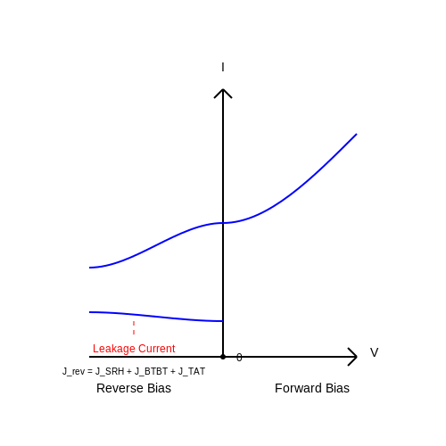
The current-voltage (I-V) characteristics of a semiconductor device provide critical insights into its leakage behavior, particularly under reverse and forward bias conditions. Leakage current manifests as an undesirable conduction path, often due to minority carrier diffusion, trap-assisted tunneling, or defect-mediated conduction.
Reverse-Bias Leakage Current
Under reverse bias, the dominant leakage mechanisms are:
- Shockley-Read-Hall (SRH) generation-recombination: Defect states in the forbidden gap facilitate carrier generation, contributing to reverse leakage.
- Band-to-band tunneling (BTBT): High electric fields induce direct tunneling of electrons from the valence to conduction band.
- Trap-assisted tunneling (TAT): Defects act as stepping stones for carriers tunneling through the bandgap.
The reverse leakage current density \( J_{rev} \) can be modeled as:
Forward-Bias Leakage Current
Under forward bias, leakage is typically overshadowed by the exponential increase in diffusion current. However, at low voltages, the following mechanisms contribute:
- Surface recombination: Unpassivated surfaces introduce trap states that enhance leakage.
- Parasitic shunt paths: Crystalline defects or metallic precipitates create low-resistance conduction paths.
I-V Measurement Techniques
Accurate I-V characterization requires:
- Guarded measurements: Eliminates surface leakage by isolating the bulk current path.
- Temperature-controlled probing: Leakage currents often exhibit Arrhenius dependence, making temperature a critical parameter.
- Low-noise instrumentation: Sub-picoamp sensitivity is necessary for modern nanoscale devices.
Practical Implications
In MOSFETs, gate leakage due to direct tunneling increases exponentially with oxide thinning. For power devices, leakage determines standby power consumption and breakdown robustness. Advanced materials like high-k dielectrics and wide-bandgap semiconductors (SiC, GaN) are engineered specifically to minimize leakage.
4.2 Temperature-Dependent Leakage Analysis
Thermally Activated Leakage Mechanisms
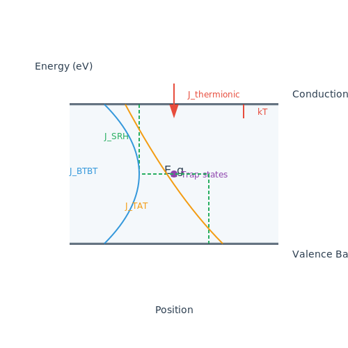
Leakage current in semiconductors exhibits strong temperature dependence due to the thermal activation of charge carriers. The primary mechanisms contributing to temperature-dependent leakage include:
- Shockley-Read-Hall (SRH) generation-recombination
- Band-to-band tunneling (BTBT)
- Trap-assisted tunneling (TAT)
- Thermionic emission over potential barriers
The total leakage current density Jleak can be expressed as the sum of these components:
Mathematical Modeling of Temperature Dependence
The temperature dependence of SRH generation-recombination current follows an Arrhenius relationship:
where q is the electron charge, ni is the intrinsic carrier concentration, W is the depletion width, τeff is the effective carrier lifetime, Eg is the bandgap energy, k is Boltzmann's constant, and T is absolute temperature.
The intrinsic carrier concentration ni itself has a strong temperature dependence:
Bandgap Narrowing Effects
At elevated temperatures, the semiconductor bandgap Eg decreases according to the Varshni equation:
where Eg(0) is the bandgap at 0 K, and α and β are material-specific constants. For silicon:
- α ≈ 4.73 × 10⁻⁴ eV/K
- β ≈ 636 K
Practical Implications for Device Design
The exponential temperature dependence of leakage currents has critical implications:
- Power dissipation: Leakage power can dominate total power consumption at high temperatures
- Reliability: Elevated temperatures accelerate time-dependent dielectric breakdown (TDDB)
- Circuit performance: Leakage variability affects timing margins and noise immunity
Modern CMOS technologies implement several mitigation strategies:
- High-k gate dielectrics to reduce direct tunneling
- Strained silicon to maintain carrier mobility at reduced voltages
- Dynamic voltage and frequency scaling (DVFS) to limit temperature rise
Measurement Techniques
Characterizing temperature-dependent leakage requires careful experimental methods:
where Ea is the activation energy extracted from Arrhenius plots. Measurement considerations include:
- Precise temperature control (±0.1°C stability)
- Elimination of parasitic thermoelectric effects
- Correction for series resistance variations
4.3 Advanced Techniques: DLTS and Noise Spectroscopy
Deep-Level Transient Spectroscopy (DLTS)
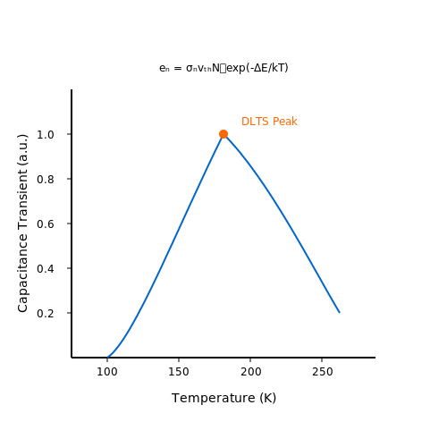
Deep-Level Transient Spectroscopy (DLTS) is a high-resolution technique for characterizing trap states in semiconductors. It measures the thermal emission of carriers from deep-level defects by analyzing capacitance transients induced by a periodic filling pulse. The time constant of the transient is temperature-dependent, allowing extraction of activation energies and capture cross-sections.
Where en is the emission rate, NT,i is the trap concentration, and ND is the doping density. The emission rate follows an Arrhenius relationship:
DLTS systems typically use a double-boxcar averaging method to isolate specific emission rates. Modern implementations employ lock-in amplification or Fourier transform techniques for improved sensitivity below 1010 cm-3 trap concentrations.
Noise Spectroscopy
Low-frequency noise (LFN) spectroscopy probes defect dynamics through voltage or current fluctuations. Two primary noise mechanisms reveal leakage paths:
- Generation-recombination (G-R) noise: Arises from carriers trapped and released by defects, producing Lorentzian spectra
- 1/f noise: Results from distributed time constants at interfaces or bulk defects
The spectral density of G-R noise follows:
where τ is the defect time constant and ΔV is the fluctuation amplitude. Noise measurements at varying temperatures map defect energies through the relationship:
Comparative Analysis
DLTS provides superior energy resolution (±5 meV) but requires Schottky contacts. Noise spectroscopy works with two-terminal devices and detects defects influencing conduction paths directly. Combined approaches resolve conflicts between electrically active versus recombination-active defects.
Practical Applications
- Identifying gate leakage mechanisms in MOSFETs through interface trap characterization
- Quantifying bulk defects in power devices using temperature-dependent DLTS scans
- Correlating 1/f noise with reliability metrics in advanced FinFET nodes
5. Material Engineering for Reduced Leakage
5.1 Material Engineering for Reduced Leakage
Bandgap Engineering for Leakage Suppression
Leakage current in semiconductors is strongly influenced by the material's bandgap (Eg). A wider bandgap reduces intrinsic carrier concentration (ni), which follows:
where Nc and Nv are the effective density of states in the conduction and valence bands, respectively. High-k dielectrics like HfO2 (Eg ≈ 5.7 eV) reduce gate leakage by orders of magnitude compared to SiO2 (Eg ≈ 8.9 eV).
Strain Engineering Techniques
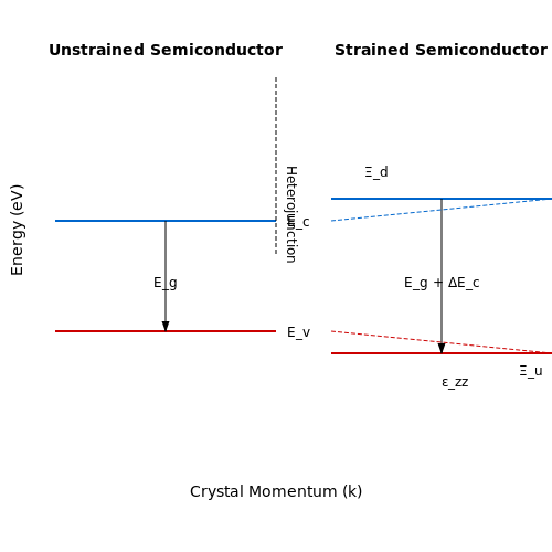
Applied strain modifies the band structure through deformation potentials. Biaxial tensile strain in silicon:
- Increases electron mobility by reducing intervalley scattering
- Raises the conduction band minimum, increasing the effective bandgap
- Reduces band-to-band tunneling (BTBT) leakage
The strain-induced band shift can be quantified as:
where Ξd and Ξu are deformation potentials, and ε is the strain tensor.
Advanced Channel Materials
Compound semiconductors provide superior leakage characteristics:
| Material | Bandgap (eV) | Leakage Reduction Factor |
|---|---|---|
| Si | 1.12 | 1× (reference) |
| Ge | 0.66 | 10× worse |
| GaAs | 1.42 | 5× better |
| GaN | 3.4 | 100× better |
Interface Engineering
Abrupt heterojunctions create quantum confinement that suppresses leakage. The transmission probability T through a potential barrier is given by:
Graded AlxGa1-xAs junctions (x: 0 → 0.3 over 10 nm) demonstrate 40% lower leakage than abrupt interfaces in HEMTs.
Defect Passivation Methods
Mid-gap states from dangling bonds act as generation-recombination centers. Hydrogen passivation of Si/SiO2 interfaces reduces interface trap density (Dit) from 1012 to 1010 cm-2eV-1. Advanced techniques include:
- Plasma-enhanced atomic layer deposition (PE-ALD) for conformal passivation
- Fermi-level pinning mitigation using rare-earth oxides
- Chalcogenide termination of III-V surfaces
5.2 Device Design Optimization
Minimizing leakage current in semiconductor devices requires careful optimization of material properties, geometric parameters, and operating conditions. The dominant mechanisms—subthreshold conduction, gate-induced drain leakage (GIDL), and junction leakage—must be addressed through targeted design strategies.
Channel Doping Profile Engineering
Precise control of channel doping concentration (Na or Nd) directly impacts subthreshold swing (S), given by:
where Cdep is the depletion capacitance and Cox the oxide capacitance. Retrograde doping profiles, with higher concentration near the substrate, reduce junction leakage while maintaining low threshold voltage. Halos or pocket implants near source/drain junctions suppress short-channel effects without increasing off-state current.
Gate Stack Optimization
The gate dielectric thickness (tox) and material selection critically influence direct tunneling current, which follows the form:
High-κ dielectrics (HfO2, Al2O3) allow thicker physical layers while maintaining equivalent oxide thickness (EOT). Metal gate work function engineering (Φm) enables precise threshold voltage tuning without resorting to excessive channel doping that would increase junction leakage.
Source/Drain Design
Abrupt junction profiles minimize generation-recombination leakage, requiring advanced annealing techniques like laser spike annealing (LSA) or flash lamp annealing (FLA). Elevated source/drain structures reduce parasitic resistance while allowing deeper junctions that suppress punchthrough. Strain engineering through SiGe or stress liners improves mobility without increasing leakage paths.
Voltage and Temperature Considerations
Operating voltage scaling follows the empirical relationship for leakage power density:
where W is device width and N the number of devices. Multi-threshold voltage (multi-Vth) designs allow critical paths to use low-Vth transistors while leakage-dominated blocks employ high-Vth devices. Temperature-aware design must account for the exponential dependence of leakage on junction temperature (Tj):
Advanced packaging solutions such as 3D ICs with microfluidic cooling can maintain Tj below 85°C even in high-power-density designs.
5.3 Circuit-Level Leakage Reduction Techniques
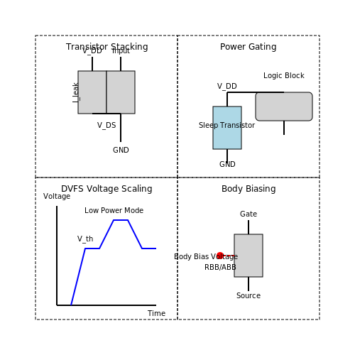
Leakage current in semiconductor devices arises from subthreshold conduction, gate oxide tunneling, and reverse-biased junction currents. At the circuit level, several techniques mitigate these effects while maintaining performance. These methods exploit transistor stacking, dynamic threshold control, and power gating to minimize leakage without compromising functionality.
Transistor Stacking Effect
When multiple transistors are stacked in series, the intermediate nodes settle at voltages above ground, reducing the drain-to-source voltage (VDS) of each transistor. This effect decreases subthreshold leakage due to the dependence of leakage current on VDS:
For a two-transistor stack, the leakage reduction factor (K) is empirically derived as:
where Vth is the threshold voltage, n is the subthreshold swing coefficient, and VT is the thermal voltage. Stacking three or more transistors further amplifies this effect but introduces trade-offs in delay and area.
Dynamic Voltage and Frequency Scaling (DVFS)
DVFS adjusts supply voltage (VDD) and clock frequency dynamically based on workload demands. Since leakage current scales exponentially with VDD:
reducing VDD during idle periods curbs leakage power quadratically. Modern processors implement DVFS through adaptive clock generators and switched-capacitor voltage regulators, achieving up to 60% leakage reduction in low-power modes.
Power Gating with Sleep Transistors
High-Vth sleep transistors disconnect idle circuit blocks from the power supply, reducing both active and standby leakage. The sleep transistor's sizing is critical:
where Imax is the maximum current during wake-up, twake-up is the transition time, and Cox is the gate oxide capacitance. Fine-grained power gating partitions circuits into smaller domains to minimize wake-up energy overhead.
Reverse Body Biasing (RBB)
Applying a negative bias to the substrate increases the threshold voltage, suppressing subthreshold leakage. The body effect is modeled as:
where γ is the body-effect coefficient and φF is the Fermi potential. RBB is particularly effective in FD-SOI (Fully Depleted Silicon-on-Insulator) technologies, where the buried oxide layer enhances bias control.
Multi-Threshold CMOS (MTCMOS)
MTCMOS combines high-Vth transistors for power gating with low-Vth transistors in critical paths. The optimal high-Vth is derived from the leakage-delay trade-off:
where ΔV = nVT. MTCMOS is widely used in SRAM bitcells and clock networks to preserve performance while minimizing standby power.
Adaptive Body Biasing (ABB)
ABB dynamically adjusts Vth to compensate for process variations. A feedback loop measures circuit delay and tunes the body bias to maintain optimal leakage. The control law for ABB is:
where KP and KI are proportional and integral gains. ABB reduces leakage spread across dies by 3–5× in advanced nodes.
6. Key Research Papers and Books
6.1 Key Research Papers and Books
- PDF Full-Chip Analysis of Leakage Power Under Process Variations, Including ... — of subthreshold and gate leakage currents and their interactions are considered. We will loosely use the terms "leakage current" and "leakage power" interchangeably, since the two terms are related by a multiplicative factor of . 3.1 Static Leakage Models 3.1.1 SubthresholdLeakage Model The subthreshold leakage current, dent on the ...
- Full-chip leakage analysis for 65 nm CMOS technology and beyond — In current CMOS technology, the major leakage components include subthreshold leakage (I sub), gate tunneling leakage (I gate), and reverse biased junction tunneling leakage (I junc) in drain-substrate and source-substrate junctions [4].For a drawn gate length (L drawn) before the 90 nm CMOS technology, the junction tunneling leakage current is typically very small, while I sub and I gate ...
- PDF Comparative Analysis & Study of Various Leakage Reduction ... - Springer — Subthreshold leakage current depends on the channel length,gateoxidethickness,thresholdvoltage,dopingprofile, supply voltage and junction depth. This leakage current is negligible in long channel devices but is a dominant factor in submicron devices. In Junctionless transistors, sub thresh-old leakage is the main source of power loss in the OFF ...
- Leakage Current and Thermal Effects - ScienceDirect — In BSIM-IMG model the short-channel effects have been accurately modeled as described in Chapter 3, Channel Current Model With Real Device Effects in BSIM-IMG.Short-channel effect formulation for the drain-induced barrier lowering (DIBL), threshold voltage roll-off, and subthreshold slope degradation include parameters that can be used to accurately model the subthreshold drain-source leakage ...
- (PDF) A Voltage-Based Leakage Current Calculation Scheme and its ... — The key poi nt of the above ... research papers and a textbook in three volumes. ... K. Sharma et al. proposes a methodology based on Boolean logic in order to reduce leakage current while taking ...
- Leakage current mechanisms and leakage reduction techniques in deep ... — The surprisingly low leakage current density of SHO is ascribed to the large bandgap (≈6 eV), the large conduction band offset (CB offset > 3 eV) with respect to the semiconductor, and the low ...
- Leakage Reduction - SpringerLink — The usage of low leakage transistors that have high threshold voltages (HVT), in series with the supply voltage, is a well-known technique used to reduce the leakage current of the logic gates in a certain block . An HVT pMOS device can be used in series with the "logic 1 supply voltage (V dd)" to
- PDF DEGRADATION IN SILICON CARBIDE SCHOTTKY POWER DIODES Robert A. Johnson ... — RELIABILITY CHARACTERIZATIONS OF ION-INDUCED LEAKAGE CURRENT DEGRADATION IN SILICON CARBIDE SCHOTTKY POWER DIODES By Robert A. Johnson III ... Research Grants Program, and the NASA Electronic Parts and Packaging Program. Finally, I would like to thank my parents, whose effort to see that I do well every step of my life I ...
- Improvement of Leakage Current in Double Pocket FDSOI 22 nm Transistor ... — Silicon technologies have grown every year with high speed. The major obstacle that must be concentrate with silicon technologies is impacts of decreasing dimensions of devices [].The better device performance and from head to foot integration density can be achieved by scaling down of the devices [].Leakage current and short channel effects are major problem that downgrades the device ...
- Leak-Gauge: A late-mode variability-aware leakage power estimation ... — We propose a complete framework for estimation of full-chip leakage power distributions in presence of process variation. While as a late-mode estimation framework, we primarily aim for accuracy and use a Monte Carlo based approach as opposed to popular statistical methods, the components of the framework are designed in a way that only a minimal timing penalty is imposed on the flow of system ...
6.2 Online Resources and Tutorials
- Microelectronic Devices and Circuits - MIT OpenCourseWare — 6.012 is the header course for the department's "Devices, Circuits and Systems" concentration. The topics covered include modeling of microelectronic devices, basic microelectronic circuit analysis and design, physical electronics of semiconductor junction and MOS devices, relation of electrical behavior to internal physical processes, development of circuit models, and understanding the uses ...
- PDF Full-Chip Analysis of Leakage Power Under Process Variations, Including ... — ABSTRACT In this paper, we present a method for analyzing the leakage cur-rent, and hence the leakage power, of a circuit under process param-eter variations that can include spatial correlations due to intra-chip variation. A lognormal distribution is used to approximate the leak-age current of each gate and the total chip leakage is determined by summing up the lognormals. In this work, Both ...
- PDF Chapter 6 Extrinsic Semiconductors - IIT Delhi — a hole in the defect energy level. And for the Acceptor case, it is the probability of filling an electron into the acceptor energy level. Now, with these equations, it becomes easy to see the effect of temperature on the actual carrier concentration at different dopign levels. gA is the degeneracy level of the hole, which is number of spins*number of bands (2*2). gD is the same definition for ...
- PDF The Semiconductor Module User s Guide - COMSOL Multiphysics — The Semiconductor Branch Interface chapter includes physics feature information and describes the theory relating to The Semiconductor Interface. Topics include The Sommerfeld Model and the Density of States, Electrons in a Perturbed Periodic Potential, Equilibrium Carrier Concentrations, Band Gap Narrowing, and many others.
- PDF Low-Power CMOS Circuits: Technology, Logic Design and CAD Tools — 13.2 Leakage Components metal-oxide semiconductor fluid-effect transistor (MOSFET) of the nanometer regime has three dominant components of leakage: Subthreshold leakage, which is the leakage current from drain to source (I sub in Figure 13.1).
- Semiconductor Devices: Theory and Application - Open Textbook Library — The goal of this text, as its name implies, is to allow the reader to become proficient in the analysis and design of circuits utilizing discrete semiconductor devices. It progresses from basic diodes through bipolar and field effect transistors. The text is intended for use in a first or second year course on semiconductors at the Associate or Baccalaureate level. In order to make effective ...
- Leakage Reduction | SpringerLink — The usage of low leakage transistors that have high threshold voltages (HVT), in series with the supply voltage, is a well-known technique used to reduce the leakage current of the logic gates in a certain block [40].
- PDF Introduction to the Semiconductor Module - COMSOL Multiphysics — Introduction Device engineers and physicists use the Semiconductor Module to design and optimize semiconductor devices. For many years semiconductor device design has been closely associated with the use of simulation tools, due to the high cost of prototyping new devices and processes.
- PDF The Semiconductor Module User s Guide - COMSOL Multiphysics — The Semiconductor Module includes an additional Semiconductors material database with material properties appropriate for several materials. For detailed information about materials and the Semiconductor Material Library, see Materials in the COMSOL Multiphysics Reference Manual.
- PDF Fundamentals of Semiconductors: Physics and Materials Properties, 4th ... — Although semiconductor physics is covered to some extent in all advanced textbooks on condensed matter physics, the treatment rarely provides the level of detail satisfactory to research students. Well-established books on semiconductor physics are often found to be too theoretical by ex- perimentalists and engineers.
6.3 Advanced Topics for Further Study
- PDF Suppression of Surface Leakage Currents in InAs Avalanche Photodiodes ... — leakage currents in various III-V semiconductor-based devices [23-27]. For example, He et al.[27] have investigated the effect of Al 2O 3 passivation layer on the interface electrical properties of MOS capacitors fabricated using HfTiO as the dielectric on InGaAs, resulting in low leakage current of 1.17 x 10⁻⁵ A/cm2 at an applied gate voltage ...
- 7 MOSFETs in ICs-Scaling, Leakage, and Other Topics - Academia.edu — The drain voltage can pull the potential 277 Hu_ch07v3.fm Page 278 Friday, February 13, 2009 4:55 PM 278 Chapter 7 MOSFETs in ICs—Scaling, Leakage, and Other Topics S D Cg Cd Leakage path FIGURE 7-13 The drain could still have more control than the gate along another leakage current path that is some distance below the Si surface.
- Leakage Current - an overview | ScienceDirect Topics — The gate leakage current was found to be one of the possible causes for the signal drop often observed close to the threshold. Results of calculations 27 for different values of leakage currents are shown in Fig. 5.11.One can see that for a low leakage current the signal increases and reaches the same saturation value. This value is given by Equation [5.26].
- PDF MOSFETs in ICs—Scaling, Leakage, and Other Topics - Chenming Hu — MOSFETs in ICs—Scaling, Leakage, and Other Topics CHAPTER OBJECTIVES How the MOSFET gate length might continue to be reduced is the subject of this chap-ter. One important topic is the off-state current or the leakage current of the MOSFETs. This topic complements the discourse on the on-state current conducted in the previ-ous chapter.
- Short-Channel Effects in MOSFETs - SpringerLink — The oxide thickness at which direct tunneling starts is 3 nm. With reduction of gate oxide thickness, direct quantum-mechanical tunneling of electrons from the gate across the gate oxide to the underlying silicon causes an increase in the gate leakage current. The gate leakage current density = 100 Acm −2 at 1 V for 1.2 nm thick oxide. After ...
- Quantitative prediction of junction leakage in bulk-technology CMOS ... — The International Technology Roadmap for Semiconductors [1] (ITRS) specifies leakage targets for current and future generation MOS technologies. Literature on diode leakage has been available for many decades now. However there are a number of aspects of modern MOS device processing and design that necessitate an updated study on junction leakage.
- PDF Fundamentals of Semiconductors: Physics and Materials Properties, 4th ... — Physics for the year 2000 has been awarded to two semiconductor physicists, Zhores I. Alferov and Herbert Kroemer ("for developing semiconductor het-erostructures used in high-speed- and opto-electronics") and a semiconductor device engineer, Jack S. Kilby ("for his part in the invention of the integrated circuit").
- Leakage Reduction - SpringerLink — From (), we conclude that the leakage current increases exponentially with decreasing threshold voltage (V t).It also scales linearly with the transistor width (W), exponentially with thermal voltage (v t), and has a complex relationship with the channel length l.On one hand, it has a linear relation with the reciprocal of channel length for long channel MOS, but due to short channel effect ...
- Nanoscale Effects: Gate Oxide Leakage Currents — As MOSFETs are scaled down to nanoscale, QMEs need to be considered in MOSFET design and modeling. In today's CMOS technology, the gate oxide thickness of a MOSFET is less than 1.5 nm, and the channel is doped as high as 1×10 18 cm −3.For MOSFETs with heavily doped channels and ultrathin oxide layers, the field in the oxide can reach very high values of MV/cm.
- (PDF) Gate Leakage and Threshold Voltage Dynamics in MOSFETs - Academia.edu — An Anomalous Correlation between Gate Leakage Current and Threshold Voltage Fluctuation in Advanced MOSFETs Zihong Liu,1 Paul Chang,2 Xiaojun Yu,2 Jie Deng,2 Shu-Jen Han,2 Ghavam Shahidi,1 Wilfried Haensch,1 Ken Rim2 1 IBM T.J. Watson Research Center, Yorktown Heights, NY 10598 USA IBM Semiconductor Research and Development Center, Hopewell ...