Zinc Oxide Nanostructures in Electronics
1. Crystal Structure and Bandgap Properties
1.1 Crystal Structure and Bandgap Properties
Wurtzite Crystal Structure
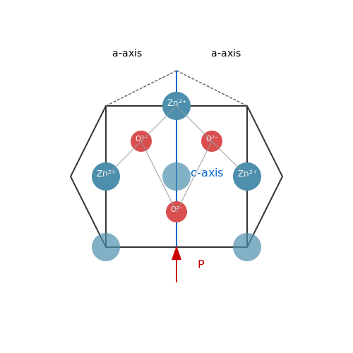
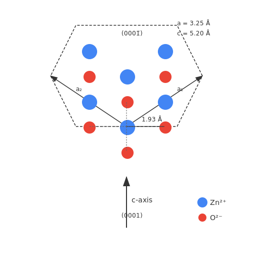
Zinc oxide (ZnO) crystallizes primarily in the wurtzite structure, a hexagonal lattice system belonging to the P63mc space group. The unit cell consists of alternating Zn2+ and O2− layers arranged in an ABAB... stacking sequence along the c-axis. Each Zn atom is tetrahedrally coordinated with four O atoms, and vice versa, with a bond length of approximately 1.93 Å. The lattice parameters are:
The wurtzite structure exhibits polar surfaces, most notably the (0001) Zn-terminated and (000$$\bar{1}$$) O-terminated planes, which influence piezoelectric and pyroelectric properties. This anisotropy is critical for nanostructure growth, as it favors directional growth along the c-axis, forming nanowires or nanorods.
Electronic Band Structure
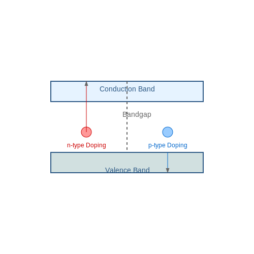
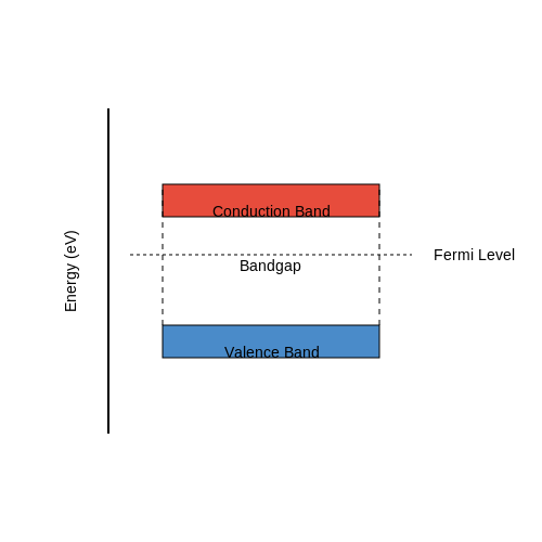
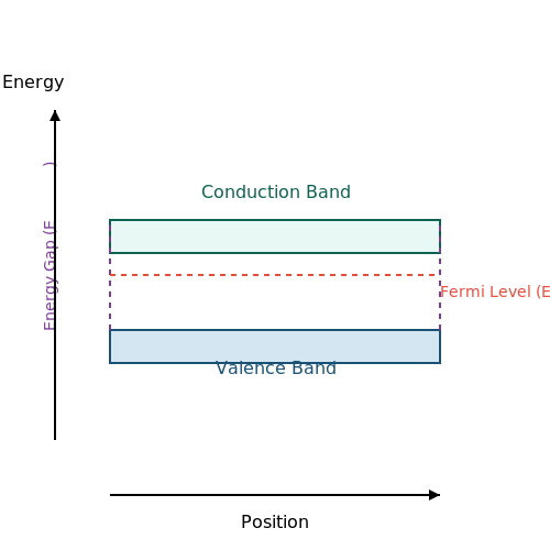
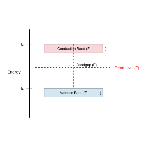
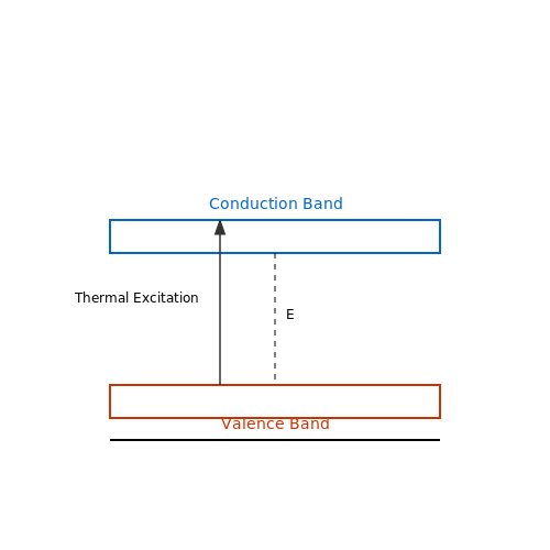
ZnO is a direct bandgap semiconductor with the valence band maximum (VBM) and conduction band minimum (CBM) both located at the Γ-point in the Brillouin zone. The bandgap energy (Eg) at room temperature is:
The bandgap arises from hybridization of Zn 3d and O 2p orbitals, with the VBM dominated by O 2p states and the CBM by Zn 4s states. Spin-orbit coupling splits the valence band into three subbands (A, B, and C) with energy separations of a few meV.
Bandgap Engineering
The bandgap can be tuned via:
- Alloying: Mg or Cd substitution modulates Eg (e.g., Zn1−xMgxO achieves Eg up to 4.0 eV).
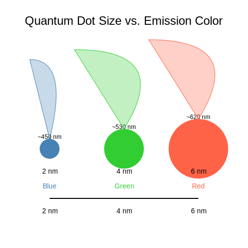
- Quantum confinement: In nanostructures (e.g., quantum dots), Eg increases due to spatial carrier confinement:
where R is the nanostructure radius and μ the reduced effective mass.
Defect States and Doping
Native point defects (e.g., Zn interstitials, O vacancies) introduce shallow or deep levels within the bandgap. For instance:
- O vacancies (VO) create donor levels ~0.3 eV below CBM, enabling n-type conductivity.
- Zn vacancies (VZn) form acceptor levels ~0.8 eV above VBM, though p-type doping remains challenging.
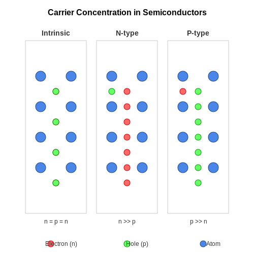
Intentional doping with group-III (Al, Ga) or group-V (N, P) elements enhances carrier concentrations for device applications like transparent conductive oxides (TCOs) or UV photodetectors.
Optical and Electronic Applications
The wide bandgap and exciton binding energy (~60 meV) make ZnO suitable for:
- UV optoelectronics: LEDs and lasers exploiting near-band-edge emission at ~380 nm.
- Piezotronics: Strain-gated transistors leveraging piezoelectric polarization charges.
- Heterostructures: Type-II band alignment with materials like Cu2O for photovoltaic applications.
Recent advances include ZnO nanowire arrays for flexible electronics, where the wurtzite structure’s mechanical robustness complements its electronic properties.
1.2 Electrical and Optical Characteristics
Electrical Properties
Zinc oxide (ZnO) nanostructures exhibit unique electrical properties due to their wide bandgap (~3.37 eV at room temperature) and high exciton binding energy (~60 meV). The conductivity of ZnO can be tuned via doping, with common dopants including Al, Ga, and In for n-type conductivity, and N, P, and As for p-type conductivity. The carrier concentration (n) and mobility (μ) in ZnO nanostructures are governed by:
where σ is the electrical conductivity and e is the electron charge. For undoped ZnO, the intrinsic carrier concentration is low (~106 cm−3), but doping can increase this to >1020 cm−3.
Optical Properties
ZnO nanostructures exhibit strong near-band-edge (NBE) emission in the ultraviolet (UV) region (~375 nm) due to excitonic recombination, along with a broad visible emission band (~500–600 nm) attributed to defects such as oxygen vacancies (VO) and zinc interstitials (Zni). The photoluminescence (PL) spectrum can be modeled using:
where I(E) is the emission intensity, Eg is the bandgap energy, and kT is the thermal energy.
Piezoelectric and Pyroelectric Effects
ZnO's non-centrosymmetric wurtzite structure gives rise to strong piezoelectric and pyroelectric effects. The piezoelectric coefficient (d33) for ZnO nanowires can reach ~12 pC/N, enabling applications in nanogenerators and strain sensors. The polarization (P) under strain (ε) is given by:
where Y is Young's modulus (~140 GPa for ZnO).
Applications in Optoelectronics
ZnO nanostructures are used in UV photodetectors, light-emitting diodes (LEDs), and transparent conductive oxides (TCOs). For example, Al-doped ZnO (AZO) films achieve resistivities as low as 10−4 Ω·cm with >85% optical transparency in the visible spectrum.
Quantum Confinement Effects
In quantum dots (QDs) or ultrathin nanowires (<10 nm diameter), quantum confinement shifts the bandgap (Eg) according to:
where R is the radius of the QD, and me* and mh* are the effective masses of electrons and holes, respectively.
1.3 Synthesis Methods for ZnO Nanostructures
Vapor-Phase Transport Deposition
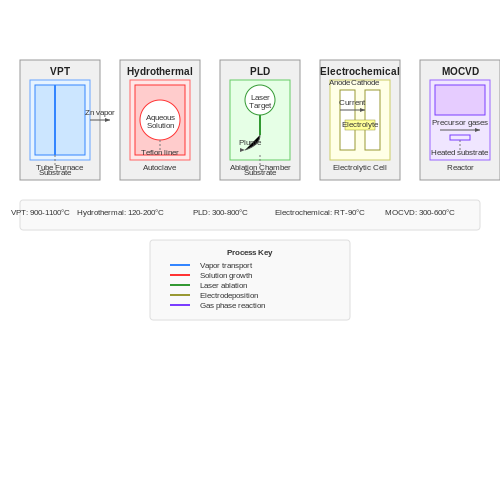
Vapor-phase transport (VPT) is a widely used method for synthesizing high-purity ZnO nanostructures. The process involves heating zinc powder (typically 90–99.99% purity) in a tube furnace at temperatures between 900–1100°C under a controlled argon or nitrogen flow (10–100 sccm). The zinc vapor reacts with oxygen to form ZnO nuclei, which subsequently grow into nanostructures on a substrate placed downstream. The growth kinetics can be described by the modified Hertz-Knudsen equation:
where J is the zinc flux, α is the sticking coefficient (0.1–0.9 for most substrates), PZn is the zinc vapor pressure, mZn is the atomic mass of zinc, and T is the temperature. This method produces nanowires with diameters of 20–200 nm and aspect ratios exceeding 50:1.
Hydrothermal Synthesis
Hydrothermal growth occurs in aqueous solutions containing zinc precursors (e.g., Zn(NO3)2 or Zn(CH3COO)2) and mineralizers (NaOH, NH4OH) at 60–200°C. The reaction proceeds through:
Crystal morphology is controlled by adjusting pH (9–12), precursor concentration (0.01–0.5 M), and reaction time (1–24 hours). This method yields nanorods with c-axis orientation and hexagonal facets due to the wurtzite structure's (0001) polar surface energy minimization.
Pulsed Laser Deposition (PLD)
PLD utilizes a KrF excimer laser (λ = 248 nm, 2–10 J/cm2) to ablate a ZnO target in an oxygen background pressure (10-6–10-1 Torr). The plasma plume's expansion dynamics follow:
where n(r,t) is the particle density at distance r and time t, and σ(t) is the plume width. Substrate temperature (300–800°C) critically affects stoichiometry, with lower temperatures favoring oxygen vacancies (VO) that enhance n-type conductivity.
Electrochemical Deposition
Electrodeposition from zinc nitrate solutions (0.1 M Zn(NO3)2, pH 6.5) at potentials of -0.8 to -1.2 V vs. Ag/AgCl follows a 4-electron process:
The current density (0.1–5 mA/cm2) controls nucleation density, with higher currents producing smaller grain sizes. This method enables low-temperature growth (25–90°C) on flexible substrates.
Metal-Organic Chemical Vapor Deposition (MOCVD)
MOCVD employs diethylzinc (DEZn) and oxygen precursors at 300–600°C. The surface reaction mechanism involves:
V/III ratio (10–100) and growth rate (0.1–5 μm/hr) determine crystal quality. High-resolution X-ray diffraction (HRXRD) shows MOCVD-grown films exhibit ω-scan FWHM values below 200 arcsec for the (002) reflection, indicating excellent crystallinity.
Comparison of Methods
| Method | Temperature (°C) | Pressure | Typical Morphology | Carrier Concentration (cm-3) |
|---|---|---|---|---|
| VPT | 900–1100 | 10-3–102 Torr | Nanowires | 1016–1018 |
| Hydrothermal | 60–200 | 1–50 atm | Nanorods | 1017–1019 |
| PLD | 300–800 | 10-6–10-1 Torr | Thin films | 1018–1020 |
2. Nanowires and Their Growth Techniques
2.1 Nanowires and Their Growth Techniques
Structural and Electronic Properties of ZnO Nanowires
Zinc oxide (ZnO) nanowires exhibit a wurtzite crystal structure, characterized by a hexagonal unit cell with lattice parameters a = 3.25 Å and c = 5.20 Å. The polar surfaces, such as the (0001) plane, contribute to spontaneous polarization, which influences carrier transport and piezoelectric properties. The direct bandgap of ZnO (~3.37 eV at room temperature) enables efficient UV emission and absorption, making nanowires suitable for optoelectronic applications.
where Eg is the effective bandgap, Eg0 is the bulk bandgap, and Lx, Ly, Lz represent quantum confinement dimensions.
Vapor-Liquid-Solid (VLS) Growth Mechanism
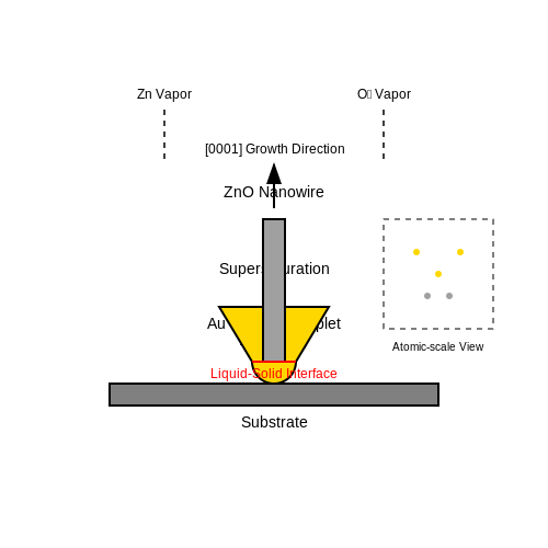
The VLS mechanism is the most widely used technique for synthesizing high-quality ZnO nanowires. A metal catalyst (typically Au) forms a liquid alloy with Zn at elevated temperatures, followed by supersaturation and nucleation at the liquid-solid interface. The growth direction is often along the [0001] c-axis due to the lowest surface energy.
- Temperature range: 850–950°C for optimal nanowire uniformity.
- Precursor: Zn vapor reacts with O2 to form ZnO.
- Catalyst size: Determines nanowire diameter (typically 20–100 nm).
Chemical Vapor Deposition (CVD) and Modifications
CVD-based techniques allow precise control over nanowire morphology. Plasma-enhanced CVD (PECVD) and metal-organic CVD (MOCVD) enable low-temperature growth (300–600°C), critical for flexible electronics. The reaction kinetics follow:
Hydrothermal and Solvothermal Synthesis
Solution-based methods offer scalability and low-cost fabrication. Hydrothermal growth involves aqueous precursors (e.g., Zn(NO3)2 and hexamethylenetetramine) at 60–120°C. Key parameters:
- pH: Affects nucleation density (optimal range: 10–12).
- Substrate pretreatment: Seed layers (e.g., ZnO nanoparticles) enhance vertical alignment.
Applications in Nanoelectronics
ZnO nanowires are integral to:
- Field-effect transistors (FETs): High electron mobility (~1000 cm²/V·s) in single-nanowire devices.
- Piezoelectric nanogenerators: Strain-induced polarization generates voltages up to 50 mV per wire.
- UV photodetectors: Responsivity > 10⁵ A/W due to large surface-to-volume ratio.
2.2 Nanorods and Vertical Alignment Methods
Structural Characteristics of ZnO Nanorods
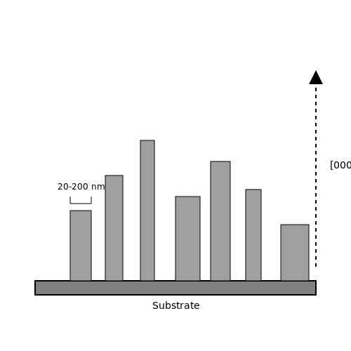
Zinc oxide (ZnO) nanorods exhibit a wurtzite crystal structure with a preferential c-axis orientation, resulting in anisotropic growth along the [0001] direction. The aspect ratio (length-to-diameter) typically ranges from 10:1 to 100:1, with diameters between 20–200 nm and lengths up to several micrometers. The high surface-to-volume ratio and defect-free single-crystalline nature make them ideal for charge transport applications.
Growth Mechanisms
Two primary methods dominate vertical alignment:
- Vapor-Liquid-Solid (VLS) Growth: Involves a metal catalyst (Au, Sn) forming a eutectic liquid droplet that directs one-dimensional growth. The process follows:
where L is nanorod length, Ω is atomic volume, J is vapor flux, and a is sticking coefficient.
- Hydrothermal Growth: Aqueous zinc nitrate/hexamine solutions facilitate low-temperature (70–95°C) growth. The reaction:
Alignment Control Parameters
Critical factors influencing vertical alignment include:
| Parameter | Effect | Optimal Range |
|---|---|---|
| Substrate Pretreatment | Seed layer crystallinity determines epitaxial matching | 5–50 nm ZnO seed layer |
| Growth Temperature | Higher temperatures enhance surface diffusion | 350–900°C (VLS), 70–95°C (hydrothermal) |
| Precursor Concentration | Controls nucleation density | 0.01–0.1 M (hydrothermal) |
Electrostatic Alignment Techniques
Post-growth alignment can be achieved via dielectrophoresis. The alignment torque τ on a nanorod in an AC field is:
where p is the induced dipole moment and E is the electric field. Optimal alignment occurs at frequencies where the Clausius-Mossotti factor peaks (typically 1–10 MHz).
Device Integration Challenges
Key considerations for electronic applications:
- Ohmic contact formation requires surface treatments (O2 plasma or NH3 annealing) to reduce Schottky barriers
- Inter-nanorod spacing must exceed Debye length (≈20 nm for doped ZnO) to prevent screening effects
- Mechanical stability demands Young's modulus matching (≈140 GPa for ZnO) with substrates
2.3 Quantum Dots and Colloidal Synthesis
Quantum Confinement in ZnO Nanostructures
The quantum confinement effect becomes significant when the physical dimensions of ZnO nanostructures approach the exciton Bohr radius (~2.34 nm for ZnO). This leads to discrete energy levels and size-tunable optical properties. The energy bandgap Eg of a quantum dot with diameter d follows:
where me* and mh* are the effective masses of electrons and holes respectively, and ϵr is the relative permittivity.
Colloidal Synthesis Methods
The most common approaches for producing ZnO quantum dots include:
- Sol-gel processing: Controlled hydrolysis of zinc precursors (e.g., zinc acetate) in alcoholic solutions
- Hot-injection: Rapid injection of precursors into high-temperature solvents (180-300°C) with surfactants
- Microemulsion: Water-in-oil systems with nanoscale reactors formed by surfactants
The growth kinetics follow the LaMer model, where burst nucleation occurs when precursor concentration exceeds critical supersaturation:
where N is the number density of nuclei, Cs is the saturation concentration, and n is the reaction order.
Surface Passivation and Stability
Unpassivated ZnO quantum dots suffer from surface defects acting as non-radiative recombination centers. Common passivation strategies include:
- Organic ligands (amines, thiols, carboxylic acids)
- Inorganic shells (ZnS, SiO2)
- Dual passivation using hybrid organic-inorganic approaches
The photoluminescence quantum yield (PLQY) improves dramatically with proper passivation, often exceeding 80% for core-shell structures. The radiative lifetime τr relates to the oscillator strength f through:
where VQD is the quantum dot volume and |ψ(0)|2 is the electron-hole wavefunction overlap.
Applications in Optoelectronics
ZnO quantum dots enable several advanced device applications:
- UV photodetectors: Exhibiting gain >105 due to high surface-to-volume ratio
- LED phosphors: Tunable emission from 370-550 nm via size control and doping
- Quantum dot solar cells: Achieving >8% efficiency in hybrid perovskite-ZnO architectures
Recent advances demonstrate electrically pumped lasing from ZnO quantum dot assemblies at threshold currents as low as 120 A/cm2, enabled by strong excitonic effects and high oscillator strengths.
2.4 Thin Films and Deposition Processes
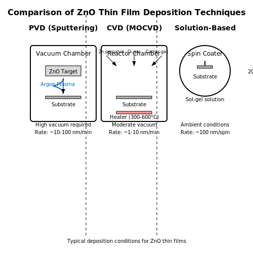
Zinc oxide (ZnO) thin films are integral to modern electronics due to their tunable optoelectronic properties, high electron mobility, and piezoelectric characteristics. The deposition process critically influences film morphology, crystallinity, and defect density, which in turn govern device performance. Key techniques include physical vapor deposition (PVD), chemical vapor deposition (CVD), and solution-based methods, each offering distinct advantages for specific applications.
Physical Vapor Deposition (PVD)
PVD techniques, such as sputtering and pulsed laser deposition (PLD), enable high-purity ZnO thin films with precise stoichiometric control. In magnetron sputtering, a plasma discharge ionizes argon gas, accelerating ions toward a ZnO target. The ejected atoms condense on a substrate, forming a thin film. The process is governed by:
where J is ion flux density, η is sputtering yield, M is molar mass, ρ is density, and NA is Avogadro’s number. Substrate temperature (Ts) and sputtering pressure (P) critically affect crystallinity, with optimal Ts typically between 200–400°C for (002)-oriented wurtzite structures.
Chemical Vapor Deposition (CVD)
CVD methods, including metal-organic CVD (MOCVD), utilize volatile precursors (e.g., diethylzinc and oxygen) that react on heated substrates. The growth kinetics follow:
where h is film thickness, k0 is a pre-exponential factor, Ea is activation energy, and Pprecursor is partial pressure. MOCVD excels in producing uniform, large-area films with controlled doping (e.g., Al:ZnO for transparent conductive oxides).
Solution-Based Deposition
Low-cost techniques like spin-coating and spray pyrolysis employ sol-gel precursors (e.g., zinc acetate in ethanol). The film formation involves hydrolysis and polycondensation reactions:
Post-annealing at 300–500°C removes organic residues and enhances crystallinity. While less precise than PVD/CVD, solution methods are scalable for flexible electronics and printed devices.
Characterization and Optimization
Critical parameters include:
- Thickness uniformity: Measured via ellipsometry or profilometry; deviations >5% degrade waveguide performance.
- Carrier concentration: Hall effect measurements reveal doping efficiency; optimal Al:ZnO films achieve ~1020 cm−3.
- Surface roughness: Atomic force microscopy (AFM) shows RMS values <2 nm for high-electron-mobility transistors (HEMTs).
Advanced methods like atomic layer deposition (ALD) achieve monolayer control, with growth rates of 0.1–0.2 nm/cycle, ideal for quantum well structures.
3. Transparent Conductive Electrodes
3.1 Transparent Conductive Electrodes
Zinc oxide (ZnO) nanostructures exhibit exceptional optoelectronic properties that make them ideal candidates for transparent conductive electrodes (TCEs). The wide bandgap (~3.3 eV) of ZnO enables high optical transparency in the visible spectrum, while doping with elements like aluminum (Al) or gallium (Ga) enhances electrical conductivity without significantly compromising transparency.
Charge Transport Mechanisms
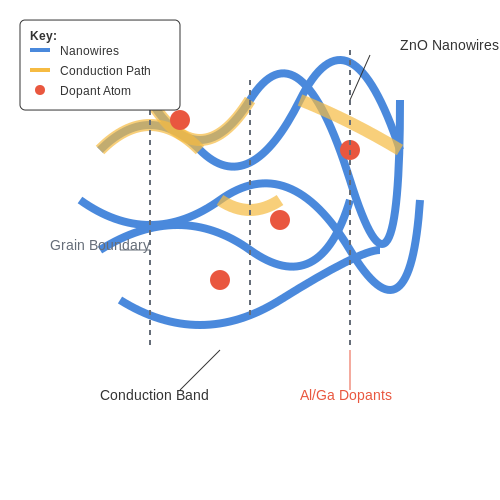
The electrical conductivity in doped ZnO nanostructures arises from two primary mechanisms:
- Ionized impurity scattering: Donor atoms (Al, Ga) introduce free electrons into the conduction band.
- Grain boundary scattering: Reduced in aligned nanowire arrays due to epitaxial growth.
where σ is conductivity, n is carrier concentration, e is electron charge, and μ is mobility.
Figure of Merit for TCEs
The Haacke figure of merit (ΦH) quantifies TCE performance:
where T is transmittance and Rs is sheet resistance. High-quality ZnO-based TCEs achieve ΦH > 10-2 Ω-1 with 85% transparency.
Nanostructure Optimization
Morphological control significantly impacts performance:
- Nanowire networks: Provide percolation pathways for charge transport
- Ultrathin films: (< 100 nm) maintain transparency while allowing carrier collection
- Hierarchical structures: Combine high surface area with continuous conduction paths
Fabrication Techniques
Advanced deposition methods enable precise control over ZnO TCE properties:
| Method | Advantages | Typical Rs (Ω/sq) |
|---|---|---|
| Sputtering | High uniformity, industrial scalability | 5-10 |
| ALD | Atomic-level thickness control | 15-30 |
| Electrospinning | Low-cost, flexible substrates | 50-100 |
Current Challenges
While ZnO TCEs show promise, several limitations remain:
- Environmental stability against humidity
- Contact resistance with organic semiconductors
- Thermal expansion mismatch with flexible substrates
3.2 UV Photodetectors and LEDs
Fundamental Principles of ZnO-Based UV Photodetectors
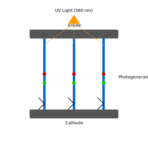
Zinc oxide (ZnO) nanostructures exhibit exceptional optoelectronic properties, making them highly suitable for ultraviolet (UV) photodetection. The wide bandgap (~3.37 eV at room temperature) allows ZnO to detect UV radiation while remaining transparent to visible light. The photodetection mechanism relies on electron-hole pair generation under UV illumination, where absorbed photons with energy exceeding the bandgap produce charge carriers that modify the material's conductivity.
The responsivity (R) of a ZnO-based UV photodetector is given by:
where Iph is the photocurrent and Popt is the incident optical power. The detectivity (D*), a measure of sensitivity, incorporates noise characteristics:
where A is the detector area, Δf is the bandwidth, and In is the noise current.
Nanostructure Engineering for Enhanced Performance
ZnO nanostructures—such as nanowires, nanorods, and quantum dots—offer high surface-to-volume ratios, improving light absorption and carrier collection efficiency. For instance, vertically aligned ZnO nanowires reduce carrier recombination by providing direct conduction pathways. Doping with elements like aluminum (Al) or gallium (Ga) further enhances conductivity and response speed.
The transient response time (τ) depends on carrier mobility (μ) and trap states:
where L is the interelectrode spacing and V is the applied bias. Reducing defect densities through annealing or surface passivation significantly improves response times.
ZnO in Light-Emitting Diodes (LEDs)
ZnO's high exciton binding energy (60 meV) enables efficient near-UV emission at ~380 nm. In heterostructure LEDs, ZnO is often paired with p-type materials (e.g., GaN or organic semiconductors) to form p-n junctions. The electroluminescence (EL) intensity follows:
where Ea is the activation energy for radiative recombination. Challenges include achieving stable p-type doping, which has been addressed using nitrogen (N) or phosphorus (P) dopants.
Practical Applications and Recent Advances
ZnO UV photodetectors are deployed in flame sensors, UV dosimetry, and missile plume detection. LEDs based on ZnO nanostructures are explored for solid-state lighting and optical communication. Recent studies demonstrate flexible ZnO photodetectors with graphene electrodes, achieving responsivities exceeding 105 A/W under low bias.
3.3 Piezoelectric Nanogenerators
Zinc oxide (ZnO) nanostructures exhibit strong piezoelectric properties due to their non-centrosymmetric wurtzite crystal structure. When subjected to mechanical strain, a polarization charge develops across the nanostructure, generating a potential difference. This effect forms the basis of piezoelectric nanogenerators (PENGs), which convert mechanical energy into electrical energy at the nanoscale.
Piezoelectric Effect in ZnO Nanostructures
The piezoelectric coefficient (d33) of ZnO nanowires typically ranges between 5–12 pm/V, significantly higher than bulk ZnO due to enhanced strain confinement in one-dimensional structures. The induced piezoelectric potential (Vpiezo) in a nanowire of length L and diameter D under axial strain ε is given by:
where σ is the applied stress, ϵr is the relative permittivity (~8.5 for ZnO), and ϵ0 is the vacuum permittivity. For a vertically aligned nanowire array, the total output voltage scales with the number of active nanowires in series.
Device Architectures
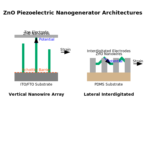
Two dominant PENG configurations exist:
- Vertical Nanowire Arrays: Grown on conductive substrates (e.g., ITO or FTO glass), with a top electrode that deforms under mechanical stress. The Schottky barrier at the metal-ZnO interface rectifies the AC piezoelectric output.
- Lateral Interdigitated Electrodes: Nanowires dispersed on flexible substrates (e.g., PDMS) between comb-shaped electrodes. Strain induces alternating potential gradients across the nanowire network.
Performance Optimization
Key parameters affecting PENG efficiency include:
where Y is Young’s modulus (~130 GPa for ZnO). Strategies to enhance performance:
- Doping: Aluminum or gallium doping increases carrier concentration, reducing internal impedance.
- Hybrid Structures: ZnO-PVDF composites combine high piezoelectric coefficients with mechanical flexibility.
- Surface Texturing: Hierarchical nanostructures (e.g., nanoflowers) amplify strain-induced charge separation.
Applications
ZnO-based PENGs have demonstrated:
- Energy harvesting from biomechanical motion (e.g., shoe-embedded generators producing 0.1–1 V/cm2 at 1 Hz).
- Self-powered sensors for pressure mapping (sensitivity ~28 mV/kPa).
- Implantable medical devices powered by cardiac motion (in vivo tests show 3 µW/cm2 output).
Recent advances include integrating PENGs with triboelectric layers to create hybrid nanogenerators, achieving power densities exceeding 10 W/m2 under impulsive loading.
3.4 Field-Effect Transistors (FETs)
Zinc Oxide as a Channel Material in FETs
Zinc oxide (ZnO) nanostructures exhibit exceptional electronic properties that make them highly suitable for field-effect transistors (FETs). The high electron mobility (μ ~ 200 cm²/V·s in bulk ZnO) and wide bandgap (~3.37 eV) enable low leakage currents and high breakdown voltages. When structured as nanowires or thin films, ZnO's surface-to-volume ratio enhances electrostatic gate control, improving the subthreshold swing (S) and on/off current ratio (Ion/Ioff).
The carrier concentration in ZnO FETs can be modulated by oxygen vacancies or intentional doping (e.g., Al, Ga). The conductance (G) follows:
where Cox is the gate oxide capacitance, W/L the aspect ratio, and Vth the threshold voltage. ZnO's piezoelectric properties further allow strain-gated transistors, where mechanical deformation modulates carrier mobility.
Device Architectures and Performance Metrics
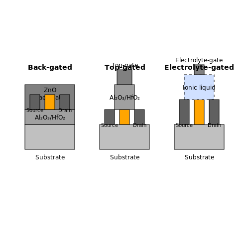
ZnO-based FETs are implemented in three primary configurations:
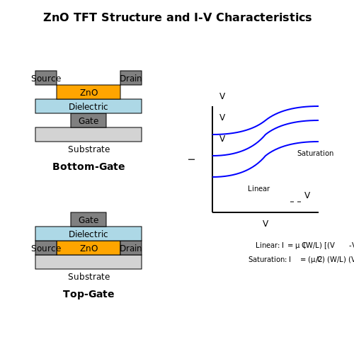
- Back-gated FETs: A global gate electrode beneath the substrate. Limited by high parasitic capacitance.
- Top-gated FETs: A localized gate dielectric (e.g., Al2O3, HfO2) deposited over the ZnO channel. Offers better electrostatic control.
- Electrolyte-gated FETs: Uses ionic liquids or gels as the gate medium, achieving high capacitance (~10 μF/cm²) at low voltages (<1 V).
Key performance parameters include:
- Threshold voltage (Vth): Ranges from −5 V to +5 V, tunable via doping or interface engineering.
- Subthreshold swing (S): Typically 80–200 mV/decade, approaching the Boltzmann limit (60 mV/decade) in optimized devices.
- On/off ratio: Exceeds 106 in nanowire FETs due to reduced defect density.
Fabrication Challenges and Solutions
ZnO FETs face challenges in stability and reproducibility:
- Oxygen vacancy migration: Causes threshold voltage drift. Solution: Passivation with SiO2 or PMMA.
- Contact resistance: Schottky barriers at metal-ZnO interfaces. Solution: Ohmic contacts using Ti/Au or Al/Ti stacks.
- Process variability: Nanowire alignment is critical. Solution: Dielectrophoresis or directed growth on patterned substrates.
Recent advances include hybrid structures, such as ZnO-graphene heterojunctions, which combine high mobility with mechanical flexibility.
Applications in Flexible and Transparent Electronics
ZnO FETs are integral to:
- Transparent displays: ZnO's wide bandgap enables >80% optical transparency in the visible spectrum.
- Wearable sensors: Piezoelectric ZnO nanowires detect strain, pressure, or biochemical signals.
- RF circuits: High-frequency operation (>1 GHz) is achievable due to low parasitic capacitance in nanostructures.
The following SVG illustrates a top-gated ZnO nanowire FET:
3.5 Gas and Chemical Sensors
Zinc oxide (ZnO) nanostructures exhibit exceptional sensitivity to gaseous and chemical species due to their high surface-to-volume ratio, tunable electronic properties, and strong surface reactivity. The sensing mechanism primarily relies on changes in electrical conductivity upon adsorption or desorption of target molecules, governed by surface charge transfer and oxygen vacancy interactions.
Surface Reaction Mechanisms
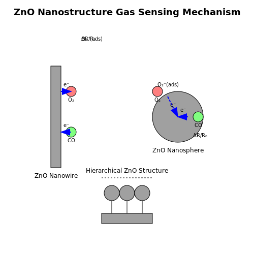
When ZnO nanostructures are exposed to oxidizing gases (e.g., O2, NO2), adsorbed oxygen species (O2−, O−) extract electrons from the conduction band, increasing resistance. For reducing gases (e.g., H2, CO), reactions release trapped electrons back into the conduction band, lowering resistance. The process is described by:
Key Performance Metrics
- Sensitivity (S): Defined as the ratio of resistance change (ΔR/R0) for resistive sensors or current/voltage shift for FET-based sensors.
- Response/Recovery Time: Governed by adsorption/desorption kinetics and diffusion rates.
- Selectivity: Enhanced through doping (e.g., Al, Ga) or surface functionalization.
Nanostructure Morphology Effects
Sensor performance is highly morphology-dependent:
- Nanowires: Fast response due to 1D electron transport but limited surface area.
- Porous Nanospheres: High sensitivity from increased gas adsorption sites but slower recovery.
- Hierarchical Structures (e.g., flower-like ZnO): Balance between surface area and charge transport.
Case Study: ZnO Nanorod FET Sensor for NH3 Detection
A field-effect transistor (FET) with ZnO nanorods as the channel material demonstrates sub-ppm NH3 detection. The gate voltage modulates carrier concentration, amplifying sensitivity. The drain current (ID) follows:
where μ is mobility, Cox is gate oxide capacitance, and Vth shifts upon NH3 adsorption.
Practical Challenges
- Humidity Interference: Competitive adsorption of H2O molecules necessitates hydrophobic coatings.
- Long-Term Stability: Surface passivation (e.g., SiO2 capping) mitigates oxidation degradation.
- Fabrication Scalability: Chemical vapor deposition (CVD) offers uniformity but at high cost.
Emerging Trends
Recent advances include plasmonic enhancement (Au/ZnO hybrids for LSPR-based optical sensing) and machine learning-assisted multi-analyte discrimination using impedance spectroscopy data.
4. Stability and Environmental Sensitivity
4.1 Stability and Environmental Sensitivity
Thermodynamic Stability of ZnO Nanostructures
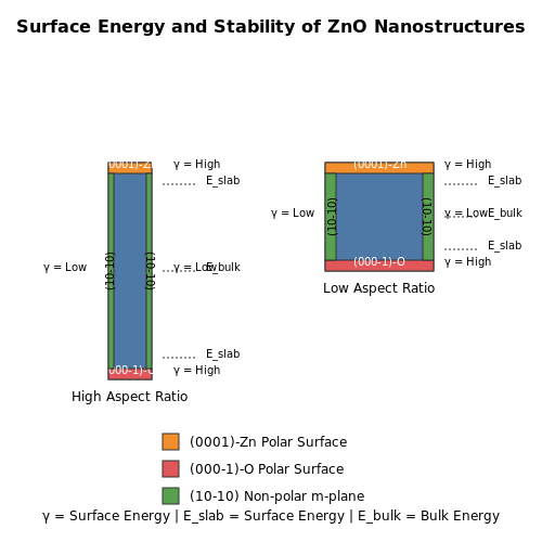
The stability of zinc oxide (ZnO) nanostructures is governed by their surface energy and thermodynamic equilibrium. The wurtzite crystal structure of ZnO exhibits polar surfaces, such as the (0001)-Zn and (000-1)-O terminated planes, which are inherently unstable due to uncompensated surface charges. The surface energy γ of a ZnO nanostructure can be expressed as:
where Eslab is the total energy of the nanostructure, N is the number of formula units, Ebulk is the energy per formula unit in the bulk crystal, and A is the surface area. Nanostructures with high aspect ratios, such as nanowires, exhibit increased stability due to the dominance of low-energy non-polar m-planes (10-10).
Environmental Sensitivity and Surface Reactions
ZnO nanostructures are highly sensitive to ambient conditions, particularly humidity and oxygen partial pressure. The adsorption of water molecules on ZnO surfaces leads to the formation of hydroxyl groups, which passivate surface states but also introduce additional scattering centers. The chemisorption process follows:
Under oxygen-rich environments, oxygen molecules adsorb onto zinc vacancies (VZn), forming acceptor-like surface states that significantly alter the electronic properties:
Degradation Mechanisms in Electronic Devices
In field-effect transistors (FETs) based on ZnO nanowires, environmental sensitivity manifests as threshold voltage shifts and mobility degradation. The time-dependent change in drain current ID follows stretched exponential kinetics:
where τ is the characteristic time constant and β is the dispersion parameter (typically 0.3–0.7 for ZnO). Encapsulation strategies using atomic layer deposition (ALD) of Al2O3 have proven effective, reducing degradation rates by up to two orders of magnitude.
Temperature-Dependent Behavior
The electrical conductivity σ of ZnO nanostructures follows Arrhenius behavior with two distinct regimes:
Below 150°C, the activation energy Ea corresponds to shallow donor ionization (30–60 meV), while above 150°C, it reflects oxygen vacancy migration (0.8–1.2 eV). This thermal sensitivity necessitates careful thermal management in power electronics applications.
Radiation Hardness
ZnO nanostructures exhibit remarkable radiation hardness compared to conventional semiconductors. Under gamma irradiation, the displacement damage coefficient Kd for ZnO nanowires is:
approximately three orders of magnitude lower than silicon. This property makes ZnO suitable for space electronics and nuclear environments.
4.2 Scalability and Cost-Effectiveness
Manufacturing Scalability of ZnO Nanostructures
The scalability of zinc oxide (ZnO) nanostructures hinges on their synthesis methods, which must balance high throughput with precise morphological control. Vapor-phase techniques like chemical vapor deposition (CVD) and pulsed laser deposition (PLD) achieve high crystallinity but suffer from limited batch processing capabilities. In contrast, solution-based methods such as hydrothermal synthesis offer superior scalability, with reaction volumes exceeding 100 liters in industrial settings. The governing equation for hydrothermal growth kinetics illustrates the trade-off between scalability and defect density:
where L is nanowire length, k0 the pre-exponential factor, and Ea the activation energy (typically 0.3–0.5 eV for ZnO). This Arrhenius-type relationship reveals why low-temperature hydrothermal methods (<100°C) dominate industrial production despite slightly lower mobilities (~50 cm2/V·s) compared to vapor-phase grown ZnO (~200 cm2/V·s).
Cost Analysis Across Synthesis Methods
A comparative cost breakdown for ZnO nanostructure production reveals stark differences:
- CVD: $$120–$$300 per gram (equipment + precursor costs)
- Hydrothermal: $$2–$$15 per gram (scales with V-0.7 for volume V)
- Electrodeposition: $$8–$$25 per gram (high purity variants)
The cost advantage of solution processing becomes pronounced when considering the yield-to-defect ratio (YDR), defined as:
Hydrothermal methods achieve YDR values >103, whereas vapor-phase techniques typically range from 101–102 due to stricter vacuum requirements.
Industrial Adoption Challenges
Despite cost advantages, three barriers hinder widespread ZnO adoption:
- Doping uniformity: Resistivity variations exceed ±15% in large-area hydrothermal films
- Contact engineering: Schottky barrier formation with common electrodes (Au, ITO)
- Pattern fidelity: Feature sizes >500 nm in solution-processed devices
Recent advances in aerosol jet printing have demonstrated 50 μm line resolutions with ZnO nanoparticulate inks, achieving sheet resistances of 104–105 Ω/sq at <$0.02/cm2. This approaches the cost structure of organic semiconductors while maintaining ZnO's environmental stability.
Case Study: Flexible Electronics Production
Roll-to-roll (R2R) manufacturing of ZnO nanowire arrays for flexible sensors exemplifies successful scaling. A 2023 pilot plant achieved 500 m2/day throughput with these parameters:
| Parameter | Value |
|---|---|
| Line speed | 2 m/min |
| Nanowire density | 108 cm-2 ± 12% |
| Power consumption | 0.8 kWh/m2 |
The process leverages continuous hydrothermal synthesis with in-line microwave annealing, reducing thermal budget by 60% compared to conventional furnaces. This demonstrates how integrated process engineering can overcome traditional scalability limits in oxide electronics.
4.3 Integration with Flexible Electronics
Mechanical Flexibility and Strain Tolerance
Zinc oxide (ZnO) nanostructures exhibit exceptional mechanical flexibility due to their high aspect ratio and crystalline anisotropy. The wurtzite crystal structure of ZnO allows for significant elastic deformation along the c-axis, with theoretical strain limits exceeding 5% before fracture. For a nanowire of length L and diameter d, the critical bending radius Rc before plastic deformation occurs is given by:
where E is Young's modulus (~130 GPa for ZnO) and σy is the yield strength (~2-3 GPa for nanostructures). This enables integration with polymer substrates like polyimide (PI) or polyethylene terephthalate (PET) that typically require bending radii >1 mm.
Hybrid Device Architectures
Three dominant integration approaches have emerged for flexible ZnO electronics:
- Direct growth on flexible substrates: Low-temperature hydrothermal synthesis (<150°C) enables ZnO nanowire growth on heat-sensitive polymers
- Transfer printing: Aligned nanowire arrays grown on rigid substrates can be transferred via PDMS stamping
- Nanocomposite embedding: ZnO nanoparticles dispersed in conductive polymer matrices (e.g., PEDOT:PSS)
Electrical Performance Under Deformation
The piezotronic effect in ZnO creates unique strain-dependent behavior. For a bent nanowire field-effect transistor (NWFET), the channel conductance G varies with applied strain ε:
where Πpiezo is the piezoresistive coefficient (~100-200 for ZnO), μ is carrier mobility, and ∂φSB/∂ε represents the strain-induced Schottky barrier modulation. This enables strain-gated transistors with sensitivity down to 0.01% strain.
Reliability Considerations
Cyclic bending tests reveal two primary failure modes:
- Nanowire-substrate delamination after >104 cycles at 1% strain
- Crack propagation at grain boundaries in polycrystalline ZnO films
Atomic layer deposition (ALD) of Al2O3 encapsulation layers has shown to improve cycling lifetime by 3-5x by preventing moisture ingress and mechanical wear.
Emerging Applications
Recent implementations demonstrate:
- Foldable active-matrix backplanes with ZnO TFTs (mobility >10 cm2/V·s at 2mm bending radius)
- Conformal pressure sensor arrays for robotic skin (sensitivity 28 kPa-1)
- Self-powered wearable sensors leveraging piezoelectric ZnO nanogenerators
4.4 Emerging Trends in ZnO-Based Devices
Flexible and Stretchable Electronics
Zinc oxide nanostructures are increasingly being integrated into flexible and stretchable electronic systems due to their mechanical robustness and piezoelectric properties. The wide bandgap (≈3.37 eV) and high exciton binding energy (60 meV) of ZnO make it suitable for flexible optoelectronics. Recent advances include:
- ZnO nanorod arrays embedded in polydimethylsiloxane (PDMS) for strain sensors with gauge factors exceeding 2000.
- Transparent conductive electrodes using Al-doped ZnO (AZO) nanowire networks with sheet resistances below 20 Ω/sq and >90% transparency.
where σ is conductivity, n is carrier concentration, e is electron charge, and μ is mobility. The high mobility (≈200 cm²/V·s) in ZnO nanowires enables superior flexible device performance.
Piezotronic Devices
The non-centrosymmetric wurtzite structure of ZnO generates piezoelectric potentials under mechanical stress, enabling novel piezotronic devices. Key developments include:
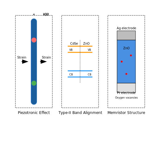
- Self-powered sensors utilizing the piezophototronic effect, where strain modulates carrier generation and separation at ZnO p-n junctions.
- Adaptive transistors with gate voltages generated internally by piezoelectric polarization charges.
The piezoelectric potential Vpz in a ZnO nanowire under strain ε is given by:
where e33 is the piezoelectric coefficient (1.22 C/m² for ZnO), κ is the dielectric constant, ε0 is vacuum permittivity, and L is the nanowire length.
UV Photodetectors with Gain Mechanisms
ZnO-based UV photodetectors now achieve ultrahigh gain through engineered nanostructures:
- Surface oxygen adsorption-desorption processes in ZnO nanowires create depletion layers that amplify photocurrent.
- Graphene-ZnO heterojunctions demonstrate gain >10⁸ due to charge trapping at interface states.
The photoconductive gain G is expressed as:
where τ is carrier lifetime, ttr is transit time, V is applied voltage, and L is interelectrode spacing.
Quantum Dot Hybrid Devices
Coupling ZnO with quantum dots (QDs) enables new functionalities:
- Type-II band alignment in CdSe/ZnO systems extends charge separation lifetimes to >100 ns.
- Solution-processed ZnO/QD LEDs achieve external quantum efficiencies exceeding 12%.
The Förster resonance energy transfer (FRET) efficiency E between QDs and ZnO is given by:
where R0 is the Förster radius and r is the QD-ZnO separation distance.
Neuromorphic Computing Elements
ZnO memristors are emerging as artificial synapses due to:
- Oxygen vacancy migration creating analog resistance states with >10⁶ endurance cycles.
- Spike-timing-dependent plasticity (STDP) demonstrated in Ag/ZnO/Pt devices with 100 ps switching.
The conductance update ΔG in a memristive synapse follows:
where A is a scaling factor, Δt is spike timing difference, and τ is the characteristic time constant.
5. Key Research Papers and Reviews
5.1 Key Research Papers and Reviews
- Rare Earth-Doped Zinc Oxide Nanostructures: A Review - ResearchGate — Rare Earth-Doped Zinc Oxide Nanostructures: A Review ... June 2016; Reviews in Nanoscience and Nanotechnology 5(1):1-27; ... teaching and research experience and has publis hed more than 500 ...
- PDF Zinc oxide nanostructures: growth, properties and applications — has the richest family of nanostructures among all materials, both in structures and in properties. The nanostructures could have novel applications in optoelectronics, sensors, transducers and biomedical sciences. This article reviews the various nanostructures of ZnO grown by the solid-vapour phase technique and their corresponding growth ...
- Nanostructured ZnO Materials: Synthesis, Properties and ... - Springer — Zinc oxide (ZnO) is an n-type semiconductor material with promising catalytic, electronic [], and optical properties.In the abovementioned fields, it possesses great potential because of its high electron mobility, high thermal conductivity, wide bandgap (∼3.3 eV) [], and large exciton-binding energy (∼60 meV) [] and exhibits UV absorption in the range 200-350 nm and emission in the near ...
- Electrochemical-Based Biosensors on Different Zinc Oxide Nanostructures ... — The focus of this paper is to comprehensively report on recent progress of ZnO electrochemical biosensors based on its dimensional classes. ... due to rich zinc and oxygen, and this surface electronic polarity phenomenon would affect ... Girija E.K. Morphology and size controlled synthesis of zinc oxide nanostructures and their optical ...
- Advances and significances of nanoparticles in semiconductor ... — This paper emphasizes the need for more research and development to get around current obstacles and guarantee their successful implementation while recognizing the promising role that nanoparticles will play in determining the future of semiconductor applications. ... Zinc oxide nanostructures with various shapes and structures have been ...
- Zinc oxide nanowires - ScienceDirect — This paper reviews some of the fundamental aspects of ZnO NW research and showcases the importance of ZnO NWs with proper properties for future applications. ... Rational synthesis of p-type zinc oxide nanowire arrays using simple chemical vapor deposition. ... Semiconducting and piezoelectric oxide nanostructures induced by polar surfaces. Adv ...
- Dielectric Properties of ZnO‐Based Nanocomposites and Their Potential ... — 5. Zinc Oxide (ZnO) Zinc oxide (ZnO) is an n-type semiconductor that belongs to the II-VI group of the periodic table. It has been extensively studied and analysed by numerous researchers due to its outstanding properties, which include cost-effectiveness, wide availability, and nontoxic nature [68 - 70]. ZnO exhibits a wide bandgap of 3.37 eV.
- Synthesis, Characterization, and Applications of ZnO Nanowires — They also play an important role as both interconnects and functional units in the fabrication of electronic, optoelectronic, electrochemical, and electromechanical nanodevices . Among the one-dimensional (1D) nanostructures, zinc oxide (ZnO) nanowire is one of the most important nanomaterials for nanotechnology in today's research .
- Study on structural, morphological, elastic and electrical properties ... — Zinc oxide (ZnO) nanoparticles have emerged as a versatile and compelling contender in the field of advanced materials for electronic device applications. Because of their unique physical and chemical properties, these materials prove exceptionally well-suited for diverse applications such as optoelectronics, acoustics, sensing, and laser ...
- Nanostructured ZnO Materials: Synthesis, Properties and Applications — SEM images of CVD-grown ZnO nanostructures: (a) nanorods with hexagonal cross section, (b) thin and large ribbons, (c) nanocombs, (d) tetrapods, (e) nanostructures mixed with tetrapods and powders ...
5.2 Books and Monographs on ZnO Nanostructures
- Zinc Oxide Materials for Electronic and Optoelectronic Device Applications — on the Energy of Optical Transitions in ZnO and GaN 51 2.8 Closely Spaced Donor-Acceptor Pairs in ZnO 55 2.9 Summary 58 References 58 3 Electrical Transport Properties in Zinc Oxide 61 B. Claflin and D. C. Look 3.1 Introduction 61 3.2 Hall-Effect Analysis 62 3.2.1 Single-Band Conduction 62 3.2.2 Two-Band Mixed Conduction 65
- PDF Metal oxide nanostructures / Vol. 5 / ZnO nanostructures and nanodevices — Zinc Oxide Nanostructures andTheir Nanodevice Applications Ahmad Umar, Yoon-Bong Hahn 1. Introduction 2 2. Crystal Structures and Lattice Parameters ofZnO 4 3. Synthetic MethodsofZinc OxideNanostructures 5 3.1. Vapor-Phase GrowthProcess 5 3.2. Solution-Phase GrowthProcess 7 4. Nanostructuresof ZnO: Growth andProperties 9 4.1. Nanorods and ...
- PDF A Review On Applications Of Zinc Oxide Nanostructures — Zinc oxide is a technologically important inorganic compound with the formula ZnO. Zinc and oxygen are the elements of group II and VI with atomic numbers 30 and 08 and atomic weights 65.382 and 15.999 respectively. In the stable form, zinc oxide takes a hexagonal wurtzite crystal structure with lattice parameters a = 3.2458Å and c = 5.2006Å (c/a
- One-dimensional ZnO nanostructures: fabrication, optoelectronic ... — One-dimensional (1D) zinc oxide (ZnO) nanostructures have been extensively and intensively studied for several decades not only for their extraordinary chemical and physical properties, but also for their current and future different electronic and optoelectronic device applications. This review provides a brief overview of the progress of different synthesis methods and applications of 1D-ZnO ...
- Optoelectronic and solar cell applications of ZnO nanostructures — ZnO has risen as a vital material for electron transportation in a greater number of solar cells based on nanostructures because of its abundance, nontoxicity, and high electron mobility. We performed first principle calculations on structural, optical, and electronic properties of 2D zinc oxide monolayer and bilayer honeycomb structures.
- Nanostructured ZnO Materials: Synthesis, Properties and ... - Springer — Zinc oxide (ZnO) is an n-type semiconductor material with promising catalytic, electronic [], and optical properties.In the abovementioned fields, it possesses great potential because of its high electron mobility, high thermal conductivity, wide bandgap (∼3.3 eV) [], and large exciton-binding energy (∼60 meV) [] and exhibits UV absorption in the range 200-350 nm and emission in the near ...
- Zinc Oxide: Fundamentals, Materials and Device Technology — 7 ZnO Nanostructures 7.1 Synthesis of ZnO Nanostructures 7.2 Applications of ZnO Nanostructures 8 Processing, Devices, and Heterostructures 8.1 A Primer to Semiconductor-Metal Contacts 8.2 Ohmic Contacts to ZnO 8.3 Schottky Contacts to ZnO 8.4 Etching of ZnO 8.5 Heterostructure Devices 8.6 Piezoelectric Devices 8.7 Sensors and Solar Cells Based ...
- PDF Zinc oxide nanostructures: growth, properties and applications — reviews the various nanostructures of ZnO grown by the solid-vapour phase technique and their corresponding growth mechanisms. The application of ZnO nanobelts as nanosensors, nanocantilevers, field effect transistors and nanoresonators is demonstrated. (Some figures in this article are in colour only in the electronic version) Contents 1.
- PDF Review of Zinc Oxide (Zno) Nanoparticles Applications and ... - Ijetcse — Zinc Oxide presents different physical and chemical properties which depends on the morphology of nanostructures, not only various synthesis methods but also the physical and chemical properties of synthesized zinc oxide are to be investigated in terms of its morphology [4]. Zinc Oxide (ZnO) is analyzed to
- ZnO nanostructures for optoelectronics: Material properties and device ... — ZnO nanostructures can be grown in a variety of morphologies and by a number of different methods. Fig. 1 shows some examples of various morphologies of ZnO nanostructures grown by vapor deposition, as well as solution-based growth. Some of the more exotic morphologies, such as tetrapod structures shown in Fig. 1 a and b, can be grown only in a small yield (several percents of the total number ...
5.3 Online Resources and Databases
- Zinc Oxide Materials for Electronic and ... - Wiley Online Library — Zinc oxide materials for electronic and optoelectronic device applications / edited by Cole W. Litton, Donald C. Reynolds, Thomas C. Collins. p. cm. — (Wiley series in materials for electronic & optoelectronic applications ; 35) Includes bibliographical references and index. ISBN 978--470-51971-4 (hardback) 1. Zinc oxide. 2.
- Nanostructured ZnO Materials: Synthesis, Properties and ... - Springer — Zinc oxide (ZnO) is an n-type semiconductor material with promising catalytic, electronic [], and optical properties.In the abovementioned fields, it possesses great potential because of its high electron mobility, high thermal conductivity, wide bandgap (∼3.3 eV) [], and large exciton-binding energy (∼60 meV) [] and exhibits UV absorption in the range 200-350 nm and emission in the near ...
- PDF DAVIS, KLINTON P., Ph.D. Sol-Gel Synthesis and Band Gap Engineering of ... — DAVIS, KLINTON P., Ph.D. Sol-Gel Synthesis and Band Gap Engineering of Zinc Oxide Nanostructures. (2021) Directed by Dr. Hemali Rathnayake. 104 pp. Zinc Oxide (ZnO) belongs to the (II-VI) wurtzite semiconductor that has found practical applications across multiple disciplines. One of its first main uses was in the
- Zinc oxide materials for electronic and optoelectronic device ... — Stanford Libraries' official online search tool for books, media, journals, databases, government documents and more. Zinc oxide materials for electronic and optoelectronic device applications [electronic resource] in SearchWorks catalog
- PDF Zinc oxide nanostructures: growth, properties and applications — has the richest family of nanostructures among all materials, both in structures and in properties. The nanostructures could have novel applications in optoelectronics, sensors, transducers and biomedical sciences. This article reviews the various nanostructures of ZnO grown by the solid-vapour phase technique and their corresponding growth ...
- PDF Fundamentals of zinc oxide as a semiconductor - University of Chicago — Rep. Prog. Phys. 72 (2009) 126501 A Janotti andCGVandeWalle A L Γ A H Γ-8-6-4-2 0 2 4 6 8 10 Energy (eV) K Zn O a c [0001] (a) (b) M Figure 1. The wurtzite crystal structure of ZnO with the lattice parameters a and c indicated in (a), and the calculated band structure of ZnO using the HSE hybrid functional in (b).The energy of the valence-band maximum (VBM) was set to zero.
- ZnO wide-bandgap semiconductor nanostructures: Growth, characterization ... — Abstract. This article describes the growth, characterization and applications of zinc oxide (ZnO) wide-bandgap semiconductor nanostructures. It first introduces the reader to the basic physics and materials science of ZnO, with particular emphasis on the crystalline structure, electronic structure, optical properties and materials properties of ZnO wide-bandgap semiconductors.
- Overview | ZnO Nanostructures: Fabrication and Applications | Books ... — Low dimensional functional nanomaterials remain a worldwide hot spot. They are ideal structural units for constructing functional nanodevices because of their special properties, and always lead to outstanding performance in multi-subject fields like energy, information, environment, microelectronics, biology, medicine, national defence, etc. Their family includes advanced carbon nanomaterials ...
- Three-Dimensional ZnO Hierarchical Nanostructures: Solution Phase ... — Zinc oxide (ZnO) nanostructures have been studied extensively in the past 20 years due to their novel electronic, photonic, mechanical and electrochemical properties. ... The above discussion shows that the hierarchical assembly in ZnO nanostructures is related to the electronic/optical properties and thus a wide range of potential applications ...
- ZnO nanostructures for optoelectronics: Material properties and device ... — ZnO nanostructures can be grown in a variety of morphologies and by a number of different methods. Fig. 1 shows some examples of various morphologies of ZnO nanostructures grown by vapor deposition, as well as solution-based growth. Some of the more exotic morphologies, such as tetrapod structures shown in Fig. 1 a and b, can be grown only in a small yield (several percents of the total number ...