Zinc Oxide Piezoelectric Devices
1. Crystal Structure and Piezoelectric Properties
Crystal Structure and Piezoelectric Properties
Hexagonal Wurtzite Structure
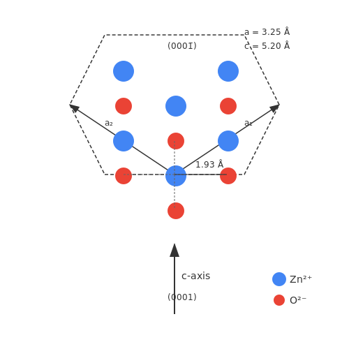
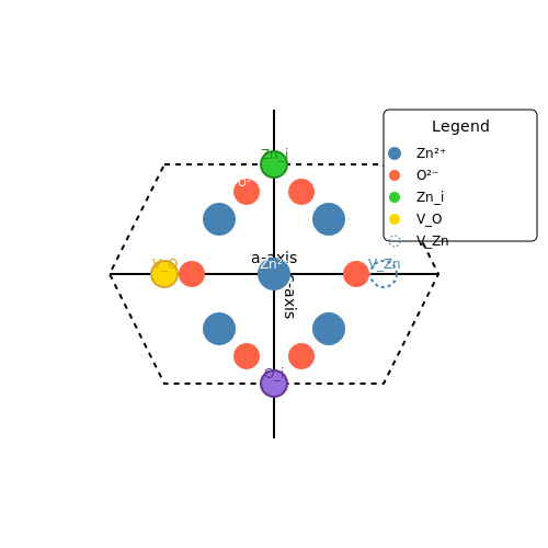
Zinc oxide (ZnO) crystallizes in the wurtzite structure, a hexagonal lattice system belonging to the P63mc space group. The unit cell consists of alternating layers of Zn2+ and O2- ions arranged in tetrahedral coordination. Each zinc atom is bonded to four oxygen atoms and vice versa, creating a non-centrosymmetric arrangement essential for piezoelectricity.
The lattice parameters are:
Piezoelectric Tensor and Polarity
The lack of inversion symmetry in ZnO’s wurtzite structure generates a spontaneous polarization along the c-axis ([0001] direction). The piezoelectric response is described by the third-rank tensor dijk, which reduces to two independent coefficients for hexagonal crystals:
where d33 represents the longitudinal effect (stress applied parallel to the c-axis), and d31 corresponds to the transverse effect (stress perpendicular to the c-axis).
Mathematical Derivation of Piezoelectric Coupling
The constitutive equations coupling mechanical strain (ε) and electric displacement (D) are:
where eijk is the piezoelectric stress tensor, κij is the dielectric permittivity, and Ej is the electric field. For ZnO, the simplified form along the polar axis is:
Practical Implications for Device Design
The strong piezoelectric coefficients and high electromechanical coupling factor (k33 ≈ 0.75) make ZnO ideal for:
- Ultrasonic transducers operating at frequencies > 1 GHz due to high sound velocity (~6,300 m/s).
- Flexural mode sensors leveraging d31 for in-plane strain detection.
- Energy harvesters where aligned c-axis films maximize charge output under mechanical stress.
Temperature and Doping Effects
Piezoelectric properties are temperature-dependent, with d33 decreasing by ~0.5%/°C above 300 K. Doping with elements like Al or Ga modifies conductivity while preserving piezoelectricity, enabling hybrid piezo-resistive devices.
1.2 Mechanism of Piezoelectric Response in ZnO
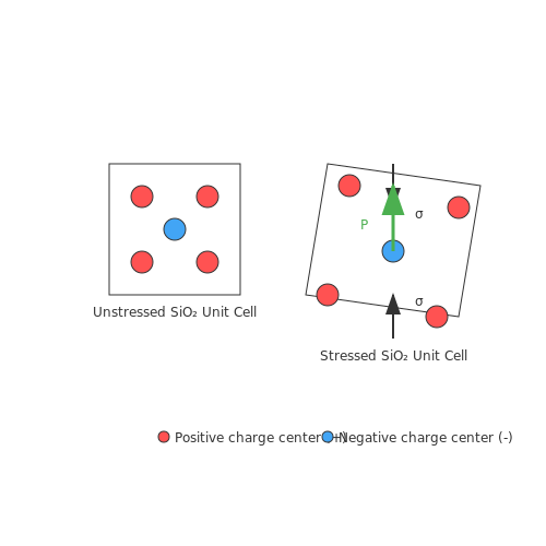
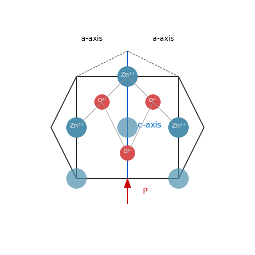
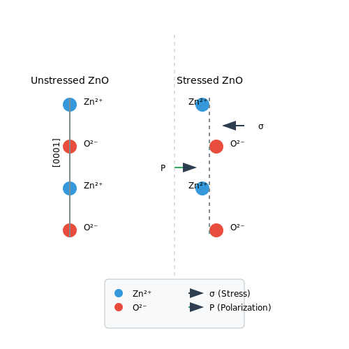
The piezoelectric effect in zinc oxide (ZnO) arises from its non-centrosymmetric wurtzite crystal structure (space group P63mc), where the Zn2+ and O2- ions occupy tetrahedral coordination sites. When mechanical stress is applied, the relative displacement of these sublattices generates a net dipole moment due to the asymmetric charge distribution.
Crystal Structure and Polarization
ZnO's wurtzite structure consists of alternating planes of Zn and O atoms stacked along the c-axis. The lack of inversion symmetry means that compressive or tensile strain along the polar [0001] direction produces a macroscopic polarization via the direct piezoelectric effect:
where Pi is the induced polarization vector, dijk is the third-rank piezoelectric tensor (with non-zero components d33, d31, and d15 for ZnO), and σjk is the applied stress tensor.
Mathematical Derivation of Piezoelectric Coefficients
The coupling between strain and polarization can be derived from the thermodynamic potential:
where cijkl are elastic stiffness coefficients, ϵij is strain, Ek is electric field, and ekij are piezoelectric stress constants. Minimizing Φ yields the constitutive relations:
Orientation-Dependent Response
The strongest piezoelectric response occurs along the c-axis due to the alignment of dipoles. For a ZnO thin film with c-axis orientation:
while the transverse coefficient d31 ≈ -5.0 pm/V. This anisotropy is exploited in devices like surface acoustic wave (SAW) filters where crystallographic cut determines performance.
Polarization Switching and Domain Dynamics
Unlike ferroelectric materials, ZnO exhibits non-switchable polarization. However, nanoscale studies reveal:
- Polarization reversal at high stresses (> 2 GPa) via oxygen vacancy migration
- Domain wall motion contributing to enhanced deff in polycrystalline films
- Flexoelectric effects becoming significant at sub-100 nm thicknesses
These phenomena are critical for designing high-frequency resonators and energy harvesters where strain gradients exceed 105 m-1.
1.3 Key Parameters Affecting Piezoelectric Performance
Piezoelectric Coupling Coefficient (k)
The electromechanical coupling coefficient k quantifies the efficiency of energy conversion between mechanical and electrical domains in zinc oxide (ZnO) devices. It is defined as:
For ZnO thin films, k typically ranges from 0.15 to 0.30, depending on crystal orientation and doping. The coupling coefficient directly impacts the bandwidth and sensitivity of piezoelectric transducers, with higher k values enabling more efficient energy harvesting applications.
Dielectric Constant (ε)
The relative permittivity of ZnO influences both electrical impedance matching and charge generation under mechanical stress. The dielectric constant varies with frequency due to domain wall motion and dipole relaxation effects:
where εs and ε∞ represent the static and high-frequency dielectric constants, respectively, and τ is the relaxation time. Optimizing ε requires balancing between high charge density (needed for sensors) and low dielectric loss (critical for resonators).
Mechanical Quality Factor (Qm)
Qm characterizes energy dissipation in the piezoelectric material and is defined as:
Single-crystal ZnO can achieve Qm > 10,000 at room temperature, while polycrystalline films typically exhibit Qm values between 500-2,000 due to grain boundary scattering. High Qm is essential for narrowband filters and timing applications.
Elastic Compliance (sE)
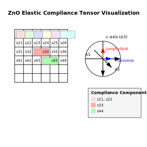
The compliance tensor sEij under constant electric field determines the mechanical deformation response to applied stress. For wurtzite ZnO (6mm symmetry), the reduced matrix form contains five independent components:
Epitaxial growth along the c-axis (002) orientation maximizes s33, enhancing longitudinal piezoelectric response for actuator applications.
Temperature Coefficients
The temperature dependence of key parameters follows:
- Piezoelectric coefficient (d33): -0.02% to -0.05%/°C due to thermal expansion mismatch
- Resonance frequency (fr): -50 to -80 ppm/°C governed by elastic stiffness variation
- Dielectric loss (tan δ): Increases exponentially above 150°C from ionic conduction
Aluminum doping (1-3 at.%) can reduce the temperature sensitivity of ZnO by stabilizing domain configurations.
Film Stress and Substrate Effects
Residual stress σ in sputtered ZnO films modifies piezoelectric performance through:
where Q12 is the electrostrictive coefficient. Compressive stress enhances d33 by 10-15% but reduces breakdown voltage. Silicon substrates induce tensile stress from thermal mismatch, while sapphire provides better lattice matching for low-stress films.
Electrode Materials and Interfaces
The work function difference between electrodes (Φ1 - Φ2) creates built-in potentials that affect polarization switching:
where Qint is the interface charge density. Platinum electrodes provide ohmic contacts with minimal interfacial reactions, while ITO enables transparent devices at the cost of higher series resistance.
2. Thin-Film Deposition Methods
2.1 Thin-Film Deposition Methods
Sputtering Techniques
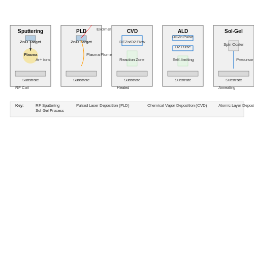
Radio-frequency (RF) magnetron sputtering dominates zinc oxide (ZnO) thin-film deposition due to its high deposition rates and excellent stoichiometric control. The process involves bombarding a ZnO target with argon ions in a vacuum chamber, typically at pressures between 1-10 mTorr. The sputtering yield Y follows:
where α is a material-dependent factor (0.15-0.25 for ZnO), M1 and M2 are masses of incident and target atoms, E0 is ion energy, and Us is surface binding energy (~7.8 eV for ZnO). Substrate heating between 200-400°C enhances c-axis orientation critical for piezoelectric response.
Pulsed Laser Deposition
PLD provides superior crystalline quality through ablation of a ZnO target with excimer lasers (KrF, 248 nm). The plasma plume dynamics obey the adiabatic expansion model:
where n is particle density, γ is the adiabatic index (5/3 for ZnO plasma), and cs is sound speed in the plume. Oxygen partial pressures of 10-100 mTorr and substrate temperatures of 600-800°C yield films with full-width-at-half-maximum (FWHM) rocking curves below 0.3°.
Chemical Vapor Deposition
Metalorganic CVD (MOCVD) using diethylzinc (DEZn) and oxygen precursors enables conformal coatings on complex geometries. The growth rate G follows Arrhenius behavior:
with activation energy Ea ≈ 1.2 eV and equilibrium constants KDEZn ≈ 10-3 Torr-1, KO2 ≈ 10-2 Torr-1. V/III ratios between 50-100 produce optimal piezoelectric coefficients d33 > 12 pm/V.
Atomic Layer Deposition
ALD achieves monolayer control through self-limiting surface reactions using alternating doses of DEZn and H2O. The growth per cycle (GPC) saturates at:
where θ represents surface coverage (typically 0.8-1.0 ML) and ρZnO is density (5.6 g/cm3). Temperatures of 150-200°C yield conformal films with roughness < 1 nm RMS, ideal for nanoscale devices.
Sol-Gel Processing
Solution-based methods employ zinc acetate precursors in alcoholic solvents, with hydrolysis reactions:
followed by polycondensation at 300-500°C. Multiple spin-coating iterations (5-10 layers) with 0.3-0.5 M concentrations produce films with e31,f coefficients up to -1.0 C/m2.
2.2 Nanostructure Synthesis Approaches
Vapor-Phase Growth Techniques
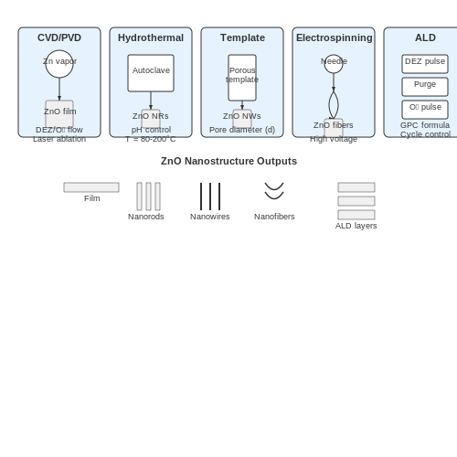
Vapor-phase deposition methods dominate high-quality zinc oxide (ZnO) nanostructure synthesis due to their precise control over crystallinity and stoichiometry. Chemical vapor deposition (CVD) and physical vapor deposition (PVD) are the most widely adopted. In CVD, precursor gases like diethylzinc (DEZ) and oxygen react at elevated temperatures (500–900°C) on a substrate, forming ZnO crystals. The reaction follows:
PVD techniques, such as pulsed laser deposition (PLD), ablate a ZnO target with a high-energy laser in a vacuum or oxygen-rich environment, yielding epitaxial films with minimal defects. The kinetic energy of ablated species (Ek) is critical for adhesion and crystallinity:
Solution-Based Methods
Wet-chemical approaches, including hydrothermal and solvothermal synthesis, offer scalable, low-cost alternatives. Hydrothermal growth involves aqueous zinc precursors (e.g., Zn(NO3)2) heated in autoclaves at 90–200°C, where pH and temperature dictate morphology. For instance, alkaline conditions (pH > 10) promote anisotropic growth into nanowires due to the preferential exposure of (002) crystal planes.
Solvothermal methods employ non-aqueous solvents (e.g., ethanol, ethylene glycol) to modulate reaction kinetics. Adding structure-directing agents like hexamethylenetetramine (HMTA) further controls aspect ratios, critical for piezoelectric response tuning.
Template-Assisted Synthesis
Porous templates (anodic aluminum oxide, polycarbonate membranes) enable precise diameter control of ZnO nanotubes or nanowires. Electrodeposition fills these templates with zinc ions, followed by thermal oxidation to ZnO. The pore diameter (d) and applied potential (V) govern growth rate (G):
where μe is electron mobility, z is charge number, F is Faraday’s constant, and ρ is density.
Electrospinning for Nanofibers
Electrospinning produces ultra-long ZnO-polymer composite fibers (50–500 nm diameter) for flexible piezoelectrics. A precursor solution (zinc acetate/polyvinylpyrrolidone) is ejected through a high-voltage needle, forming jets that solidify into fibers. Post-annealing at 400–600°C removes organics, leaving porous ZnO nanofibers with high surface-to-volume ratios.
Comparative Performance Metrics
The choice of synthesis method impacts key piezoelectric parameters:
- CVD/PVD: High crystallinity (d33 ≈ 10–12 pm/V) but limited scalability.
- Hydrothermal: Moderate performance (d33 ≈ 5–8 pm/V) with batch uniformity challenges.
- Electrospinning: Low cost, flexible substrates (d33 ≈ 3–6 pm/V), but lower charge mobility.
Emergent Techniques: Atomic Layer Deposition (ALD)
ALD achieves atomic-scale thickness control (< 1 nm) via self-limiting surface reactions. Sequential exposure to DEZ and H2O at 150–300°C yields conformal ZnO films ideal for MEMS applications. The growth per cycle (GPC) is given by:
where Δm is mass gain, A is substrate area, and N is cycle count.
2.3 Device Integration and Packaging
Mechanical and Electrical Interfacing
Zinc oxide (ZnO) piezoelectric devices require precise mechanical and electrical interfacing to ensure optimal performance. The piezoelectric coefficient (d33) governs the charge generation under mechanical stress, while the dielectric constant (εr) affects capacitive coupling. The generated voltage (V) can be expressed as:
where F is the applied force, t is the thickness, and A is the electrode area. Proper electrode alignment and stress distribution are critical to avoid depolarization or cracking.
Packaging Materials and Techniques
ZnO devices are sensitive to environmental factors such as humidity, temperature, and mechanical shock. Common packaging approaches include:
- Hermetic sealing with alumina or glass to prevent moisture ingress.
- Soft encapsulation using polydimethylsiloxane (PDMS) for flexible devices.
- Thermal management with heat sinks or thermally conductive adhesives for high-power applications.
Integration with CMOS and MEMS
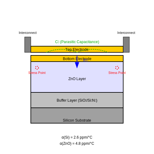
ZnO piezoelectric layers can be directly deposited on silicon substrates using sputtering or atomic layer deposition (ALD). Key challenges include:
- Thermal expansion mismatch between ZnO (α ≈ 4.5 × 10⁻⁶ K-1) and silicon (α ≈ 2.6 × 10⁻⁶ K-1).
- Parasitic capacitance from interconnect lines, which reduces the effective output voltage.
A common solution involves buffer layers of SiO2 or Si3N4 to mitigate stress.
Case Study: Energy Harvesting Module
A practical implementation for vibration energy harvesting integrates a ZnO nanowire array with a full-wave rectifier and charge pump. The power output (P) is given by:
where ω is the angular frequency, z0 is the displacement amplitude, and RL is the load resistance. Optimizing RL to match the device impedance maximizes power transfer.
Reliability and Testing
Accelerated lifetime testing involves:
- Thermal cycling (-40°C to 125°C) to assess interfacial delamination.
- Mechanical fatigue testing at resonant frequencies.
- Humidity exposure (85°C/85% RH) to evaluate corrosion resistance.
Failure modes include electrode oxidation, ZnO cracking, and delamination at the substrate interface.
3. Energy Harvesting Systems
3.1 Energy Harvesting Systems
Piezoelectric Energy Conversion Mechanism
The fundamental principle behind energy harvesting in zinc oxide (ZnO) piezoelectric devices lies in the direct piezoelectric effect, where mechanical strain induces an electric polarization. For a ZnO nanowire or thin film subjected to stress σ, the generated voltage V can be expressed as:
where g33 is the piezoelectric voltage coefficient (≈ 0.028 V·m/N for ZnO) and t is the thickness of the piezoelectric layer. The charge output Q follows:
with d33 being the piezoelectric charge coefficient (≈ 12.4 pC/N for ZnO) and F the applied force.
Device Architectures for Optimal Harvesting
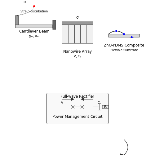
Three dominant configurations maximize energy conversion efficiency:
- Cantilever beams: Resonant structures with mass-loaded tips, optimal for low-frequency vibrations (10–200 Hz). Strain distribution follows:
where L is beam length, x is position, and δ is tip displacement.
- Vertical nanowire arrays: Compressive strain under axial loading, achieving power densities up to 80 µW/cm2 at 1 MPa stress.
- Flexible substrates: ZnO-polymer composites (e.g., PDMS) enable conformal deployment, with bending radii < 5 mm sustaining > 90% charge output.
Power Management Circuits
Impedance matching between the piezoelectric element (typically 10–100 kΩ) and storage circuitry is critical. A standard full-wave rectifier with smoothing capacitor yields:
where Vp is peak voltage, Cp is device capacitance, and RL is load resistance. Synchronous charge extraction (SCE) techniques improve efficiency to > 75% by actively switching storage capacitors at strain maxima.
Case Study: Footstep Energy Harvesting
A 5×5 cm2 ZnO nanowire array embedded in shoe insoles demonstrated:
- Peak voltage: 18 V per step (1.5 kN load)
- Energy per step: 2.3 mJ (0.46 mJ/cm2)
- Continuous power: 400 µW at 2 Hz walking frequency
This aligns with theoretical predictions from the modified Rayleigh-Lamb wave equation for contact mechanics:
where Em is Young's modulus, A is contact area, εmax is maximum strain, f is frequency, and κ is dielectric constant.
Advanced Materials Engineering
Doping strategies enhance performance:
- Al-doped ZnO: Increases d33 to 15.2 pC/N while reducing dielectric loss (tan δ < 0.02 at 1 kHz).
- Core-shell nanowires: ZnO/PVDF hybrids achieve 3X voltage output via strain confinement effects.
3.2 Sensors and Actuators
Piezoelectric Sensing Mechanism
The piezoelectric effect in zinc oxide (ZnO) arises from its non-centrosymmetric wurtzite crystal structure, which generates a charge separation under mechanical stress. The induced polarization P is proportional to the applied stress T through the piezoelectric coefficient tensor dij:
For ZnO thin films, the dominant coefficients are d33 (longitudinal) and d31 (transverse), typically ranging from 5-12 pC/N. The voltage output V across electrodes separated by thickness t is:
where F is the applied force, A the electrode area, and ϵr the relative permittivity (~8.5 for ZnO).
Actuation Principles
In actuator mode, an applied electric field E induces strain S through the converse piezoelectric effect:
ZnO actuators achieve displacements up to 0.1-0.3% of their length, with response times in the microsecond range. The blocking force Fb is constrained by Young's modulus Y (~210 GPa for ZnO):
Device Architectures
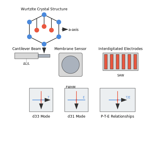
Common configurations include:
- Cantilever beams for accelerometers (sensitivity ~100 mV/g)
- Membrane structures for pressure sensors (range 0-100 kPa)
- Interdigitated electrodes for surface acoustic wave (SAW) devices
For ultrasonic transducers, the resonant frequency fr depends on the ZnO film thickness t and sound velocity v (~6330 m/s):
Fabrication Challenges
Key considerations for ZnO device fabrication include:
- Preferred c-axis orientation (XRD FWHM < 0.5° for optimal performance)
- Controlled oxygen vacancies (carrier concentration ~1017 cm-3)
- Stress management in thin films (typically 200-500 nm thickness)
Recent advances include textured ZnO nanowire arrays, which show 3-5× higher sensitivity compared to thin films due to enhanced strain confinement.
3.3 Biomedical Applications
Zinc oxide (ZnO) piezoelectric devices have gained significant traction in biomedical applications due to their biocompatibility, high electromechanical coupling, and ability to function in physiological environments. The following subsections detail key implementations.
Implantable Energy Harvesters
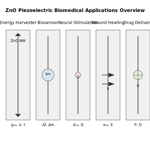
ZnO nanowire arrays are employed in self-powered implantable devices, converting biomechanical energy (e.g., blood flow, muscle contractions) into electrical energy. The generated voltage V follows:
where g33 is the piezoelectric voltage constant (≈ 0.03 V·m/N for ZnO), σ is applied stress, and t is thickness. For a 10 µm ZnO nanowire under 1 MPa stress:
Such harvesters power pacemakers at 5–20 µW/cm² without batteries.
Biosensors
ZnO’s high isoelectric point (≈ 9.5) enables immobilization of biomolecules. Piezoelectric biosensors detect mass changes via resonant frequency shift Δf:
where f0 is baseline frequency, Δm is adsorbed mass, A is electrode area, ρ is density, and μ is shear modulus. A 1 pg DNA attachment yields measurable shifts of 10–100 Hz at 200 MHz.
Neural Stimulation
ZnO microelectrodes deliver localized charge injections (< 1 nC/ph) for neuromodulation. The charge density Q is derived from the piezoelectric current I:
where d33 is the piezoelectric coefficient (12.4 pC/N for ZnO), F is force, and Rf, Cf are feedback components. This enables sub-µm precision in deep-brain stimulation.
Wound Healing
ZnO-polymer composites accelerate tissue regeneration by generating endogenous electric fields (50–200 mV/mm) under mechanical deformation. The field strength E correlates with strain ε:
where e33 is the piezoelectric stress constant (1.32 C/m² for ZnO), κ is dielectric constant (8.5), and ϵ0 is permittivity of free space. Clinical trials show 40% faster epithelialization at 100 mV/mm.
Drug Delivery
ZnO nanorod arrays release therapeutics upon ultrasonic excitation. The released dose D depends on acoustic pressure P and exposure time t:
where k is a material constant, Ea is activation energy (0.7 eV for ZnO-drug bonds), and kBT is thermal energy. Pulsatile insulin release achieves < 5% deviation from target glucose levels.
4. Enhancing Piezoelectric Coefficients
4.1 Enhancing Piezoelectric Coefficients
Fundamentals of Piezoelectric Response in ZnO
The piezoelectric coefficient (d33) in zinc oxide (ZnO) is governed by its wurtzite crystal structure, where non-centrosymmetric atomic arrangements enable charge separation under mechanical stress. The intrinsic piezoelectric response can be expressed as:
where Pz is the polarization along the c-axis and σz is the applied stress. For pure ZnO, d33 typically ranges from 9-12 pC/N, limited by ionic screening effects and crystal imperfections.
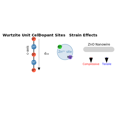
Doping Strategies for Enhanced Coefficients
Substitutional doping with transition metals (e.g., Co, Mn) or rare-earth elements (e.g., Eu, Er) modifies the ZnO lattice dynamics:
- Trivalent dopants (Al3+, Ga3+) increase charge carrier density while maintaining crystallinity, enhancing polarization response
- Divalent dopants (Mg2+, Cd2+) alter lattice parameters through ionic radius mismatch, creating localized strain fields
- Co-doping systems (e.g., Li+-Nb5+) introduce controlled defect dipoles that amplify piezoelectric coupling
where cdopant is dopant concentration and Δr/r0 is the relative ionic radius difference.
Microstructural Engineering Approaches
Controlled growth of ZnO nanostructures demonstrates significant enhancement effects:
| Morphology | d33 Enhancement | Mechanism |
|---|---|---|
| Vertically aligned nanowires | 2-3× bulk value | Strain confinement in 1D structures |
| Porous thin films | 1.5-2× dense films | Reduced dielectric stiffness |
| Textured polycrystals | 1.8× random orientation | C-axis alignment efficiency >85% |
Field-Assisted Poling Techniques
Post-synthesis electric field poling at elevated temperatures (150-300°C) aligns ferroelectric domains in doped ZnO:
where Ep is the poling field, μ is the domain dipole moment, and T is the poling temperature. Optimal conditions achieve >90% domain alignment with field strengths of 5-10 kV/cm.
Strain Engineering in Heterostructures
Epitaxial growth on lattice-mismatched substrates (e.g., sapphire, SiC) induces controlled strain:
Compressive strain along the a-axis enhances c-axis piezoelectric response through the Poisson effect. Recent work on ZnO/AlN superlattices demonstrates d33 values exceeding 25 pC/N due to interfacial strain coupling.
Practical Considerations for Device Integration
When implementing enhanced ZnO in devices:
- Thermal expansion mismatch with electrodes must be < 1.5 ppm/K to avoid delamination
- Doped ZnO requires oxygen-rich annealing (400-500°C) to maintain stoichiometry
- Nanostructured films need conformal electrode deposition (e.g., ALD-grown RuO2)
4.2 Stability and Reliability Issues
Mechanical Fatigue and Crack Propagation
Zinc oxide (ZnO) piezoelectric devices are subject to mechanical fatigue due to repeated stress cycles, particularly in high-frequency applications. The piezoelectric coefficient (d33) degrades over time as microcracks propagate along grain boundaries. The Paris-Erdogan law describes crack growth rate:
where da/dN is crack growth per cycle, ΔK is the stress intensity factor range, and C, m are material constants. For ZnO thin films, m typically ranges between 3–5 under cyclic loads exceeding 106 cycles.
Thermal Stability Limitations
ZnO’s piezoelectric performance deteriorates above 300°C due to oxygen vacancy migration and lattice distortion. The temperature-dependent polarization loss follows:
where Ea ≈ 0.5–1.2 eV for ZnO, and kB is Boltzmann’s constant. Devices operating in automotive or industrial environments require doping (e.g., Al, Ga) to suppress thermal depolarization.
Humidity-Induced Degradation
Hydroxyl (OH−) groups adsorb onto ZnO surfaces, forming non-piezoelectric Zn(OH)2 layers. The reaction kinetics obey:
where θ is surface coverage, k is the rate constant, and PH2O is water vapor pressure. Hermetic packaging (e.g., ALD Al2O3 barriers) reduces humidity sensitivity by 3–4 orders of magnitude.
Electrical Leakage and Breakdown
High electric fields (>100 kV/cm) induce ionic conduction through zinc interstitials (Zni2+), described by the Mott-Gurney law:
where μ is mobility, ε is permittivity, and d is film thickness. Breakdown occurs when leakage exceeds 10−6 A/cm2, necessitating Schottky contacts or bilayer dielectrics for suppression.
Accelerated Aging Tests
Industry-standard reliability assessments combine:
- Thermal cycling: −40°C to +125°C (JESD22-A104)
- Humidity exposure: 85°C/85% RH (JESD22-A101)
- Mechanical shock: 1500G, 0.5 ms (MIL-STD-883H)
Failure analysis typically reveals interfacial delamination as the dominant failure mode after 1000+ cycles.
Mitigation Strategies
Recent advances improve stability through:
- Nanocomposites: ZnO-carbon nanotube hybrids reduce crack propagation by 60%
- Graded doping: Ti/Zr concentration gradients enhance thermal stability up to 400°C
- Topological electrodes: Fractal-shaped interdigitated electrodes minimize field crowding
4.3 Scalability and Cost Considerations
Material Synthesis and Fabrication Costs
The scalability of zinc oxide (ZnO) piezoelectric devices is heavily influenced by the cost of material synthesis and device fabrication. ZnO is advantageous compared to lead-based piezoelectrics (e.g., PZT) due to its lower raw material costs and compatibility with large-scale deposition techniques. The primary methods for ZnO thin-film synthesis include:
- Sputtering: High-quality films are achievable, but equipment costs and deposition rates impact scalability.
- Chemical Vapor Deposition (CVD): Offers uniformity over large areas but requires precise control of precursor gases.
- Sol-Gel Processing: Low-cost and scalable for coatings, though film quality may vary.
The cost per unit area C can be approximated by:
where Cmaterial is the raw material cost, Cprocess includes energy and labor, and Cequipment is amortized over N production units.
Device Integration and Manufacturing Challenges
ZnO devices must integrate with existing semiconductor or flexible electronics manufacturing lines to minimize retrofitting costs. Key challenges include:
- Thermal Budget: ZnO deposition often requires temperatures above 300°C, incompatible with some polymer substrates.
- Patternability: Etching ZnO without damaging underlying layers adds complexity.
- Yield: Defect density scales with device area, affecting large-scale production.
For MEMS-scale devices, the yield Y follows the Poisson model:
where D is defect density (cm−2) and A is device area (cm2).
Comparative Cost Analysis
ZnO competes with other piezoelectrics in cost-sensitive applications. A breakdown for 1 cm2 devices:
| Material | Raw Cost ($$/cm2) | Processing Cost ($$/cm2) |
|---|---|---|
| ZnO (sputtered) | 0.05–0.15 | 0.20–0.50 |
| PZT | 0.30–0.60 | 0.80–1.50 |
| AlN | 0.10–0.25 | 0.40–0.90 |
ZnO’s cost advantage diminishes for high-performance applications requiring AlN’s superior thermal stability.
Scalability in Flexible Electronics
Roll-to-roll (R2R) processing enables low-cost ZnO piezoelectric arrays for energy harvesting. Critical parameters include:
- Substrate Compatibility: Polyimide or PEN films limit processing temperatures to <200°C.
- Throughput: R2R sputtering achieves ~10 m/min, but crystallinity suffers at high speeds.
The trade-off between throughput v and piezoelectric coefficient d33 follows:
where k is a process-dependent constant.
Case Study: Large-Area Pressure Sensors
A 2022 pilot line for ZnO-based pressure sensors achieved $$0.12/cm2 at 10,000-unit batches, compared to $$0.08/cm2 projected for 1M units. The cost reduction primarily came from:
- 30% lower waste via improved shadow masking.
- 15% faster deposition using pulsed DC sputtering.
- Reuse of carrier substrates in batch processing.
5. Key Research Papers on ZnO Piezoelectricity
5.1 Key Research Papers on ZnO Piezoelectricity
- ZnO Piezoelectric Devices - ScienceDirect — This chapter focuses on the progress of piezoelectric zinc oxide (ZnO) and its device applications. Piezoelectricity is the mechanism of converting mechanical energy into electrical energy and vice versa. ... The conclusion and outline of future research work can be found in Section 13.6. 13.2 Piezoelectric properties of ZnO Piezoelectricity is ...
- A review on ZnO-based piezoelectric nanogenerators: Synthesis ... — The common precursors used for the growth of ZnO NRs are zinc powder and zinc oxide powder. A trace amount of oxygen gas is normally required. The typical synthesis temperature is in the range of 450-900 °C for zinc powder [51, 52] and up to 1200 °C when zinc oxide power [53] is used to generate the vapour phase of zinc. The zinc vapour is ...
- Piezoelectric properties of ZnO - ScienceDirect — Zinc oxide (ZnO) is an exceptional material that displays multiple semiconducting, piezoelectric, and pyroelectric properties. ... advanced powering sources are to a great extent vital for maintenance-free and sustainable control of the electronic devices. ... Zinc -oxide piezoelectric nano-generators for low frequency applications. Semicond ...
- Design of a piezoelectric energy harvesting device based on ZnO ... — Nowadays, the development of renewable energy receives much attention as demand to sustain energy and reduce fossil fuels emissions grows. Accordingly, numerous piezoelectric materials and applications were developed [1-4].Among all the known piezoelectric harvesters, zinc oxide (ZnO) has become one of the most promising pioneers in the energy harvesting field.
- Controlled Growth of Semiconducting ZnO Nanorods for Piezoelectric ... — Zinc oxide (ZnO) nanorods have attracted considerable attention in recent years owing to their piezoelectric properties and potential applications in energy harvesting, sensing, and nanogenerators. Piezoelectric energy harvesting-based nanogenerators have emerged as promising new devices capable of converting mechanical energy into electric energy via nanoscale characterizations such as ...
- PDF Fabrication of Zinc Oxide Piezoelectric Nanostructures: A route ... - UP — and higher conversion rate when compared to bulk. The zinc oxide (ZnO) is a crystal with wurtzite structure, thus having piezoelectric properties. In this work one was able to produce and characterize different ZnO nanostructures (thin films, nanowires and nanoparticles) and successfully apply the nanowires to produce a novel piezoelectric
- Doped Zinc Oxide‐Based Piezoelectric Devices for Energy Harvesting and ... — In scholarly research, attention has predominantly been given to either exploring the piezoelectric characteristics (e.g., the d 33 value) and other enhanced features of doped ZnO or to the creation of PENG-based devices like EHs and sensors using specific element-doped ZnO. Yet, a comprehensive review comparing all types of doped ZnO for PENG device development is lacking.
- PDF Utilization of Piezoelectric Effect in Zinc Oxide Nanowires As a ... — initiated [1]. Among materials for clean energy, Zinc Oxide (ZnO) holds a special stature due to its phenomenal properties. ZnO can be synthesized by many facile methods including hydrothermal, co-precipitation, sol-gel, and lots of other methods, and its morphology can be controlled easily by selecting the optimum synthesis method.
- PDF Zinc Oxide Piezoelectric Nanogenerators - library.nexteinstein.org — In this project the fabrication of piezoelectric nanogenerators, based on Zinc Oxide nanowires, is discussed. Zinc oxide nanowires exhibit inherent piezoelectric behaviour. It thus generates electricity when the nanowires are bent or a strain is applied. The aqueous solution method was chosen for the
- Towards a Highly Efficient ZnO Based Nanogenerator — 2. Piezoelectric Nanogenerator (PENGs) In 1880, Pierre and Jacques Curie realized the presence of the piezoelectric effect, which occurs in bulk or nanostructured semiconductor crystals, where the central symmetry is broken under the action of an external force, and thus produces the potential for a piezoelectric generation [].The PENG is one of the most promising portable energy-harvester ...
5.2 Books and Review Articles
- A review on ZnO-based piezoelectric nanogenerators: Synthesis ... — The performance of ZnO NRs based piezoelectric devices such as piezoelectric gated diodes [30], field-effect transistors [31, 32], ... [51, 52] and up to 1200 °C when zinc oxide power [53] is used to generate the vapour phase of zinc. The zinc vapour is adsorbed on the surface of the heated substrate and is reacted with oxygen for the growth ...
- A Systematic Review of Piezoelectric Materials and Energy Harvesters ... — Briscoe J., Dunn S. Piezoelectric Nanogenerators—A Review of Nanostructured Piezoelectric Energy Harvesters. 1st ed. Volume 14. Springer International Publishing; Cham, Switzerland: 2014. Piezoelectricity and Ferroelectricity; pp. 15-29. [Google Scholar] 29. Chopra I. Review of State of Art of Smart Structures and Integrated Systems.
- ZnO Piezoelectric Devices - ScienceDirect — This chapter focuses on the progress of piezoelectric zinc oxide (ZnO) and its device applications. Piezoelectricity is the mechanism of converting mechanical energy into electrical energy and vice versa. ... 13.3.4 Growth of piezoelectric MgxZn1-xO films Magnesium zinc oxide (MgxZn1-xO) is a new piezoelectric material formed by alloying ZnO ...
- Review on ZnO-based piezotronics and piezoelectric nanogenerators ... — Piezoelectric effects exist in both natural, including quartz, Rochelle salt, and topaz, and man-made piezoelectric materials, such as barium titanate (BaTiO 3) and lead zirconate titanate (Pb(Zr x Ti 1−x)O 3) (referred to as PZT) etc. Due to the growing environmental concerns of toxicity in lead-containing devices and demanding for developing multifunctional devices, there has been a push ...
- PDF Fabrication of Zinc Oxide Piezoelectric Nanostructures: A route ... - UP — and higher conversion rate when compared to bulk. The zinc oxide (ZnO) is a crystal with wurtzite structure, thus having piezoelectric properties. In this work one was able to produce and characterize different ZnO nanostructures (thin films, nanowires and nanoparticles) and successfully apply the nanowires to produce a novel piezoelectric
- Piezoelectric Nanomaterials for Energy Harvesting — 5.2.1 Zinc Oxide. Zinc oxide (ZnO) is a piezoelectric and semiconducting material that has been central to recent developments in nanoscale energy harvesting research. ZnO exists as 3 distinct crystal structures, namely wurtzite, zinc blende (sphalerite), and rock salt .
- Doped Zinc Oxide‐Based Piezoelectric Devices for Energy Harvesting and ... — In scholarly research, attention has predominantly been given to either exploring the piezoelectric characteristics (e.g., the d 33 value) and other enhanced features of doped ZnO or to the creation of PENG-based devices like EHs and sensors using specific element-doped ZnO. Yet, a comprehensive review comparing all types of doped ZnO for PENG device development is lacking.
- Piezoelectric Materials for Energy Harvesting and Sensing Applications ... — Examples of hybrid fillers include NaNbO 3-reduced graphene oxide (rGO), titanium oxide (TiO 2)-rGO nanotubes, manganese oxide (MnO 2)/graphene/MWCNT hybrid, etc. In this section, we will perform an in-depth review of piezoelectric properties of nanocomposites synthesized using the fillers mentioned above in PVDF and PDMS-based polymer matrix.
- Physics-Based Device Models and Progress Review for Active ... — where F is the applied force and A is the cross-sectional area. Consequently, the piezoelectric coefficient d 33 determines the material's electronic response to stress. While PZT possesses a strong d 33 component of 374 pC/N [], piezoelectric semiconductors such as ZnO and GaN have relatively low d 33 coefficients of 12.4 pC/N and 3.1 pC/N, respectively [19,20].
- PDF Zinc Oxide Piezoelectric Nanogenerators - library.nexteinstein.org — Piezoelectric nanogenerators appear to be a very promising option, with a range of applications in self-powered technology, where electricity can be produced without the need for a battery supply. In this project the fabrication of piezoelectric nanogenerators, based on Zinc Oxide nanowires, is discussed.
5.3 Online Resources and Datasets
- Piezoelectric Properties of Zinc Oxide Thin ... - Wiley Online Library — 1 Introduction. Zinc oxide (ZnO) has attracted a lot of interest in material research due to its wide bandgap energy (3.37 eV), [] high excitonic binding energy (60 mV), [] and relatively high piezoelectric coefficients (d 33 = 11.67 pC N −1 and d 31 = −5.43 pC N −1, for bulk ZnO). [] Such properties, associated with its wurtzite structure, make ZnO of particular interest in many ...
- Review of Zinc Oxide Piezoelectric Nanogenerators: Piezoelectric ... — Lead-free piezoelectric materials, such as barium titanate (BaTiO 3), zinc oxide, and polyvinylidene fluoride (PVDF), are currently being developed for use in piezoelectric energy harvesters [4,6,8,9,10,11]. In bulk form, the piezoelectric properties of lead-free piezoelectric materials are significantly lower and can be an order of magnitude ...
- Doped Zinc Oxide‐Based Piezoelectric Devices for Energy Harvesting and ... — In scholarly research, attention has predominantly been given to either exploring the piezoelectric characteristics (e.g., the d 33 value) and other enhanced features of doped ZnO or to the creation of PENG-based devices like EHs and sensors using specific element-doped ZnO. Yet, a comprehensive review comparing all types of doped ZnO for PENG device development is lacking.
- Modelling and Simulation of a Vertically Integrated Zinc Oxide ... — In this paper, a vertically integrated single piezoelectric Zinc Oxide nanowire-based system is modelled for energy harvesting applications. To reinforce this development, different structures of nanogenerators were modelled and simulated using COMSOL Multiphysics 5.3 software for their performance upgrades. ... Electronic ISBN: 978-1-6654-8786 ...
- Piezoelectric properties of ZnO - ScienceDirect — Zinc oxide (ZnO) is an exceptional material that displays multiple semiconducting, piezoelectric, and pyroelectric properties. ... advanced powering sources are to a great extent vital for maintenance-free and sustainable control of the electronic devices. ... Zinc -oxide piezoelectric nano-generators for low frequency applications. Semicond ...
- Restoring Piezoelectric Properties in 2D Zinc Oxide Nanosheets by ... — Nanoelectronic devices that are self-powered through the conversion of mechanical energy into electronic energy are of great interest for the fields of wearables and medical implants. The ability to find nanomaterials that have piezoelectric properties suitable for nanogenerators can be a challenge. Zinc oxide (ZnO) is a well-known material that has one of the highest piezoelectric tensors ...
- ZnO Piezoelectric Devices - ScienceDirect — This chapter focuses on the progress of piezoelectric zinc oxide (ZnO) and its device applications. Piezoelectricity is the mechanism of converting mechanical energy into electrical energy and vice versa. The generation of electrical polarization when a piezoelectric material is strained is known as the direct piezoelectric effect.
- PDF Zinc Oxide Piezoelectric Nanogenerators - library.nexteinstein.org — In this project the fabrication of piezoelectric nanogenerators, based on Zinc Oxide nanowires, is discussed. Zinc oxide nanowires exhibit inherent piezoelectric behaviour. It thus generates electricity when the nanowires are bent or a strain is applied. The aqueous solution method was chosen for the
- Area-Selective Growth of Zinc Oxide Nanowire Arrays for Piezoelectric ... — 1. Introduction. Piezoelectric energy harvesting is a renewable-energy-harvesting technology that refers to the capturing of energy from mechanical vibration and converting it into electrical energy to power nano- and micro-scale devices that do not have access to an external power supply [].Here, piezoelectricity is used as the natural property of certain materials to generate electric ...