Zinc Oxide UV Photodetectors
1. Basic Principles of UV Photodetection
Basic Principles of UV Photodetection
Fundamental Mechanism
UV photodetection relies on the photoelectric effect, where incident photons with energy greater than the bandgap of the detecting material generate electron-hole pairs. For zinc oxide (ZnO), which has a direct bandgap of approximately 3.37 eV, this corresponds to a cutoff wavelength of around 368 nm, placing it firmly in the ultraviolet spectrum. The generated carriers are then collected as photocurrent, which is proportional to the incident optical power.
Key Performance Parameters
The performance of UV photodetectors is characterized by several critical parameters:
- Responsivity (R): The ratio of photocurrent to incident optical power, typically expressed in A/W.
- Quantum Efficiency (η): The number of electron-hole pairs generated per incident photon.
- Detectivity (D*): A measure of the detector's ability to detect weak signals, accounting for noise.
- Response Time: The speed at which the detector responds to changes in illumination.
Noise Sources and Signal-to-Noise Ratio
The primary noise sources in UV photodetectors include shot noise, thermal noise, and 1/f noise. The signal-to-noise ratio (SNR) is crucial for determining the minimum detectable power. For a ZnO-based detector, the SNR can be expressed as:
Device Architectures
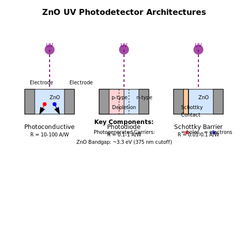
ZnO UV photodetectors can be implemented in various configurations, each with distinct advantages:
- Photoconductive Detectors: Rely on changes in conductivity due to photogenerated carriers.
- Photodiode Detectors: Operate in photovoltaic or reverse-biased modes for faster response.
- Schottky Barrier Detectors: Utilize metal-semiconductor junctions for high sensitivity.
Material Considerations
The performance of ZnO photodetectors is influenced by material properties such as crystallinity, defect density, and doping. High-quality ZnO films with low defect concentrations exhibit lower dark currents and higher responsivities. Doping with elements like aluminum or gallium can enhance conductivity and tailor the spectral response.
Practical Applications
ZnO UV photodetectors are employed in diverse applications, including flame detection, UV astronomy, and biological sensing. Their robustness, chemical stability, and tunable optoelectronic properties make them ideal for harsh environments where conventional silicon-based detectors may fail.
Unique Properties of Zinc Oxide for UV Detection
Wide Bandgap for UV Selectivity
Zinc oxide (ZnO) possesses a direct bandgap of approximately 3.37 eV at room temperature, corresponding to an absorption edge near 368 nm. This places ZnO firmly in the UV-A (320–400 nm) and UV-B (280–320 nm) detection range while remaining transparent to visible light. The wide bandgap minimizes interference from visible photons, enabling high spectral selectivity—a critical advantage over silicon-based detectors that require additional optical filters.
High Exciton Binding Energy
With an exciton binding energy of 60 meV (compared to 25 meV for GaN), ZnO exhibits strong excitonic effects at room temperature. This enhances UV absorption efficiency through exciton-related transitions rather than band-to-band transitions alone. The high binding energy also reduces thermal dissociation of excitons, improving detector responsivity.
Radiation Hardness and Thermal Stability
ZnO demonstrates exceptional stability under high-energy UV radiation due to its strong ionic bonding (Zn-O bond energy ~5.8 eV). Unlike organic photodetectors, ZnO maintains performance after prolonged UV exposure, with studies showing less than 5% responsivity degradation after 1000 hours at 10 mW/cm2 UV intensity. Its thermal conductivity (~50 W/m·K) further enables operation at elevated temperatures up to 400°C.
Native Defects and Doping Versatility
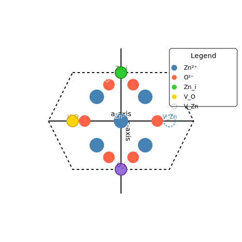
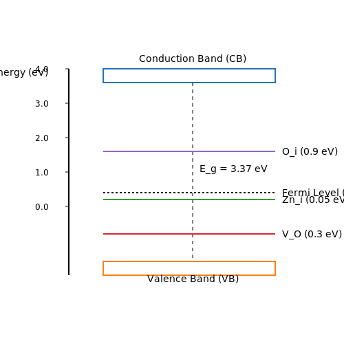
Native point defects in ZnO—particularly oxygen vacancies (VO) and zinc interstitials (Zni)—create n-type conductivity without intentional doping. Controlled introduction of these defects allows tuning of carrier concentration from 1015 to 1019 cm-3. For p-type operation, nitrogen or phosphorus doping can be employed, though with lower hole mobility (~10 cm2/V·s).
Defect-Related Energy Levels
- VO introduces a donor level ~0.3 eV below conduction band
- Zni acts as a shallow donor (~0.05 eV)
- Oxygen interstitials (Oi) form deep acceptors at ~0.9 eV above valence band
Piezoelectric and Pyroelectric Effects
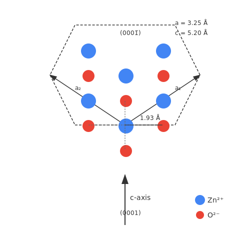
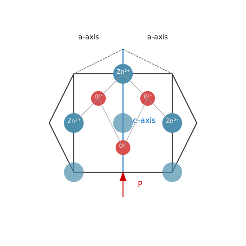
The wurtzite crystal structure of ZnO generates spontaneous polarization along the c-axis, enabling dual-mode UV detection:
- Piezophototronic effect: Strain-induced piezoelectric potential modulates Schottky barrier height at metal-ZnO contacts, enhancing photocurrent gain by up to 103.
- Pyroelectric detection: Temperature fluctuations from UV absorption produce transient currents, useful for pulsed UV monitoring.
Solution Processability
ZnO nanostructures can be synthesized through low-cost solution methods (e.g., hydrothermal growth at <100°C), enabling deposition on flexible substrates. Nanowire arrays grown via this method achieve aspect ratios >100:1, providing large surface-to-volume ratios for enhanced UV absorption while maintaining transparency in the visible spectrum.
Quantum Efficiency Comparison
| Material | External Quantum Efficiency (300 nm) | Dark Current Density (A/cm2) |
|---|---|---|
| ZnO | 65–85% | 10-9–10-11 |
| SiC | 40–60% | 10-8–10-10 |
| GaN | 50–75% | 10-10–10-12 |
1.3 Comparison with Other UV Photodetector Materials
Performance Metrics and Material Trade-offs
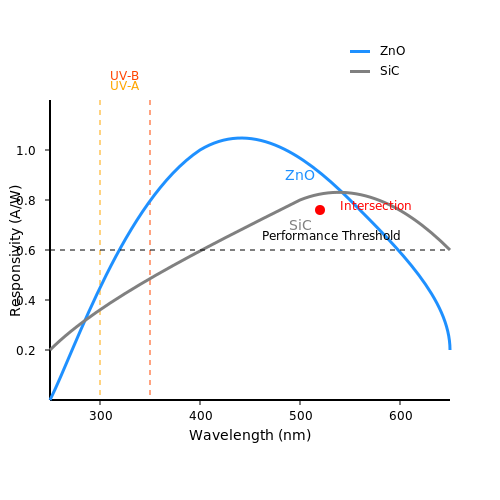
Zinc oxide (ZnO) exhibits a direct bandgap of ~3.37 eV, making it intrinsically sensitive to UV-A (320–400 nm) and UV-B (280–320 nm) radiation. Compared to silicon carbide (SiC, bandgap ~3.2 eV) and gallium nitride (GaN, ~3.4 eV), ZnO demonstrates superior exciton binding energy (60 meV vs. GaN's 25 meV), enabling higher quantum efficiency at room temperature. The responsivity (R) follows:
where η is quantum efficiency, q is electron charge, and λ is wavelength. ZnO typically achieves R > 0.2 A/W in the 300–370 nm range, outperforming SiC by 30–50% due to lower defect-mediated recombination.
Noise and Detectivity Comparison
The specific detectivity (D*) highlights ZnO's advantage in low-light applications:
where A is active area and In is noise current. ZnO photodetectors exhibit D* > 1012 Jones, surpassing commercial silicon-based UV-enhanced detectors (1010–1011 Jones) owing to ZnO's intrinsic dark current suppression. GaN devices, while comparable in detectivity, require complex epitaxial growth, increasing fabrication costs by 3–5×.
Response Speed and Spectral Selectivity
ZnO's electron mobility (~200 cm2/V·s) enables sub-nanosecond response times, critical for flame detection and optical communications. This outperforms organic photodetectors (e.g., P3HT:PCBM, τ > 10 ns) but lags behind GaN-based devices (τ ~ 100 ps) due to ZnO's higher trap density at grain boundaries. Spectral rejection ratios (UV/visible) exceed 104 for ZnO, compared to 102–103 for silicon carbide, attributed to ZnO's steeper absorption edge.
Environmental Stability and Cost
Unlike organic semiconductors (e.g., pentacene), ZnO demonstrates negligible photodegradation after 103 hours of UV exposure. Solution-processed ZnO films achieve 80% of single-crystal performance at <1% of the cost of molecular beam epitaxy-grown GaN, making them viable for large-area applications like UV index monitoring.
2. Thin-Film Deposition Methods
2.1 Thin-Film Deposition Methods
Sputtering
Radio-frequency (RF) and direct-current (DC) magnetron sputtering are widely used for depositing high-quality ZnO thin films. In RF sputtering, a high-frequency alternating field ionizes argon gas, creating a plasma that bombards the ZnO target, ejecting atoms that deposit onto the substrate. The process parameters—power, pressure, and substrate temperature—critically influence film stoichiometry and crystallinity. For instance, excessive oxygen partial pressure can lead to oxygen-rich films, degrading conductivity.
where P is power, MAr the argon mass, Ts substrate temperature, and d target-to-substrate distance.
Pulsed Laser Deposition (PLD)
PLD offers precise control over film composition by ablating a ZnO target with a high-energy laser pulse (typically KrF excimer, 248 nm). The ejected plasma plume condenses on the substrate, forming a crystalline film. The laser fluence (1–5 J/cm²) and repetition rate (1–10 Hz) determine the kinetic energy of ablated species, affecting grain size and defect density. PLD-grown ZnO films exhibit superior crystallinity, making them ideal for high-responsivity UV detectors.
Chemical Vapor Deposition (CVD)
Metal-organic CVD (MOCVD) uses precursors like diethylzinc (DEZn) and oxygen at elevated temperatures (300–600°C). The reaction:
enables large-area, uniform films with tunable dopant incorporation (e.g., Al, Ga) for conductivity modulation. Atmospheric-pressure CVD variants reduce equipment costs but require careful control of gas-phase reactions to prevent particle formation.
Atomic Layer Deposition (ALD)
ALD achieves atomic-scale thickness control through self-limiting surface reactions. Sequential exposure to zinc precursors (e.g., ZnCl2) and H2O at 100–200°C yields conformal films with minimal defects. The growth per cycle (GPC) is typically 0.1–0.2 nm/cycle, ideal for ultra-thin (<10 nm) active layers in heterojunction photodetectors. ALD’s low-temperature compatibility allows deposition on flexible substrates.
Spray Pyrolysis
A cost-effective solution-based method where a zinc salt precursor (e.g., zinc acetate) is atomized onto a heated substrate (350–450°C). Film properties depend on nozzle geometry, carrier gas flow, and precursor concentration. While less uniform than vacuum-based methods, spray pyrolysis is scalable for disposable UV sensors, achieving responsivities up to 10 A/W at 370 nm.
Comparative Analysis
- Sputtering/PLD: High crystallinity, but limited scalability.
- CVD/ALD: Excellent uniformity, higher equipment costs.
- Spray Pyrolysis: Low cost, trade-offs in defect density.
2.2 Nanostructured ZnO Fabrication
Nanostructured zinc oxide (ZnO) exhibits superior optoelectronic properties compared to bulk material due to quantum confinement effects and high surface-to-volume ratios. Several fabrication techniques enable precise control over morphology, crystallinity, and defect states, directly influencing UV photodetector performance.
Vapor-Phase Deposition Methods
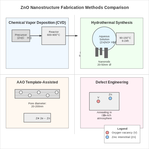
Chemical vapor deposition (CVD) enables high-purity ZnO nanostructure growth with tunable dimensions. The process involves zinc precursor vaporization (typically diethylzinc or zinc acetylacetonate) in an oxygen-rich environment at 400-800°C. The reaction proceeds via:
Varying the substrate temperature and carrier gas flow rate controls nanowire diameter (20-200 nm) and aspect ratio (10-100). Plasma-enhanced CVD further reduces growth temperatures below 300°C while maintaining crystalline quality.
Solution-Based Synthesis
Hydrothermal methods offer low-cost, scalable production of ZnO nanostructures. A typical process involves:
- Dissolving zinc nitrate hexahydrate (0.1M) and hexamethylenetetramine in deionized water
- Seeding substrates with ZnO nanoparticles via spin coating
- Reacting at 70-95°C for 2-12 hours
The pH-dependent growth kinetics follow:
where L is nanowire length, k0 is the pre-exponential factor, and Ea is activation energy (typically 35-50 kJ/mol).
Template-Assisted Fabrication
Anodic aluminum oxide (AAO) templates with 20-100 nm pore diameters enable ordered ZnO nanorod arrays. Electrodeposition parameters critically influence crystallinity:
| Parameter | Optimal Range | Effect |
|---|---|---|
| Potential | -0.8 to -1.2 V vs. Ag/AgCl | Controls nucleation density |
| Temperature | 60-80°C | Enhances carrier mobility |
| Zn2+ concentration | 0.01-0.1 M | Determines growth rate |
Defect Engineering
Controlled oxygen vacancies (VO) and zinc interstitials (Zni) modify carrier concentration. Post-growth annealing in forming gas (5% H2/95% N2) at 300-500°C introduces shallow donors, increasing conductivity while maintaining UV absorption:
where n is electron concentration and Nc is effective density of states in the conduction band.
2.3 Doping and Surface Modification Strategies
Doping Mechanisms in ZnO
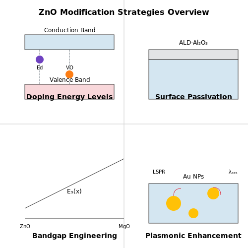
Doping ZnO with group-III (Al, Ga, In) or group-IV (Sn, Si) elements introduces shallow donor states near the conduction band, enhancing n-type conductivity. The ionization energy of these dopants can be approximated using effective mass theory:
where me* is the effective electron mass (0.28m0 for ZnO), and ϵr is the relative permittivity (8.5 for ZnO). For Al doping, this yields Ed ≈ 50 meV, ensuring near-complete ionization at room temperature.
Surface Passivation Techniques
Unpassivated ZnO surfaces exhibit oxygen vacancy (VO) defects acting as recombination centers. Atomic layer deposition (ALD) of Al2O3 reduces surface states by:
- Terminating dangling bonds with -OH groups
- Blocking atmospheric adsorbates
- Introducing negative fixed charges that repel minority carriers
The passivation quality is quantified by surface recombination velocity S:
where σ is capture cross-section, vth is thermal velocity, and Nt is trap density. ALD-Al2O3 reduces S from >105 cm/s to <103 cm/s.
Band Engineering via Alloying
MgxZn1-xO alloys (x ≤ 0.3) enable tunable bandgaps from 3.3 eV (pure ZnO) to 4.0 eV. The bowing parameter b modifies the bandgap prediction:
With b ≈ 1.8 eV, this allows precise cutoff wavelength control for solar-blind (λ < 280 nm) detection.
Plasmonic Enhancement
Embedding Au nanoparticles (5–20 nm diameter) creates localized surface plasmon resonances (LSPRs) that amplify UV absorption. The resonant wavelength λres follows:
where λp is the Au bulk plasmon wavelength (≈140 nm) and ϵm is the ZnO dielectric constant. Optimal nanoparticle spacing (30–50 nm) prevents coupling losses while maintaining field enhancement factors >10×.
3. Responsivity and Quantum Efficiency
3.1 Responsivity and Quantum Efficiency
The performance of a UV photodetector is primarily characterized by its responsivity (R) and quantum efficiency (η). These metrics determine how effectively the device converts incident photons into measurable electrical signals.
Responsivity
Responsivity (R) is defined as the photocurrent (Iph) generated per unit of incident optical power (Popt) at a given wavelength (λ):
For a photodetector operating in the UV range, R is typically expressed in units of A/W (amperes per watt). The responsivity depends on the material's absorption coefficient, carrier mobility, and device architecture. In zinc oxide (ZnO), the wide bandgap (~3.37 eV) ensures high UV selectivity, minimizing visible-light interference.
Quantum Efficiency
The external quantum efficiency (ηext) quantifies the fraction of incident photons that contribute to the photocurrent:
This can be expressed in terms of responsivity and photon energy (hν):
where h is Planck’s constant, ν is the photon frequency, and q is the electron charge. For ZnO UV photodetectors, ηext often exceeds 80% due to efficient electron-hole pair generation and low recombination losses.
Internal Quantum Efficiency
While ηext accounts for reflection and transmission losses, the internal quantum efficiency (ηint) describes charge carrier generation within the active layer:
Here, α is the absorption coefficient and d is the active layer thickness. Optimizing α and d is critical for maximizing ηint without introducing excessive dark current.
Practical Considerations
- Wavelength dependence: ZnO’s responsivity peaks near 370 nm, aligning with its bandgap.
- Bias voltage: Higher reverse bias increases carrier collection efficiency but may also elevate noise.
- Surface passivation: Reduces surface recombination, improving ηext.
Advanced device designs, such as nanostructured ZnO or hybrid heterojunctions, further enhance responsivity and quantum efficiency by leveraging light trapping and improved charge separation.
3.2 Response Time and Recovery Speed
The dynamic performance of a zinc oxide (ZnO) UV photodetector is primarily characterized by its response time and recovery speed, which determine how quickly the device reacts to changes in UV illumination and returns to its baseline state. These parameters are critical for applications requiring high-speed detection, such as optical communication, flame sensing, and military surveillance.
Response Time: Definition and Governing Factors
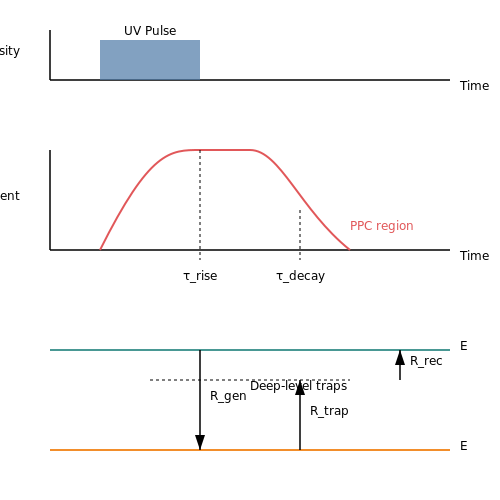
The response time (τrise) is defined as the time required for the photodetector's current to rise from 10% to 90% of its maximum value upon UV illumination. It is governed by:
where Rgen is the carrier generation rate and Rrec is the recombination rate. In ZnO photodetectors, the response time is influenced by:
- Carrier mobility: Higher electron mobility in ZnO (~200 cm²/V·s) reduces transit time.
- Defect density: Oxygen vacancies and zinc interstitials can trap carriers, slowing response.
- Device geometry: Smaller electrode gaps reduce drift time.
Recovery Speed: Trapping and Detrapping Dynamics
Recovery speed (τdecay) measures the time for the photocurrent to decay to 10% of its peak value after UV removal. It follows:
where Rtrap is the trapping rate. Persistent photoconductivity (PPC) in ZnO, caused by deep-level traps, often prolongs recovery. Strategies to mitigate this include:
- Surface passivation: Coating with Al2O3 reduces surface traps.
- Doping: Incorporating Mg or Ga suppresses oxygen vacancy formation.
- Bias voltage: Higher reverse bias accelerates carrier sweep-out.
Measurement Techniques
Response and recovery are typically measured using:
- Pulsed UV LEDs: Nanosecond pulses quantify ultrafast dynamics.
- Oscilloscope monitoring: Records real-time current transients.
- Chopper-wheel setups: Mechanically modulates UV for millisecond resolution.
Performance Benchmarks
State-of-the-art ZnO photodetectors achieve:
- τrise as low as 20 ns (for nanowire devices).
- τdecay under 100 µs (with optimized annealing).
For comparison, commercial Si-based UV detectors typically exhibit τrise > 1 µs due to indirect bandgap limitations.
3.3 Dark Current and Noise Performance
The dark current in a ZnO-based UV photodetector is the residual current that flows through the device in the absence of illumination. It arises primarily from thermal generation of charge carriers and defect-mediated conduction mechanisms. Minimizing dark current is critical for achieving high signal-to-noise ratio (SNR) and detectivity (D*), particularly in low-light applications.
Sources of Dark Current
Dark current in ZnO photodetectors originates from several mechanisms:
- Thermionic emission over the Schottky barrier (if metal-semiconductor contacts are used).
- Defect-assisted tunneling, where mid-gap states introduced by oxygen vacancies or zinc interstitials facilitate carrier transport.
- Surface leakage due to unpassivated dangling bonds or adsorbates.
- Bulk recombination-generation via Shockley-Read-Hall (SRH) centers.
The total dark current density (Jdark) can be modeled as a superposition of these contributions:
Noise Mechanisms
Noise in ZnO UV photodetectors limits the minimum detectable optical power and is governed by:
- Shot noise: Arises from the discrete nature of charge carriers and is proportional to the square root of the total current.
- Johnson-Nyquist (thermal) noise: Generated by thermal agitation of carriers in resistive components.
- 1/f (flicker) noise: Dominates at low frequencies due to defects and interface traps.
The total noise current spectral density (SI) is given by:
where q is the electron charge, kB is Boltzmann’s constant, T is temperature, R is the detector resistance, and Kf, α, β are empirical flicker noise parameters.
Impact on Detectivity
The specific detectivity (D*), a key figure of merit, is inversely proportional to the noise-equivalent power (NEP) and depends critically on dark current and noise performance:
where R is responsivity, A is the active area, and Δf is the bandwidth. Strategies to enhance D* include reducing defect density via improved ZnO growth techniques and optimizing device geometry to minimize leakage paths.
Practical Mitigation Techniques
Several approaches are employed to suppress dark current and noise in ZnO photodetectors:
- Surface passivation using Al2O3 or SiO2 to reduce surface recombination.
- Doping and annealing to minimize bulk defects.
- Heterostructure design (e.g., ZnO/MgZnO quantum wells) to enhance carrier confinement.
4. Schottky Barrier Photodetectors
4.1 Schottky Barrier Photodetectors
Operating Principle
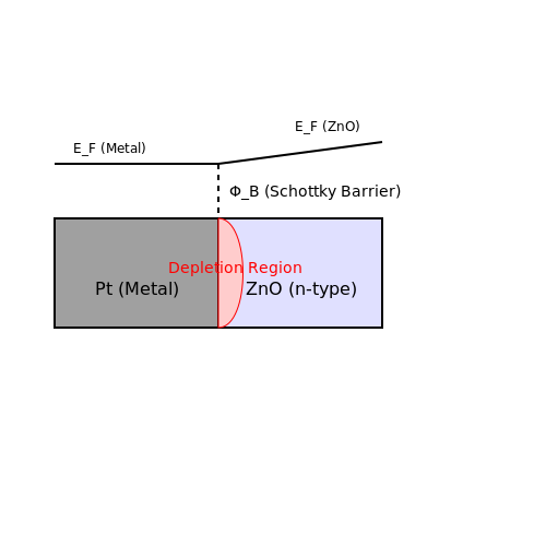
Schottky barrier photodetectors operate based on the rectifying properties of a metal-semiconductor junction. When a metal with a high work function (e.g., Au, Pt) contacts an n-type zinc oxide (ZnO) semiconductor, a Schottky barrier forms due to the difference in Fermi levels. Under UV illumination, electron-hole pairs are generated in the depletion region, and the built-in electric field separates them, producing a photocurrent.
where Jph is the photocurrent density, q is the electron charge, η is the quantum efficiency, Φ is the photon flux, R is the reflectivity, α is the absorption coefficient, and d is the depletion width.
Key Advantages
- Fast response time: Due to the majority carrier transport mechanism, Schottky detectors exhibit sub-nanosecond response times.
- Low dark current: The high barrier height minimizes thermionic emission, reducing noise.
- Simple fabrication: Requires only a metal-semiconductor junction, avoiding complex doping profiles.
Performance Metrics
The responsivity (R) and detectivity (D*) are critical figures of merit:
where Popt is the incident optical power, A is the detector area, Δf is the bandwidth, and In is the noise current.
Material Considerations
The choice of metal affects the barrier height (ΦB). For ZnO, common metals include:
- Platinum (Pt): High work function (~5.7 eV), yielding a large ΦB (~0.9 eV).
- Gold (Au): Moderate work function (~5.1 eV), with ΦB ~0.6 eV.
- Silver (Ag): Lower work function (~4.3 eV), resulting in a smaller barrier (~0.3 eV).
Challenges and Mitigations
Surface states at the metal-ZnO interface can pin the Fermi level, reducing the effective barrier height. Passivation techniques, such as atomic layer deposition (ALD) of Al2O3, can minimize this effect. Additionally, edge leakage can be suppressed by implementing guard rings or mesa isolation.
Applications
Schottky barrier ZnO photodetectors are used in:
- UV flame detection: Fast response is critical for industrial safety systems.
- Space-based sensors: Low dark current enables high sensitivity in low-light conditions.
- Optical communications: High-speed operation suits short-wavelength data transmission.
4.2 Metal-Semiconductor-Metal (MSM) Structures
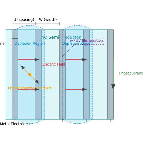
Metal-Semiconductor-Metal (MSM) photodetectors are widely employed in UV sensing due to their simple fabrication process, high responsivity, and compatibility with high-speed applications. The structure consists of interdigitated metal electrodes deposited on a semiconductor substrate, forming back-to-back Schottky contacts. When biased, photogenerated carriers are swept by the electric field, producing a measurable photocurrent.
Working Principle
The operation of an MSM photodetector relies on the formation of Schottky barriers at the metal-semiconductor interface. Under illumination, incident UV photons with energy exceeding the bandgap of zinc oxide (ZnO) generate electron-hole pairs. The applied bias creates a depletion region, separating the carriers and inducing a photocurrent. The responsivity R is given by:
where Iph is the photocurrent, Popt is the incident optical power, η is the quantum efficiency, q is the electron charge, λ is the wavelength, h is Planck’s constant, and c is the speed of light.
Key Parameters and Optimization
The performance of MSM photodetectors is influenced by several factors:
- Schottky Barrier Height: Determines the dark current and spectral response. For ZnO, metals like Au, Pt, and Ni provide suitable barrier heights.
- Electrode Geometry: Finger width and spacing affect the electric field distribution and carrier collection efficiency.
- Bias Voltage: Higher voltages improve carrier drift velocity but may increase dark current.
Transient Response and Bandwidth
The speed of an MSM photodetector is governed by the carrier transit time ttr and the RC time constant. The transit time is approximated by:
where d is the inter-electrode spacing, μ is the carrier mobility, and E is the electric field. The bandwidth BW is inversely proportional to the total response time:
Challenges and Mitigation Strategies
Despite their advantages, MSM photodetectors face challenges such as:
- Surface Recombination: Can be minimized by surface passivation techniques like atomic layer deposition (ALD) of Al2O3.
- Low Gain: Unlike p-n or p-i-n photodiodes, MSM structures lack intrinsic gain mechanisms unless avalanche multiplication is employed.
- Fabrication Defects: Precise lithography is required to avoid short circuits between electrodes.
Applications in UV Sensing
MSM photodetectors are extensively used in:
- UV Flame Detection: Due to their fast response and solar-blind operation.
- Optical Communications: High-speed MSM detectors enable UV-based free-space communication.
- Biological Sensing: Their sensitivity to UV-C wavelengths makes them suitable for sterilization monitoring.
4.3 p-n and p-i-n Junction Photodetectors
Working Principle of p-n Junction Photodetectors
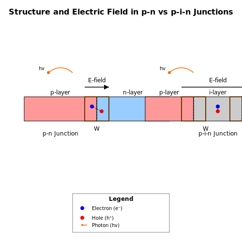
In a p-n junction photodetector, the built-in electric field at the junction separates photogenerated electron-hole pairs when illuminated with UV light. The depletion region width (W) is critical for efficient carrier collection and is given by:
where εs is the semiconductor permittivity, Vbi is the built-in potential, V is the applied bias, q is the electron charge, and NA, ND are the acceptor and donor concentrations, respectively.
p-i-n Junction Photodetectors
p-i-n photodetectors incorporate an intrinsic (i) region between the p- and n-layers, widening the depletion region and enhancing UV absorption. The responsivity (R) is derived from the quantum efficiency (η) and photon energy (hν):
where λ is the wavelength, h is Planck’s constant, and c is the speed of light. The intrinsic layer’s low doping reduces dark current, improving the detectivity (D*):
where A is the active area and Δf is the bandwidth.
Performance Comparison
Key differences between p-n and p-i-n structures include:
- Response Time: p-i-n junctions exhibit faster response due to reduced capacitance from the intrinsic layer.
- Dark Current: p-i-n detectors achieve lower dark currents (~nA) compared to p-n junctions (~µA).
- Spectral Selectivity: The intrinsic layer’s thickness can be tuned for optimal UV absorption.
Fabrication Techniques
ZnO-based p-n and p-i-n junctions are fabricated via:
- Molecular Beam Epitaxy (MBE): Ensures high crystallinity for low defect densities.
- Sputtering: Cost-effective for large-area deposition.
- Doping Strategies: Nitrogen or phosphorus for p-type ZnO; aluminum or gallium for n-type.
Applications
These photodetectors are used in:
- UV Imaging: High-speed imaging in astronomy and military surveillance.
- Flame Detection: Sensitive to UV emissions from combustion.
- Biological Sensing: DNA/RNA analysis due to ZnO’s biocompatibility.
Challenges
Despite advantages, challenges persist:
- p-type Doping Stability: ZnO’s native n-type dominance complicates reliable p-type doping.
- Interface Defects: Trap states at junctions can degrade responsivity.
- Scalability: Uniform doping over large areas remains difficult.
5. Environmental and Industrial Monitoring
5.1 Environmental and Industrial Monitoring
Zinc oxide (ZnO) UV photodetectors have emerged as critical components in environmental and industrial monitoring due to their high sensitivity, fast response times, and stability under harsh conditions. Their wide bandgap (~3.37 eV) enables selective UV detection, making them ideal for applications where precise UV intensity measurement is required.
Mechanisms of UV Detection in ZnO
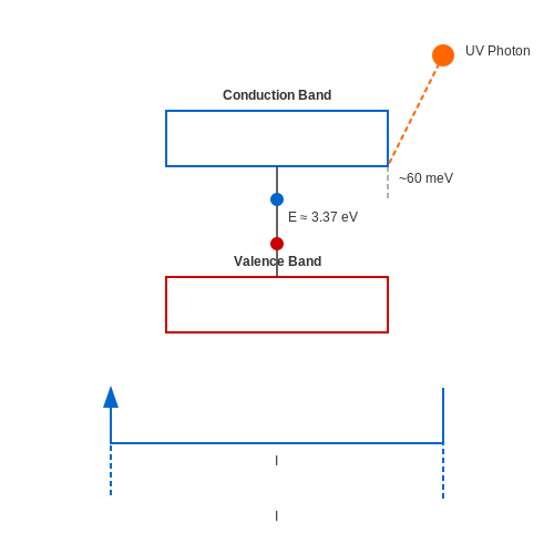
The photoconductive mechanism in ZnO relies on electron-hole pair generation under UV illumination. When photons with energy exceeding the bandgap are absorbed, electrons are excited from the valence band to the conduction band, increasing conductivity. The responsivity (R) of the detector is given by:
where Iphoto is the photocurrent, Idark is the dark current, and Popt is the incident optical power. The high exciton binding energy (~60 meV) of ZnO enhances UV absorption efficiency, leading to superior signal-to-noise ratios.
Environmental Monitoring Applications
ZnO UV photodetectors are extensively used in:
- Ozone Layer Monitoring: Detecting UV-B (280–315 nm) and UV-C (100–280 nm) radiation to assess ozone depletion.
- Pollution Sensing: Measuring UV absorption by airborne pollutants like NO2 and SO2.
- Solar UV Index Measurement: Providing real-time data for public health advisories.
Their robustness against temperature fluctuations and humidity makes them suitable for outdoor deployment in weather stations and satellite-based sensors.
Industrial Process Control
In industrial settings, ZnO UV detectors ensure:
- UV Curing Monitoring: Verifying proper exposure in adhesive and coating processes.
- Flame Detection: Identifying UV emissions from combustion in furnaces and engines.
- Water Sterilization: Validating UV lamp output in disinfection systems.
The fast response time (< 1 ms) of ZnO-based detectors allows real-time feedback in high-speed manufacturing lines.
Case Study: ZnO Nanowire Arrays for Enhanced Sensitivity
Recent advancements utilize vertically aligned ZnO nanowires to increase surface area and light trapping. The photocurrent gain (G) in such structures is modeled as:
where τn is the carrier lifetime and τt is the transit time. Nanowire configurations have demonstrated responsivities exceeding 105 A/W under 365 nm illumination, enabling detection of sub-nW/cm2 UV fluxes.
Integration with IoT Systems
Modern implementations combine ZnO photodetectors with wireless sensor networks for distributed monitoring. A typical node includes:
- A ZnO thin-film or nanowire detector.
- Transimpedance amplification circuitry.
- LoRa or NB-IoT transmitters for cloud-based analytics.
This enables large-scale deployment in smart cities for air quality mapping and industrial IoT for predictive maintenance of UV-dependent processes.
5.2 Biomedical UV Sensing Applications
Zinc oxide (ZnO) UV photodetectors have emerged as critical components in biomedical applications due to their high sensitivity, biocompatibility, and tunable spectral response in the ultraviolet range (200–400 nm). Their unique optoelectronic properties enable precise detection of UV radiation, which is essential in medical diagnostics, therapeutic monitoring, and sterilization processes.
UV-Induced Skin Cancer Detection
Excessive UV exposure is a leading cause of skin cancer, particularly melanoma. ZnO-based photodetectors integrated into wearable devices enable real-time monitoring of UV radiation dosage. The photodetector's responsivity (R) in the UVB range (280–315 nm) is given by:
where Iph is the photocurrent and Popt is the incident optical power. ZnO's wide bandgap (~3.37 eV) ensures minimal interference from visible light, enhancing signal-to-noise ratio in clinical settings.
Sterilization and Disinfection Monitoring
UV-C radiation (100–280 nm) is widely used for sterilizing medical equipment and air purification systems. ZnO photodetectors with high quantum efficiency in this range provide feedback on UV dosage, ensuring effective pathogen inactivation. The inactivation efficiency (η) follows a logarithmic dependence on UV fluence (F):
where k is the microorganism-specific inactivation constant. ZnO detectors calibrated to F thresholds ensure compliance with medical sterilization standards (e.g., ISO 15858).
Phototherapy Dosimetry
In UV phototherapy for conditions like psoriasis and vitiligo, precise dosage control is critical. ZnO photodetectors embedded in treatment arrays measure erythemal-weighted UV irradiance, minimizing overdose risks. The effective irradiance (Eeff) is calculated as:
where E(λ) is spectral irradiance and S(λ) is the erythemal action spectrum. ZnO's linear response curve ensures accurate dose accumulation over treatment sessions.
Case Study: Implantable UV Sensors
Recent advances in flexible ZnO nanostructures have enabled implantable UV sensors for post-surgical monitoring. These devices track UV exposure at wound sites to prevent photoaggravation of healing tissue. A 2023 study demonstrated a nanoporous ZnO sensor with:
- Response time < 50 ms
- Rejection ratio (UV/visible) > 104
- Biodegradation rate tunable from 7–90 days
The sensor's output correlates with localized UV index through a polynomial calibration curve derived from in-vivo trials.
Challenges in Biomedical Integration
While promising, ZnO UV detectors face hurdles in clinical adoption:
- Long-term stability: Protein fouling alters responsivity in biological fluids
- Dynamic range: Must simultaneously detect therapeutic (1–100 mW/cm²) and environmental (0.1–10 µW/cm²) UV levels
- Biocompatibility: Zn2+ ion leaching must remain below 50 µg/mL (per ISO 10993-5)
Ongoing research focuses on Al-doped ZnO and core-shell nanostructures to address these limitations while maintaining the material's inherent advantages for biomedical UV sensing.
5.3 Integration with Flexible Electronics
The integration of zinc oxide (ZnO) UV photodetectors with flexible electronics presents unique opportunities for wearable sensors, foldable displays, and conformal biomedical devices. ZnO’s inherent mechanical flexibility, combined with its wide bandgap (≈3.37 eV) and high exciton binding energy (60 meV), makes it an ideal candidate for stretchable optoelectronics. However, challenges such as strain-induced performance degradation and interfacial adhesion must be addressed.
Mechanical and Electrical Considerations
When ZnO thin films are deposited on flexible substrates like polyethylene terephthalate (PET) or polyimide (PI), mechanical strain alters their electronic properties. The piezotronic effect in ZnO—where strain modulates carrier transport—can be exploited for strain-gated photodetectors. The responsivity (R) under tensile strain (ε) follows:
where R0 is the unstrained responsivity and γ is the strain sensitivity coefficient (typically 10–100 for ZnO). Compressive strain, however, may induce cracking, necessitating optimized film thickness (<100 nm) or nanostructured morphologies (e.g., nanowires) for durability.
Substrate and Interface Engineering
Flexible substrates introduce thermal expansion mismatches with ZnO, leading to delamination. Solutions include:
- Buffer layers: Thin Al2O3 or SiO2 interlayers reduce stress and improve adhesion.
- Nanocomposites: Embedding ZnO nanoparticles in elastomers (e.g., PDMS) enhances stretchability while maintaining photoresponse.
- Neutral plane design: Positioning the active layer at the mechanical neutral axis minimizes strain during bending.
Fabrication Techniques
Low-temperature processes (<150°C) are critical for compatibility with plastic substrates:
- Sputtering: RF magnetron sputtering yields uniform ZnO films with controlled oxygen vacancies.
- Solution processing: ZnO sol-gel or nanoparticle inks enable roll-to-roll printing.
- Transfer printing: Pre-fabricated ZnO nanostructures can be transferred onto flexible substrates via sacrificial layers.
Performance Metrics Under Flexure
Key parameters degrade with bending radius (r). For a typical ZnO nanowire photodetector on PET:
where Iph0 is the initial photocurrent, t is substrate thickness, and k is a material constant (≈0.1 for ZnO/PET). Repeated bending cycles (>10,000 at r = 5 mm) show <10% responsivity loss in optimized designs.
Applications in Wearable Systems
ZnO UV photodetectors integrated into textiles monitor real-time UV exposure. A hybrid structure with graphene electrodes achieves a detectivity (D*) of 1012 Jones at 360 nm wavelength, even under 30% tensile strain. For biomedical patches, ZnO’s biocompatibility enables UV-sensitive wound healing monitors.
6. Key Research Papers and Reviews
6.1 Key Research Papers and Reviews
- Recent advancements in pure and doped zinc oxide nanostructures for UV ... — The electronic properties of zinc oxide can be improved by doping copper, and aluminum [57]. Cadmium (Cd) doped zinc oxide band gap energy is less (3.0eV) and magnesium (Mg) doped zinc oxide band gap energy is more (4.0eV) than pure zinc oxide [58]. Doping significantly influences the properties of ZnO-based UV photodetectors by modifying its ...
- Zinc oxide ultraviolet photodetectors: rapid progress from conventional ... — Zhang's group fabricated a p-NiO/n-ZnO NRs self-powered UV PD (Fig. 12d, device schematic). 191 A significant enhancement in the current was observed upon exposure to UV illumination (355 nm) at zero bias voltage (Fig. 12e, I-V characteristics in both the dark and UV states) and Fig. 12f shows its photoresponses at different UV illumination ...
- PDF High-performance Ultraviolet Photodetectors Based on ZnO Nanostructures — nanowires exhibit great promise for the highly efficient UV photodetectors. nanorods on ITO substrates by aqueous solution. The . Index Terms — zinc oxide, nanowires, UV-photodetector . I. INTRODUCTION ZnO is a semiconductor with wide direct band gap energy of 3.35 eV and a large exciton binding energy of 60 meV at room temperature [1]-[3].
- Research advances in ZnO nanomaterials-based UV photode ... - PubMed — Ultraviolet photodetectors (UV PDs) have always been the research focus of semiconductor optoelectronic devices due to their wide application fields and diverse compositions. As one of the best-known n-type metal oxides in third-generation semiconductor electronic devices, ZnO nanostructures and their assembly with other materials have received ...
- (PDF) Ultraviolet photodetection characteristics of Zinc oxide thin ... — Ultraviolet (UV) photoconductive sensors were fabricated using an aluminium (Al)-doped zinc-oxide (ZnO) nanorod array with a diameter between 40 and 150 nm and thickness of approximately 1.1 mum.
- Zinc oxide ultraviolet photodetectors: rapid progress from conventional ... — 1. Introduction In the past decade, the global consumption of energy and the population have increased significantly; this has prompted the development of energy-efficient, sustainable optical energy detection systems. 1-7 Among the energy detection systems, presently, ultraviolet (UV) photodetectors (PDs) have drawn potential applications in society, the scientific community and military ...
- (PDF) High-performance Ultraviolet Photodetectors Based on ZnO ... — PDF | On Jan 1, 2018, S. Noothongkaew and others published High-performance Ultraviolet Photodetectors Based on ZnO Nanostructures | Find, read and cite all the research you need on ResearchGate
- Recent Advances in Solution-Processed Zinc Oxide Thin Films for ... — As key components in high-speed optoelectronics, photodetectors with bandwidths greater than 100 GHz have been a topic of intense research for several decades. Solely InP-based detectors could ...
- Recent Advances in Solution-Processed Zinc Oxide Thin Films for ... — Zinc oxide (ZnO) is versatile among semiconducting metal oxides with properties such as high photosensitivity, highly tunable specific surface area, nontoxicity, piezoelectricity, almost 85% optical transparency in the visible region, large exciton binding energy, and good biocompatibility. ZnO also shows excellent chemical and thermal stability. This n-type semiconducting material finds ...
- Enhanced ultraviolet photodetection with Ag ... - ScienceDirect — Metal oxide semiconductors, particularly ZnO, have been extensively investigated for UV photodetectors due to their favorable physiochemical stability [2]. ZnO exhibits a large bandgap of 3.35 eV, significant exciton binding energy (60 meV), higher saturated carrier drift rate, enhanced radiation hardness, and optical properties similar to GaN ...
6.2 Textbooks on Semiconductor Photodetectors
- Zinc oxide ultraviolet photodetectors: rapid progress from conventional ... — Zinc oxide ultraviolet photodetectors: rapid progress from conventional to self-powered photodetectors ... 3.1.1 Conventional metal-semiconductor-metal-based UV photodetectors. In the past decade, pristine ZnO oxide nanomaterials in conventional metal-semiconductor-metal (MSM) PDs have been widely applied for the detection of UV light ...
- Zinc Oxide Materials for Electronic and Optoelectronic Device ... — 11.3 ZnO Film-Based UV Photodetectors 297. 11.3.1 Photoconductive UV Detector 297. 11.3.2 Schottky Barrier UV Photodetectors 301. 11.3.3 Integrated Surface Acoustic Wave and Photoconductive Wireless UV Detectors 305. 11.3.4 Photodetectors Using ZnO TFT 314. 11.3.5 MgxZn1_xO UV Photodetector 315. 11.4 ZnO NW UV Photodetectors 318
- Zinc oxide ultraviolet photodetectors: rapid progress from conventional ... — Journals & Books; Help. Search. My account. Sign in. Search ScienceDirect. Nanoscale Advances. Volume 1, Issue 6, 11 June 2019, Pages 2059-2085. Zinc oxide ultraviolet photodetectors: rapid progress from conventional to self-powered photodetectors. Author links ... where under UV illumination on a wide band gap semiconductor, the absorption of ...
- PDF Zinc oxide ultraviolet photodetectors: rapid progress from conventional ... — Zinc oxide ultraviolet photodetectors: rapid progress from conventional to self-powered photodetectors Buddha Deka Boruah * Currently, the development of ultraviolet (UV) photodetectors (PDs) has attracted the attention of the research community because of the vast range of applications of photodetectors in modern society. A
- Photodetectors: Devices, Circuits and Applications: Front Matter — 5.2.8.3 Resonant Cavity Enhanced Photodetectors 141 5.2.8.4 Quantum well Photodetectors 141 5.2.9 Photodiodes Packaging 142 5.2.10 Photodiode Specifications and Parameters 142 5.3 Photodiode Circuits 145 5.3.1 Circuits for Instrumentation Applications 146 5.3.1.1 Transimpedence Circuit 146
- A Comprehensive Review of Semiconductor Ultraviolet Photodetectors ... — Monoclinic gallium oxide (β-Ga 2 O 3) semiconductor, with the wide bandgap of ∼4.9 eV in the deep UV region, is one of the most promising candidates for high-performance UV photodetectors. Individual β -Ga 2 O 3 nanostructures such as nanobelts and nanowires, have been demonstrated by several reports to be potential solar-blind UV ...
- Ultraviolet Photodetectors: From Photocathodes to Low-Dimensional ... — Developing diamond-based UV photodetectors enabled detection in the range between UV and visible, with a short cut-off wavelength of λ c = 225 nm and high contrast (6 orders of magnitude) . Diamond is characterized by numerous extraordinary properties among all semiconductors, such as the highest mechanical hardness.
- PDF Fundamentals of zinc oxide as a semiconductor - University of Chicago — Rep. Prog. Phys. 72 (2009) 126501 A Janotti andCGVandeWalle A L Γ A H Γ-8-6-4-2 0 2 4 6 8 10 Energy (eV) K Zn O a c [0001] (a) (b) M Figure 1. The wurtzite crystal structure of ZnO with the lattice parameters a and c indicated in (a), and the calculated band structure of ZnO using the HSE hybrid functional in (b).The energy of the valence-band maximum (VBM) was set to zero.
- Zinc oxide heterostructures: advances in devices from self-powered ... — Zinc oxide (ZnO) is an universally known semiconductor in the field of blue and ultraviolet (UV) optical devices due to its wide bandgap (E g) and large room temperature (RT) excitonic binding energy.1., 2., 3. The crystal structure of ZnO is categorized into zinc blende, wurtzite, and rocksalt, where under ambient conditions, the thermodynamically stable phase is the wurtzite one (ZnO ...
- Recent advances in ultraviolet photodetectors — In recent years, ultraviolet (UV) photodetectors (PDs) have received much attention in the various field of research due to wide range of industrial, …
6.3 Open Access Resources and Datasets
- Recent advancements in pure and doped zinc oxide nanostructures for UV ... — The electronic properties of zinc oxide can be improved by doping copper, and aluminum [57]. Cadmium (Cd) doped zinc oxide band gap energy is less (3.0eV) and magnesium (Mg) doped zinc oxide band gap energy is more (4.0eV) than pure zinc oxide [58]. Doping significantly influences the properties of ZnO-based UV photodetectors by modifying its ...
- Development of Tetrapod Zinc Oxide-Based UV Sensor for Precision ... — There has been significant progress in design and development of UV sensors based upon metal oxides and semiconducting metal oxides [11,12] that have shown promise for UV sensing platforms. Zinc oxide (ZnO) is a promising candidate for sensing UV light because it possesses a wide direct bandgap of 3.37 eV at room temperature, a large exciton ...
- Zinc oxide ultraviolet photodetectors: rapid progress from conventional ... — Currently, the development of ultraviolet (UV) photodetectors (PDs) has attracted the attention of the research community because of the vast range of applications of photodetectors in modern society. ... Zinc oxide ultraviolet photodetectors: rapid progress from conventional to self-powered photodetectors ... This article is Open Access ...
- Zinc oxide ultraviolet photodetectors: rapid progress from conventional ... — Open access. ABSTRACT. Currently, the development of ultraviolet (UV) photodetectors (PDs) has attracted the attention of the research community because of the vast range of applications of photodetectors in modern society. ... Wurtzite ZnO has a hexagonal structure belonging to the P6 3 mc space group with the lattice parameters of a = 0.3296 ...
- Visible-blind UV photodetectors using a polymer/ZnO ... - ScienceDirect — Polymer/ZnO nanocomposite is a good choice for fabricating flexible UV photodetectors. Park et al. fabricated UV photodetectors based on PVK/ZnO quantum dots modified by graphene layer, which exhibited good performance with an on/off ratio of 10 8 at 0.4 V under 365 nm light illumination [18].In 2016, Kang et al. fabricated a solution-processable UV photodetector based on ZnO/PVK nanocomposite.
- Enhanced UV Photodetector Efficiency with a ZnO/Ga2O3 Heterojunction — It is evident from observation that responsivity of a device shows a maximum value in the UV region, while it is reduced in the visible region for HTs. In the case of detectivity, the maximum value reached was 145 × 10 14 Hz 1/2 /W (at ∼200 nm) and 38 × 10 14 Hz 1/2 /W (at 300 nm) for Ga 2 O 3 -coated ZnO and bare ZnO HTs, respectively.
- An all-sputtered photovoltaic ultraviolet photodetector based on co ... — Zinc oxide (ZnO) with a wide bandgap of > 3.1 eV, a high electron mobility of ~ 200 cm 2 V −1 s −1, and an exciton binding energy of ~ 60 meV has proven to be an outstanding material for UV ...
- High-performance transparent AZO UV photodetectors — In this work, the fabrication of undoped ZnO (ZO) and 3 at.% aluminum (Al) doped ZnO (AZO) thin films (TFs) based transparent photodetectors (PDs) was reported. Both films were spin-coated on fluorine-doped tin oxide (FTO) substrates to investigate the influence of Al doping on the ultraviolet (UV) detection performance of the devices. The systematic characterizations reveal that Al doping ...
- Synthesis and characterization of Cu doped ZnO nanoparticles for stable ... — The rising demand for optoelectronic devices to be operable in adverse environments necessitates the sensing of ultraviolet (UV) radiation. Here, a highly sensitive, fast responding Cu doped zinc oxide nanoparticles (Nps) based UV photodetector (PD) is reported. For the first time, Cu doped ZnO Nps are grown via forced hydrolysis of acetate salt of metals in a polyol medium. Various ...
- Self-connected CuO-ZnO radial core-shell heterojunction nanowire arrays ... — The bandgap of such metal oxides can be tuned during their synthesis allowing tailored light absorption from the UV up to ... (99.995% purity), platinum (99.99% purity) and zinc oxide (99.999% purity) sputtering targets having a diameter of 2 inch were purchased from Kurt J. Lesker Company Ltd. (UK). ... supported from the Romanian Ministry of ...