Zinc Oxide Transparent Conductors
1. Basic Properties of Zinc Oxide
Basic Properties of Zinc Oxide
Zinc oxide (ZnO) is a wide-bandgap semiconductor with a direct bandgap of approximately 3.37 eV at room temperature, making it highly transparent in the visible spectrum. Its large exciton binding energy (~60 meV) enables efficient excitonic emission even at elevated temperatures, a property leveraged in optoelectronic applications such as UV light-emitting diodes (LEDs) and laser diodes.
Crystal Structure and Defect Chemistry
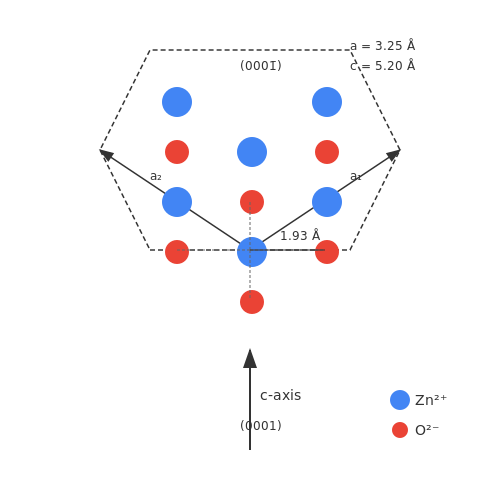
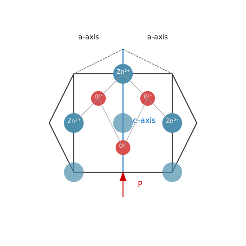
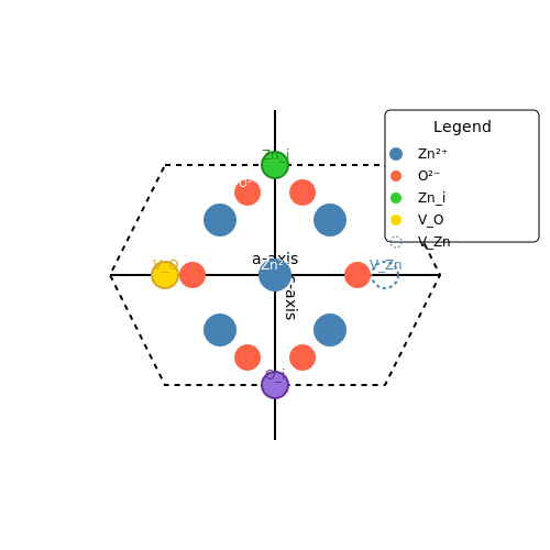
ZnO crystallizes primarily in the wurtzite structure (hexagonal, space group P63mc), though zincblende and rocksalt phases can be stabilized under specific conditions. The wurtzite form consists of alternating Zn2+ and O2- layers stacked along the c-axis, creating polar surfaces that influence growth morphology and defect formation.
Native defects dominate ZnO's electronic properties:
- Zinc interstitials (Zni) and oxygen vacancies (VO) act as shallow donors, enabling n-type conductivity even in undoped material
- Zinc vacancies (VZn) and oxygen interstitials (Oi) create deep acceptors, complicating p-type doping
Electronic and Optical Properties
The conduction band minimum at the Γ-point derives primarily from Zn 4s orbitals, while the valence band maximum consists of O 2p orbitals with some Zn 3d hybridization. This results in:
Key optical characteristics include:
- High refractive index (~2.0 at 600 nm)
- Strong excitonic absorption near the band edge (α > 105 cm-1)
- Phonon modes at 437 cm-1 (E2high) and 583 cm-1 (A1 LO)
Electrical Transport
Undoped ZnO typically exhibits n-type conductivity with electron mobilities reaching 200 cm2/V·s in single crystals. The temperature-dependent conductivity follows:
where the activation energy Ea ranges from 30-150 meV depending on defect concentration. Aluminum and gallium doping can increase carrier concentrations beyond 1020 cm-3 while maintaining transparency.
Thermal and Mechanical Properties
With a Debye temperature of 440 K and thermal conductivity of 50 W/m·K (300 K), ZnO outperforms many transparent conductive oxides in heat dissipation. Its mechanical robustness (Young's modulus ~140 GPa) enables integration with flexible substrates when grown as thin films.
1.2 Transparency and Conductivity Mechanisms
Optical Transparency in Wide Bandgap Semiconductors
The transparency of zinc oxide (ZnO) in the visible spectrum arises from its wide direct bandgap of approximately 3.3 eV at room temperature. The optical absorption coefficient α follows the Tauc relation for direct bandgap materials:
where A is a constant, hν is photon energy, and Eg is the bandgap energy. For photon energies below 3.3 eV (wavelengths > 375 nm), ZnO exhibits minimal absorption, resulting in >80% transparency in thin films (100-200 nm thickness).
Electrical Conduction Mechanisms
Undoped ZnO is naturally n-type due to intrinsic defects, primarily oxygen vacancies (VO) and zinc interstitials (Zni). The conductivity can be enhanced through aliovalent doping with group III elements (Al, Ga, In) via the reaction:
where AlZn• represents an aluminum ion substituting a zinc site, donating one free electron. The carrier concentration n follows:
with Nd as donor density and Ed as donor ionization energy (~50 meV for Al-doped ZnO).
Mobility Limitations
Electron mobility in ZnO is primarily limited by:
- Ionized impurity scattering: Dominant at high doping concentrations (>1 at.%)
- Grain boundary scattering: Significant in polycrystalline films
- Polar optical phonon scattering: The primary intrinsic limitation at room temperature
The Matthiessen's rule gives the total mobility μ:
State-of-the-art ZnO:Al films achieve mobilities of 40-60 cm2/V·s at carrier concentrations of 5-10 × 1020 cm-3.
Burstein-Moss Effect
At high doping levels (>3 × 1020 cm-3), the Fermi level enters the conduction band, causing a blue shift in the optical absorption edge described by:
where m* is the effective mass (≈0.28me for ZnO). This effect can increase the apparent bandgap by 0.1-0.3 eV in heavily doped films.
Practical Optimization
The figure of merit for transparent conductors combines conductivity and transparency:
where T is transmittance at 550 nm and Rsh is sheet resistance. Optimal ZnO:Al films achieve ΦTC > 10-3 Ω-1, with 85% visible transmittance and Rsh < 10 Ω/sq.
1.3 Comparison with Other Transparent Conductors
Electrical and Optical Performance
Zinc oxide (ZnO)-based transparent conductors exhibit a unique balance between electrical conductivity and optical transparency, competing with industry standards such as indium tin oxide (ITO) and fluorine-doped tin oxide (FTO). The figure of merit for transparent conductors, ΦTC, combines sheet resistance (Rs) and optical transmittance (T):
For undoped ZnO, Rs typically ranges from 10−3 to 10−4 Ω·cm, while achieving >85% transmittance in the visible spectrum (400–700 nm). In contrast, ITO achieves lower sheet resistance (10−4–10−5 Ω·cm) but suffers from indium scarcity and mechanical brittleness. Aluminum-doped ZnO (AZO) offers comparable conductivity to ITO while maintaining superior flexibility and cost efficiency.
Material Stability and Environmental Impact
ZnO-based conductors demonstrate superior environmental stability compared to organic alternatives like PEDOT:PSS, which degrade under prolonged UV exposure. The wide bandgap (~3.3 eV) of ZnO minimizes absorption losses in the visible spectrum, unlike narrower-bandgap materials such as graphene oxide. However, ZnO is susceptible to hydrogen diffusion at elevated temperatures (>300°C), which can increase resistivity—a limitation not observed in FTO.
Deposition Techniques and Scalability
Magnetron sputtering of ZnO allows room-temperature deposition on flexible substrates, unlike ITO which often requires high-temperature annealing. Solution-processed ZnO nanoparticles enable roll-to-roll manufacturing at significantly lower cost than vacuum-deposited ITO. The table below compares key parameters:
| Material | Sheet Resistance (Ω/sq) | Avg. Transmittance (%) | Flexibility |
|---|---|---|---|
| ITO | 10–100 | 85–90 | Poor |
| AZO | 50–200 | 80–88 | Good |
| Graphene | 200–1000 | 90–97 | Excellent |
Emerging Alternatives and Hybrid Systems
Recent advances in silver nanowire networks achieve Rs < 10 Ω/sq with >95% transmittance, but suffer from oxidation and high cost. Hybrid ZnO/silver nanowire systems leverage the high conductivity of silver while using ZnO as a protective coating. Carbon nanotube-based conductors show promise for infrared transparency, where ZnO and ITO exhibit significant absorption.
Case Study: Solar Cell Applications
In thin-film photovoltaics, AZO outperforms ITO in damp heat tests (85°C/85% RH), showing <5% increase in Rs after 1000 hours, versus >30% for ITO. The lower refractive index of ZnO (1.9 vs. ITO's 2.0) also reduces Fresnel reflection losses at the TCO/active layer interface.
2. Chemical Vapor Deposition (CVD)
2.1 Chemical Vapor Deposition (CVD)
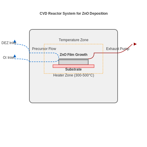
Chemical Vapor Deposition (CVD) is a high-precision thin-film deposition technique widely employed for synthesizing zinc oxide (ZnO) transparent conductive oxides (TCOs). The process involves the thermal decomposition or chemical reaction of volatile precursors in a gas-phase reaction, resulting in the deposition of a solid film on a heated substrate.
Process Mechanism
The CVD reaction for ZnO typically employs zinc-containing precursors such as diethylzinc (DEZ, Zn(C2H5)2) or dimethylzinc (DMZ, Zn(CH3)2), combined with an oxygen source (O2, H2O, or N2O). The overall reaction can be represented as:
The process occurs in several stages:
- Precursor vaporization: The liquid or solid precursor is vaporized and transported into the reaction chamber via a carrier gas (e.g., argon or nitrogen).
- Gas-phase reactions: The precursor molecules undergo pyrolysis or oxidation in the gas phase near the heated substrate.
- Surface adsorption and nucleation: Reactive species adsorb onto the substrate surface, forming nucleation sites for film growth.
- Film growth: Continued deposition leads to layer-by-layer growth, with the film morphology controlled by temperature, pressure, and precursor flow rates.
Key Process Parameters
The quality of ZnO films produced by CVD depends critically on several parameters:
- Substrate temperature: Typically ranges from 300°C to 600°C. Higher temperatures improve crystallinity but may increase defect concentrations.
- Chamber pressure: Low-pressure CVD (LPCVD) operates at 0.1-10 Torr, while atmospheric-pressure CVD (APCVD) runs at 760 Torr.
- Precursor ratio: The Zn:O precursor ratio affects stoichiometry, with oxygen-rich conditions reducing oxygen vacancies.
- Carrier gas flow rate: Controls the residence time of reactants and influences film uniformity.
Doping Strategies
To enhance conductivity, ZnO is commonly doped with group-III elements (Al, Ga, In) during CVD. The doping process can be described by:
Aluminum doping introduces additional charge carriers through the substitution of Zn2+ with Al3+, increasing the film's conductivity while maintaining transparency in the visible spectrum.
Advantages and Limitations
Advantages:
- High deposition rates (up to 100 nm/min)
- Excellent conformal coverage on complex geometries
- Precise control over stoichiometry and doping
- Scalable for industrial production
Limitations:
- High process temperatures may limit substrate choices
- Precursor toxicity and handling requirements
- Potential for gas-phase particle formation
Recent Developments
Plasma-enhanced CVD (PECVD) and atomic layer deposition (ALD) have emerged as variants offering lower-temperature processing and improved thickness control. PECVD, in particular, enables deposition at temperatures below 200°C by using plasma to activate precursor molecules.
2.2 Sputtering Techniques
Fundamentals of Sputtering Deposition
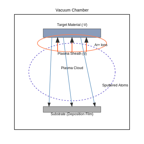
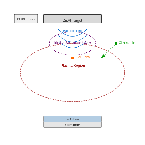
Sputtering is a physical vapor deposition (PVD) technique where atoms are ejected from a solid target material due to bombardment by high-energy ions, typically argon (Ar+). The ejected atoms then condense on a substrate to form a thin film. For zinc oxide (ZnO) transparent conductors, sputtering offers precise control over stoichiometry, crystallinity, and doping concentration, making it a preferred method for industrial applications.
The sputtering yield Y, defined as the number of target atoms ejected per incident ion, is given by:
where α is a dimensionless factor (~0.2 for typical materials), M1 and M2 are the masses of the incident ion and target atom respectively, Ei is the ion energy, and U0 is the surface binding energy of the target material.
Magnetron Sputtering Configurations
For ZnO deposition, magnetron sputtering is most commonly employed due to its high deposition rates and low substrate heating. The magnetic field confines electrons near the target surface, increasing ionization efficiency. Two primary configurations are used:
- DC Magnetron Sputtering: Suitable for conducting ZnO targets. Applied voltages typically range from 300–600 V with current densities of 5–20 mA/cm2.
- RF Magnetron Sputtering: Required for insulating targets (e.g., undoped ZnO). Operates at 13.56 MHz with power densities of 1–10 W/cm2.
Reactive Sputtering for Doped ZnO
Aluminum-doped zinc oxide (AZO) films are commonly deposited via reactive sputtering using a metallic Zn:Al target in an oxygen/argon atmosphere. The oxygen partial pressure pO2 critically affects film properties:
where ρ is resistivity, Ea is activation energy for dopant incorporation, and n is carrier concentration. Optimal pO2 ranges from 0.1–1.0 mTorr to balance oxygen vacancies (donors) and interstitial defects (scattering centers).
Process Optimization Parameters
Key sputtering parameters for high-quality ZnO films include:
| Parameter | Typical Range | Effect on Film Properties |
|---|---|---|
| Substrate Temperature | 25–300°C | Higher T improves crystallinity but may increase roughness |
| Sputtering Power | 50–300 W | Affects deposition rate and stoichiometry |
| Working Pressure | 1–10 mTorr | Lower pressure yields denser films |
| Target-to-Substrate Distance | 5–15 cm | Influences uniformity and residual stress |
Industrial Scaling Considerations
For large-area deposition (e.g., photovoltaic applications), rotating cylindrical targets and linear magnetron designs are employed. The deposition uniformity Δ across a substrate of width W follows:
where d(x) is local thickness and d̄ is average thickness. Modern systems achieve Δ > 95% for 2 m wide substrates using computer-controlled gas injection and multi-zone heating.
2.3 Sol-Gel Methods
The sol-gel process is a versatile wet-chemical technique for synthesizing zinc oxide (ZnO) thin films with controlled morphology, stoichiometry, and doping profiles. This method offers precise compositional tuning, low-temperature processing, and scalability for large-area transparent conductor applications.
Chemical Precursors and Reaction Mechanisms
The sol-gel synthesis of ZnO typically begins with zinc precursors such as zinc acetate dihydrate (Zn(CH3COO)2·2H2O) dissolved in alcoholic solvents. The hydrolysis and condensation reactions proceed as follows:
Dopants like aluminum (Al3+) or gallium (Ga3+) can be introduced during the sol formation stage by adding salts such as aluminum nitrate (Al(NO3)3) or gallium chloride (GaCl3). The substitutional doping mechanism follows:
Processing Parameters and Film Formation
Key variables influencing film properties include:
- Precursor concentration (0.1–0.5 M typical for ZnO)
- Solvent selection (methanol, ethanol, or 2-methoxyethanol)
- Stabilizers (monoethanolamine common for pH control)
- Aging time (12–72 hours for optimal viscosity)
Deposition occurs via spin-coating or dip-coating, with each layer typically 50–100 nm thick after thermal treatment. Multi-layer deposition builds the desired film thickness while maintaining optical clarity.
Thermal Treatment and Crystallization
Post-deposition annealing (300–600°C) drives solvent evaporation, organic removal, and crystallization into the hexagonal wurtzite structure. The crystallite size (D) follows the Scherrer equation:
where K is the shape factor (0.9), λ is the X-ray wavelength, β is the line broadening at FWHM, and θ is the Bragg angle.
Performance Optimization
Record conductivities (>1000 S/cm) are achieved through:
- Optimized doping concentrations (2–5 at.% Al)
- Controlled oxygen partial pressure during annealing
- Post-hydrogen treatment to passivate oxygen vacancies
Optical transparency >85% in the visible spectrum is maintained when carrier concentrations are kept below 5×1020 cm-3 to minimize free carrier absorption.
Advantages Over Sputtering and CVD
Compared to vacuum-based methods, sol-gel offers:
- Lower capital equipment costs
- Better compositional homogeneity for doped films
- Conformal coating on non-planar substrates
- Easier integration with roll-to-roll processing
Recent advances include inkjet-printed sol-gel ZnO for patterned transparent electrodes, achieving <5 Ω/sq sheet resistance with 92% transmittance at 550 nm.
2.4 Pulsed Laser Deposition (PLD)
Fundamentals of PLD
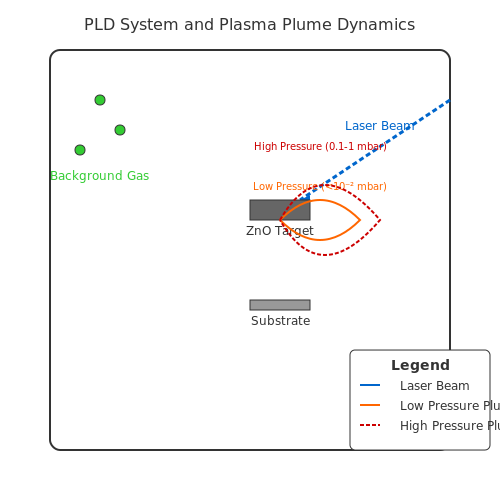
Pulsed Laser Deposition (PLD) is a thin-film growth technique where a high-power pulsed laser beam ablates a target material, creating a plasma plume that deposits onto a substrate. The process occurs in a vacuum or controlled gas environment, allowing precise stoichiometric transfer of complex materials like zinc oxide (ZnO). The key advantage of PLD is its ability to maintain the target's composition in the deposited film, critical for achieving high-quality ZnO transparent conductors with minimal defects.
Laser-Target Interaction and Plasma Formation
When an intense laser pulse (typically excimer lasers, e.g., KrF at 248 nm or ArF at 193 nm) strikes the ZnO target, energy absorption leads to rapid heating, vaporization, and ionization of the surface. The resulting plasma plume consists of ions, electrons, and neutral species with kinetic energies ranging from 1–100 eV. The ablation process can be modeled using the following thermal and non-thermal mechanisms:
where T is temperature, α is thermal diffusivity, I(t) is laser intensity, R is reflectivity, ρ is density, and Cp is heat capacity. For ZnO, the bandgap (3.37 eV) necessitates UV lasers for efficient absorption.
Plume Dynamics and Film Growth
The plasma plume expands adiabatically toward the substrate, with its angular distribution influenced by background gas pressure. At low pressures (< 10-2 mbar), the plume is forward-peaked, while higher pressures (0.1–1 mbar) induce scattering and thermalization. The deposition rate Rd depends on laser fluence F, repetition rate f, and target-substrate distance d:
where η is the ablation yield, mi is ion mass, and Tp is plume temperature. Optimal ZnO film conductivity is achieved at oxygen partial pressures of 10-3–10-2 mbar, balancing oxygen vacancies (donor defects) and lattice integrity.
Substrate Considerations and Crystallinity
ZnO films grown via PLD exhibit preferential c-axis orientation due to the lowest surface energy of (002) planes. Substrate choice (e.g., sapphire, glass, or silicon) and temperature (200–600°C) critically influence crystallinity. High-resolution XRD studies show that full-width-at-half-maximum (FWHM) of (002) peaks below 0.3° indicate excellent crystallinity, directly correlating with electron mobility > 50 cm2/V·s in doped ZnO.
Doping Strategies for Conductivity Enhancement
In-situ doping during PLD is achieved by using composite targets (e.g., ZnO:Al or ZnO:Ga) or dual-target ablation. For Al-doped ZnO (AZO), the solubility limit of ~2 at.% Al must be respected to avoid secondary phase formation. The carrier concentration n follows:
where ND and NA are donor and acceptor densities, ΔED is donor ionization energy (~30–60 meV for AlZn), and gA is degeneracy factor. Optimized PLD-grown AZO achieves resistivities below 5×10⁻⁴ Ω·cm with >80% visible transparency.
Challenges and Mitigation Strategies
Particulate formation during PLD remains a key challenge, addressed by off-axis deposition or velocity filters. Non-uniform plume distributions require substrate rotation for thickness homogeneity. Post-deposition annealing in forming gas (N2/H2) can further improve conductivity by passivating grain boundary traps while maintaining optical transparency.
3. Aluminum Doping (AZO)
3.1 Aluminum Doping (AZO)
Structural and Electronic Properties
Aluminum-doped zinc oxide (AZO) forms when Al3+ ions substitute Zn2+ sites in the wurtzite lattice. Each substitution introduces one additional electron into the conduction band due to the excess valence electron from aluminum. The carrier concentration n follows:
where [AlZn] is the aluminum concentration and f represents the fraction of compensating defects. The electron mobility μ in AZO is limited by ionized impurity scattering at high doping levels:
Optoelectronic Performance
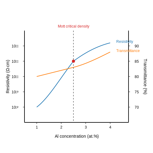
AZO achieves optimal transparency (>85% in visible spectrum) when carrier concentrations are maintained below the Mott critical density (~1020 cm-3). The plasma frequency ωp determines the onset of infrared reflectivity:
where m* is the effective mass (≈0.3me for ZnO). Practical AZO films demonstrate sheet resistances of 5-10 Ω/□ with >90% transparency when deposited by sputtering at 200-300°C.
Defect Chemistry
Aluminum incorporation is governed by the defect equilibrium:
Compensating oxygen interstitials (Oi′′) and zinc vacancies (VZn′′) become significant at doping levels >2 at.%, leading to mobility degradation. Secondary phase formation (ZnAl2O4) occurs beyond the solid solubility limit (~3 at.% Al).
Deposition Techniques
- Magnetron Sputtering: Reactive deposition from Zn:Al alloy targets in Ar/O2 atmospheres yields the highest mobilities (35-45 cm2/V·s)
- Pulsed Laser Deposition: Enables stoichiometric transfer at low temperatures (150-200°C) with minimal defect generation
- Atomic Layer Deposition: Provides conformal coatings with precise thickness control, though with higher resistivity
Stability Considerations
AZO films degrade under humid conditions due to hydrolysis reactions at grain boundaries. Passivation with thin SiO2 or Al2O3 overlayers (5-10 nm) improves environmental stability while maintaining sheet resistance within 10% of initial values after 1000 hours at 85°C/85% RH.
3.2 Gallium Doping (GZO)
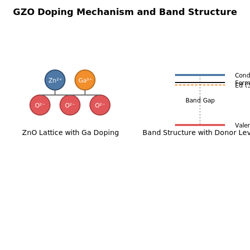
Gallium-doped zinc oxide (GZO) is a prominent alternative to indium-doped tin oxide (ITO) due to its comparable optoelectronic properties, lower cost, and reduced environmental impact. Gallium (Ga) serves as an effective n-type dopant in ZnO, introducing shallow donor states near the conduction band edge. The substitutional replacement of Zn2+ with Ga3+ donates a free electron, enhancing conductivity while maintaining high optical transparency in the visible spectrum.
Electronic Structure and Doping Mechanism
The doping efficiency of Ga in ZnO is governed by the defect chemistry and electronic band structure. Ga3+ (ionic radius ~0.62 Å) closely matches Zn2+ (~0.74 Å), minimizing lattice distortion. The donor ionization energy (Ed) is given by:
where e is the electron charge, ε0 is the vacuum permittivity, εr is the relative permittivity of ZnO (~8.5), and rd is the effective donor radius. For Ga in ZnO, Ed ≈ 30–60 meV, ensuring near-complete ionization at room temperature.
Optoelectronic Properties
GZO films achieve resistivities as low as 2×10⁻⁴ Ω·cm with carrier concentrations of ~1021 cm−3 and mobilities of 15–50 cm2/V·s. The optical transmittance exceeds 85% in the visible range (400–700 nm), with the plasma frequency (ωp) given by:
where n is the carrier density and m* is the effective mass (~0.28me for ZnO). The Burstein-Moss shift explains the widening of the optical bandgap (ΔEBM) due to Fermi-level lifting:
Deposition Techniques and Challenges
GZO is typically deposited via sputtering, pulsed laser deposition (PLD), or chemical vapor deposition (CVD). Sputtering with a ZnO:Ga2O3 target (1–5 wt% Ga) yields optimal homogeneity. Key challenges include:
- Oxygen vacancies (VO): Compensate donors, reducing mobility.
- Ga segregation: High doping (>4 at%) leads to Ga-rich grain boundaries.
- Hydrogen passivation: Ambient H2 can neutralize Ga donors.
Applications and Performance Metrics
GZO is used in:
- Thin-film solar cells (CIGS, perovskite) as front electrodes.
- Flexible displays due to ZnO's mechanical resilience.
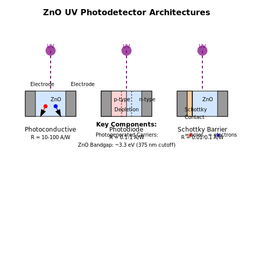
- UV photodetectors leveraging ZnO's wide bandgap.
Performance benchmarks for GZO vs. ITO:
| Property | GZO | ITO |
|---|---|---|
| Resistivity (Ω·cm) | 2×10⁻⁴ | 1×10⁻⁴ |
| Transmittance (550 nm) | 85–90% | 90–95% |
| Cost (per m2) | $$15–20 | $$50–70 |
3.3 Impact of Doping on Electrical and Optical Properties
The electrical and optical properties of zinc oxide (ZnO) transparent conductors are profoundly influenced by doping, which introduces extrinsic charge carriers and modifies the band structure. The most common dopants for n-type ZnO include group III elements (Al, Ga, In) and group IV elements (Sn, Si), while p-type doping remains challenging due to self-compensation effects.
Carrier Concentration and Mobility
Doping introduces additional charge carriers, increasing the conductivity (σ) according to:
where n is the carrier concentration, e is the electron charge, and μ is the mobility. For Al-doped ZnO (AZO), carrier concentrations can reach up to 1021 cm-3, with mobilities typically in the range of 20–50 cm2/V·s. The mobility is limited by ionized impurity scattering at high doping levels:
where T is temperature and NI is the ionized impurity concentration.
Optical Transparency and Band Gap Shifting
Heavily doped ZnO exhibits a blue shift in the optical band gap (Burstein-Moss effect) due to filling of conduction band states:
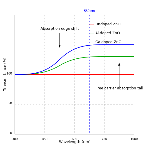
where m* is the effective mass. Simultaneously, doping-induced defects can create sub-bandgap absorption, particularly in the near-infrared region, due to free carrier absorption:
with p ≈ 2–3 for typical TCOs. Optimal doping balances these competing effects to maximize both conductivity and transparency.
Dopant Selection Criteria
The choice of dopant affects both electrical and optical performance:
- Aluminum (Al): Most common, but prone to oxidation and segregation at high concentrations.
- Gallium (Ga): Higher resistance to oxidation, with slightly lower mobility than Al-doped ZnO.
- Indium (In): Produces the highest mobilities but is costly and can form secondary phases.
The figure below compares the transmittance spectra of undoped and doped ZnO films, showing the characteristic absorption edge shift and free carrier absorption tail.
Non-Degenerate vs Degenerate Doping Regimes
At low doping levels (<1019 cm-3), ZnO behaves as a non-degenerate semiconductor with thermally activated conduction. Above the Mott critical density (~1019 cm-3), it transitions to degenerate behavior with metallic conduction, described by the Drude model:
where ωp is the plasma frequency and τ is the relaxation time. This transition significantly impacts both electrical and optical properties.
Stability and Environmental Effects
Doped ZnO films often exhibit property changes in humid environments due to chemisorption of water molecules at grain boundaries, which can passivate donor states. Accelerated aging tests show that Ga-doped ZnO generally demonstrates better environmental stability than Al-doped ZnO, making it preferable for outdoor applications.
4. Transparent Electrodes in Solar Cells
4.1 Transparent Electrodes in Solar Cells
Zinc oxide (ZnO) has emerged as a leading material for transparent conductive electrodes (TCEs) in solar cells due to its optimal balance of high optical transparency (>80% in the visible spectrum) and electrical conductivity (resistivity as low as 10−4 Ω·cm). Unlike indium tin oxide (ITO), ZnO offers cost-effectiveness, abundant raw materials, and tunable electronic properties via doping.
Optoelectronic Properties of ZnO
The performance of ZnO as a TCE is governed by its wide bandgap (~3.3 eV) and high carrier mobility. The optical transmittance T and sheet resistance Rs are derived from the Drude model for free-electron gases:
where Z0 is the impedance of free space (377 Ω), σop is the optical conductivity, and σdc is the DC conductivity. For optimal solar cell integration, a figure of merit (FOM) is used:
High-performance ZnO films achieve ΦTC > 10−3 Ω−1, rivaling ITO.
Doping Strategies for Enhanced Conductivity
Undoped ZnO exhibits n-type conductivity due to oxygen vacancies and zinc interstitials. Intentional doping further improves conductivity:
- Aluminum doping (AZO): Al3+ substitutes Zn2+, donating free electrons. Carrier concentrations reach ~1021 cm−3 with resistivity ~2×10⁻⁴ Ω·cm.
- Gallium doping (GZO): Ga3+ introduces fewer lattice distortions than Al, improving stability at high temperatures.
- Hydrogen plasma treatment: Passivates defects and increases carrier mobility up to 60 cm2/V·s.
Integration with Solar Cell Architectures
ZnO TCEs are compatible with multiple photovoltaic technologies:
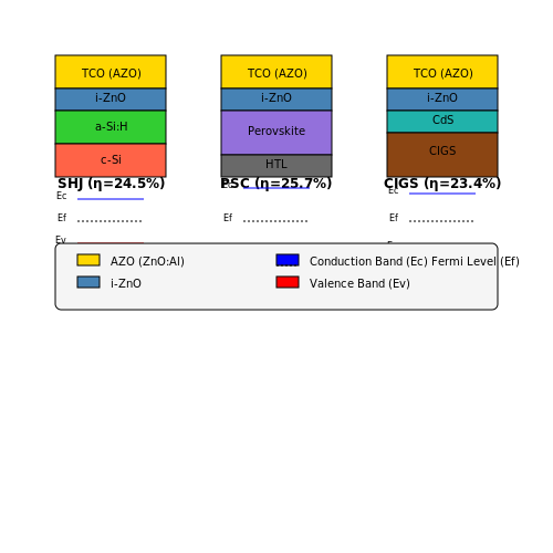
- Silicon heterojunction (SHJ) cells: AZO films serve as front electrodes, achieving >23% efficiency due to low parasitic absorption.
- Perovskite solar cells (PSCs): ZnO electron transport layers (ETLs) enable >25% efficiency by aligning energy levels (e.g., ZnO conduction band at −4.3 eV vs. vacuum).
- Organic photovoltaics (OPVs): Solution-processed ZnO nanoparticles reduce interface recombination losses.
Case Study: ZnO in CIGS Solar Cells
In Cu(In,Ga)Se2 (CIGS) cells, a bilayer of intrinsic ZnO (i-ZnO) and AZO minimizes recombination at the buffer/absorber interface. The i-ZnO (50–100 nm) acts as a high-resistivity buffer, while the AZO (500 nm) provides lateral conductivity. This configuration yields modules with >15% efficiency and <3% performance degradation over 1,000 hours under 85°C/85% RH damp heat testing.
Deposition Techniques
Film quality depends critically on the deposition method:
| Method | Advantages | Limitations |
|---|---|---|
| Magnetron sputtering | High density, industrial scalability | Requires post-annealing for optimal conductivity |
| Atomic layer deposition (ALD) | Atomic-level thickness control, conformal coatings | Low growth rate (~0.1 nm/s) |
| Spray pyrolysis | Low-cost, non-vacuum process | Higher defect density |
Recent advances include pulsed laser deposition (PLD) of AZO at room temperature, achieving resistivity of 4×10⁻⁴ Ω·cm without post-treatment.
Stability Challenges and Solutions
ZnO suffers from environmental degradation mechanisms:
- Hydrolysis: Surface reactions with H2O form Zn(OH)2, increasing resistivity. Al2O3 encapsulation layers (10 nm) reduce moisture ingress by 103×.
- Photocorrosion: UV exposure generates electron-hole pairs that oxidize ZnO. Nd doping increases corrosion resistance by shifting the Fermi level.
4.2 Flexible and Wearable Electronics
Mechanical Flexibility and Strain Tolerance
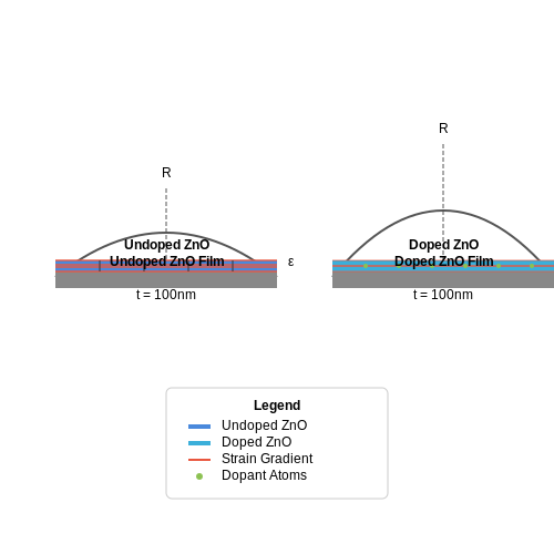
Zinc oxide (ZnO) thin films exhibit exceptional mechanical flexibility due to their polycrystalline or amorphous microstructure, making them ideal for flexible substrates. The critical bending radius Rc for ZnO films can be derived from the fracture strain limit εf and film thickness t:
For a typical ZnO film (t = 100 nm, εf ≈ 1%), Rc ≈ 5 mm, enabling conformal integration with curvilinear surfaces. Doping with aluminum (AZO) or gallium (GZO) further enhances strain tolerance by reducing grain boundary defects.
Optoelectronic Performance Under Deformation
The sheet resistance Rs of ZnO films under tensile strain ε follows a power-law dependence:
where α (≈ 5–10) and β (≈ 1.2–1.5) are empirically determined coefficients. Optical transparency (>80% at 550 nm) remains stable up to ε ≈ 2% due to the wide bandgap (3.37 eV) and minimal free-carrier absorption.
Integration Strategies for Wearable Systems
Key approaches for wearable integration include:
- Hybrid architectures: ZnO-polymer composites (e.g., ZnO-PEDOT:PSS) for enhanced flexibility.
- Island-bridge designs: Rigid ZnO islands interconnected by serpentine metal traces to localize strain.
- Neutral-plane engineering: Encapsulating ZnO layers near the mechanical neutral axis to minimize bending stress.
Case Study: Epidermal Electronics
ZnO-based transparent electrodes have been successfully integrated into skin-mounted sensors for continuous health monitoring. A 2023 study demonstrated a ZnO-Ag nanowire hybrid electrode with:
- Sheet resistance Rs < 20 Ω/sq after 10,000 bending cycles at R = 3 mm.
- Stable ECG signal acquisition under 15% skin deformation.
Challenges and Mitigation Strategies
Primary limitations:
- Environmental degradation: Hydrolysis at high humidity can be mitigated by atomic layer deposition (ALD) of Al2O3 barriers.
- Adhesion failure: Oxygen plasma treatment improves ZnO-polymer interfacial strength by 40%.
Recent advances in room-temperature sputtering and inkjet printing have enabled direct ZnO patterning on temperature-sensitive substrates like polyethylene terephthalate (PET) and polyimide (PI).
4.3 Display Technologies
Zinc oxide (ZnO)-based transparent conductive oxides (TCOs) are increasingly employed in display technologies due to their high optical transparency (>80% in the visible spectrum) and low electrical resistivity (10−4–10−3 Ω·cm). Unlike indium tin oxide (ITO), ZnO offers superior mechanical flexibility, making it suitable for next-generation flexible displays.
Electro-Optical Performance in Displays
The figure of merit (FOM) for transparent conductors in displays is given by the Haacke equation:
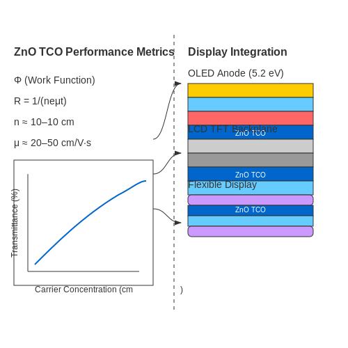
where T is the transmittance (normalized to sheet resistance Rs). Optimized ZnO films achieve ΦTC > 10−2 Ω−1, comparable to ITO but with better bending stability. The carrier concentration (n) and mobility (μ) relationship is critical:
where t is the film thickness. Doped ZnO (e.g., Al:ZnO or Ga:ZnO) achieves n ≈ 1020–1021 cm−3 and μ ≈ 20–50 cm2/V·s through controlled sputtering or atomic layer deposition (ALD).
Integration with Display Architectures
ZnO TCOs are implemented in:
- OLED displays: As anode layers, ZnO’s high work function (~5.2 eV) improves hole injection compared to ITO (~4.7 eV).
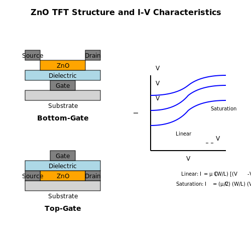
- LCD backplanes: Combined with thin-film transistors (TFTs), ZnO’s high mobility enables faster pixel switching (>1 MHz).
- Flexible electrophoretic displays: ZnO’s fracture strain (≥3%) outperforms ITO (≤1%) under repeated bending.
Challenges and Solutions
Hydrogen diffusion from ZnO into adjacent organic layers in OLEDs can reduce device lifetime. Passivation via SiO2 nanolayers (5–10 nm) mitigates this. For large-area uniformity, pulsed laser deposition (PLD) achieves thickness variations <±2% across Gen 8.5 substrates (2200×2500 mm).
Case Study: Foldable AMOLED
Samsung’s 2023 foldable displays use Ga:ZnO anodes with Rs = 8 Ω/sq at 90% transmittance. The ZnO layer withstands >200,000 folding cycles at 1 mm radius, whereas ITO fails at <20,000 cycles. The improvement arises from ZnO’s polycrystalline structure, which inhibits crack propagation.
5. Stability and Environmental Degradation
5.1 Stability and Environmental Degradation
Chemical Stability Under Ambient Conditions
Zinc oxide (ZnO) transparent conductors exhibit relatively good chemical stability in dry, inert environments due to their wide bandgap (≈3.3 eV) and low intrinsic carrier concentration. However, exposure to moisture, oxygen, and acidic/basic environments can lead to degradation mechanisms:
- Hydrolysis: Water molecules react with ZnO surfaces, forming zinc hydroxide (Zn(OH)2), which increases resistivity.
- Carbonate Formation: Atmospheric CO2 reacts with surface hydroxyl groups, producing insulating zinc carbonate (ZnCO3).
- Photocorrosion: Under UV illumination, electron-hole pairs generated at the ZnO surface participate in redox reactions, accelerating decomposition.
Electrical Degradation Mechanisms
The conductivity of doped ZnO (e.g., Al:ZnO, Ga:ZnO) degrades due to:
where Ea is the activation energy for dopant deactivation, k is Boltzmann's constant, and T is temperature. Primary mechanisms include:
- Oxygen Adsorption: Ambient O2 captures free electrons, reducing carrier concentration.
- Dopant Segregation: Aluminum or gallium dopants migrate to grain boundaries, forming electrically inactive clusters.
- Hydrogen Passivation: Hydrogen atoms diffuse into ZnO, neutralizing dopants by forming Al-H or Ga-H complexes.
Thermal Stability
At elevated temperatures (>200°C), ZnO undergoes structural and electronic changes:
where D is the diffusivity of dopant atoms, Q is activation energy, and R is the gas constant. Key effects include:
- Grain Growth: Increased temperature accelerates crystallite coalescence, reducing scattering at grain boundaries but increasing surface roughness.
- Oxygen Vacancy Annihilation: High-temperature annealing in oxygen-rich atmospheres fills oxygen vacancies, decreasing n-type conductivity.
Mitigation Strategies
To enhance stability, researchers employ:
- Protective Coatings: Thin (<10 nm) layers of SiO2 or Al2O3 deposited via atomic layer deposition (ALD) prevent environmental interactions.
- Alloying: Incorporating magnesium (MgxZn1-xO) increases bandgap and reduces photocorrosion susceptibility.
- Dopant Optimization: Co-doping with hydrogen or fluorine improves thermal stability of carrier concentration.
Accelerated Aging Tests
Standardized environmental tests assess long-term stability:
| Test | Conditions | Degradation Metric |
|---|---|---|
| Damp Heat | 85°C, 85% RH | ΔR/R0 after 1000h |
| Thermal Cycling | -40°C to +85°C | Crack formation density |
| UV Exposure | 1 Sun, AM1.5G | Transmittance loss at 550 nm |
5.2 Scalability and Cost-Effectiveness
Manufacturing Processes and Scale-Up Challenges
The production of zinc oxide (ZnO) transparent conductive oxides (TCOs) primarily relies on two scalable deposition techniques: sputtering and chemical vapor deposition (CVD). Sputtering, particularly radio-frequency (RF) magnetron sputtering, dominates industrial-scale production due to its compatibility with roll-to-roll (R2R) processing. The deposition rate \( R \) in sputtering systems follows:
where \( J \) is the ion current density, \( \eta \) the sputtering yield, \( M \) the molar mass, \( n \) the atomic density, \( e \) the electron charge, and \( \rho \) the material density. For Al-doped ZnO (AZO), typical RF sputtering rates range from 10–50 nm/min at power densities of 2–5 W/cm².
Material and Processing Costs
ZnO-based TCOs exhibit significant cost advantages over indium tin oxide (ITO):
- Raw material costs: Zinc is ~50× cheaper than indium ($$2.5/kg vs. $$150/kg).
- Energy consumption: ZnO sputtering requires 20–30% lower power than ITO due to zinc's lower melting point (1975°C vs. ITO's 2200°C).
- Target utilization: ZnO targets achieve 80–90% material usage versus 60–70% for ITO.
Comparative Cost Analysis
The normalized cost per square meter for 100-nm films breaks down as:
| Material | Target Cost ($$/kg) | Deposition Rate (nm/min) | Power Consumption (kWh/m²) | Total Cost ($$/m²) |
|---|---|---|---|---|
| ITO | 800–1200 | 15–25 | 3.2–4.5 | 12.50–18.75 |
| AZO | 40–60 | 25–50 | 2.1–3.0 | 2.80–4.20 |
Industrial Adoption Barriers
Despite cost advantages, three technical challenges hinder widespread adoption:
- Environmental stability: ZnO degrades in humid environments (RH > 60%) due to hydroxyl group adsorption, increasing resistivity by 10²–10³×.
- Contact resistance: ZnO/metal interfaces exhibit higher Schottky barriers (0.3–0.5 eV) than ITO, requiring additional interfacial layers.
- Uniformity control: Doping homogeneity becomes challenging at deposition rates > 50 nm/min, causing resistivity variations > ±15% across substrates.
Stability Enhancement Strategies
Atomic layer deposition (ALD) of 2–5 nm Al₂O₃ encapsulation layers reduces moisture penetration by 3 orders of magnitude, as described by the diffusion coefficient:
where \( D_0 \) = 5×10⁻⁶ cm²/s for uncoated ZnO versus 2×10⁻⁹ cm²/s for ALD-coated samples at 85°C/85% RH.
5.3 Emerging Research Trends
Doping Strategies for Enhanced Conductivity
Recent advances in doping techniques have significantly improved the conductivity of zinc oxide (ZnO) transparent conductors. Aluminum (Al), gallium (Ga), and indium (In) remain the most studied dopants, but novel co-doping approaches are gaining traction. For instance, dual doping with Al and Ga reduces lattice distortion compared to single-element doping, as described by the defect equilibrium:
First-principles calculations suggest that co-doping with hydrogen (H) further passivates oxygen vacancies, enhancing carrier mobility. Experimental results show resistivities as low as 2×10⁻⁴ Ω·cm for ZnO:Al,H thin films deposited by pulsed laser deposition (PLD).
Nanostructured ZnO for Flexible Electronics
Nanowire and nanoparticle-based ZnO transparent conductors exhibit superior mechanical flexibility compared to conventional thin films. The piezotronic effect in ZnO nanowires enables strain-sensitive conductivity tuning, with applications in foldable displays and wearable sensors. A recent study demonstrated a 90% transmittance and sheet resistance of 15 Ω/sq for silver nanowire-reinforced ZnO meshes.
Hybrid Organic-ZnO Transparent Electrodes
Combining ZnO with conductive polymers like PEDOT:PSS creates hybrid electrodes with work-function tunability. The interfacial energy alignment follows:
Recent work achieved 85% transmittance and sheet resistance below 50 Ω/sq using ZnO/PEDOT:PSS bilayers, with improved environmental stability against humidity degradation.
Ultra-Thin ZnO for Quantum Confinement Effects
Sub-10nm ZnO layers exhibit quantum confinement, altering their optoelectronic properties. The bandgap widening follows the Brus equation:
where R is the nanoparticle radius. This effect enables bandgap tuning from 3.3 eV to 4.0 eV, useful for UV-selective transparent electrodes.
Plasmonic Enhancement with Metallic Nanoparticles
Embedding silver or gold nanoparticles in ZnO matrices creates localized surface plasmon resonances (LSPRs). The scattering cross-section enhancement follows:
where α is the polarizability. This approach boosts near-infrared transmittance while maintaining visible-range conductivity, ideal for tandem solar cells.
6. Key Research Papers
6.1 Key Research Papers
- Transparent Oxide Electronics - Wiley Online Library — 2.1.1 Binary Compounds: the Examples of Zinc Oxide and Indium Oxide 9 2.1.2 Ternary and Quaternary Compounds: the Examples of Indium-Zinc Oxide and Gallium-Indium-Zinc Oxide 12 2.2 Sputtered n-TSOs: Gallium-Indium-Zinc Oxide System 16 2.2.1 Dependence of the Growth Rate on Oxygen Content in the Ar+O 2 Mixture and Target Composition 16
- Transparent Electronics: From Synthesis to Applications — 8 Application of Transparent Amorphous Oxide Thin Film Transistors to Electronic Paper 213 Manabu Ito 8.1 Introduction 213 8.2 Microencapsulated Electrophoretic Display 215 8.3 Flexible Electronic Paper 218 8.3.1 Flexible Display 218 8.3.2 Flexible Electronic Paper Driven by an a-IGZO TFTArray 219 8.4 Application of Transparent Electronics 221
- P-type zinc oxide spinels: application to transparent conductors and ... — Ternary oxides, particularly doped films and compounds of oxides of tin, indium and zinc, have long been known to possess strong transparent conducting properties (Chopra et al 1983).Depending on the components in the compounds, ternary oxides may also exhibit magnetic properties (Kaur et al 2013, 2014, ) and find use as dilute magnetic semiconductors (DMSs) in spintronics (Prinz 1998).
- Transparent Conductive Zinc Oxide | Request PDF - ResearchGate — In 1960, the good piezoelectric properties of zinc oxide were discovered [2], which led to the first electronic application of zinc oxide as a thin layer for surface acoustic wave devices [3 ...
- Fundamentals of zinc oxide as a semiconductor - IOPscience — Rep. Prog. Phys. 72 (2009) 126501 A Janotti andCGVandeWalle A L Γ A H Γ-8-6-4-2 0 2 4 6 8 10 Energy (eV) K Zn O a c [0001] (a) (b) M Figure 1. The wurtzite crystal structure of ZnO with the lattice parameters a and c indicated in (a), and the calculated band structure of ZnO using the HSE hybrid functional in (b).The energy of the valence-band maximum (VBM) was set to zero.
- An overview of recent progress in the development of flexible ... — Contrastly, the utilization of Ag NWs is promising for PI-based flexible transparent conductors, due to the ease of synthesis of Ag NWs and excellent electrical conductivity of Ag NWs. In 2015, Huang et al. fabricated flexible transparent conductors via coating composite aluminum-doped zinc oxide (AZO)-AgNWs conductive layer onto PI substrate [31].
- PDF Materials for Transparent Electrodes: From Metal Oxides to Organic ... — Keywords: Transparent Conductors, Composite Materials, Conducting Polymers, Nanostructures, Flexible Electronics Abstract Nowadays, opto-electronic devices, su ch as displays, are omnipresen t in our daily life. A crucial component of these devices is a transparent elec trode, which allows the in- and out-coupling of light.
- Study of Gallium-Doped Zinc Oxide Thin Films Processed by Atomic Layer ... — Gallium-doped zinc oxide (GZO) films were fabricated using RF magnetron sputtering and atomic layer deposition (ALD). The latter ones demonstrate higher electrical conductivities (up to 2700 S cm-1) and enhanced charge mobilities (18 cm2 V-1 s-1). The morphological analysis reveals differences mostly due to the very different nature of the deposition processes. The film deposited via ALD ...
- Far-infrared transparent conductors | Light: Science & Applications — Transparent conductor (TC) refers to materials with high transmittance and high conductivity in the interesting band 1,2,3.They are widely used as key materials in optoelectronic devices ...
- Computational Prediction and Experimental Realization of Earth-Abundant ... — Transparent conducting oxides (TCOs) are an essential component of modern photovoltaic and display screen technologies. Thin-film Sn-doped In 2 O 3 (ITO) displays the superior optoelectronic properties among the industrially used TCOs; it has been reported to possess resistivities as low as 8 × 10 -5 Ω·cm, mobilities that exceed 50 cm 2 V -1 s -1, and carrier concentrations on the ...
6.2 Books and Review Articles
- PDF Review of flexible and transparent thin-film transistors based on zinc ... — Flexible and transparent electronics presents a new era of electronic technologies. Ubiquitous applications involve wearable electronics, biosensors, flexible transparent displays, radio-frequency identifications (RFIDs), etc.Zinc oxide (ZnO) and related materials are the most commonly used inorganic semiconductors in flexible and transparent devices, owing to their high electrical performance ...
- Critical Review on SnO2 for Transparent Conductor and Electron ... — This article attempts to review the state of the art of synthesis and properties of SnO 2 , focusing primarily on its application as a transparent conductive oxide (TCO) in various optoelectronic devices and second in energy harvesting and energy storage devices where it finds its use as an electron transport layer (ETL) and an electrode ...
- Transparent Oxide Electronics: From Materials to Devices — Transparent electronics is emerging as one of the most promising technologies for the next generation of electronic products, away from the traditional silicon technology. It is essential for touch display panels, solar cells, LEDs and antistatic coatings. The book describes the concept of transparent electronics, passive and active oxide semiconductors, multicomponent dielectrics and their ...
- P-type zinc oxide spinels: application to transparent conductors and ... — The compound is, however, more optically absorbent than generally desirable for transparent electronics. In this work, we look at yet-to-be synthesized first-row transition metal zinc oxide spinels, and compare their electrical transport and optical properties to those of the recently characterized ZnCo O (Perkins et al 2011).
- Oxygen-Doped Zinc Nitride as a High-Mobility Nitride-Based ... — While many types of transparent conducting oxides (TCOs) have been developed, nitride-based transparent conductors remain rare. We examined the properties of zinc nitride doped with oxygen (Zn3N2-xOx) as a potential nitride-based transparent conductor. Electron density on the order of 1020 cm-3 was achieved by heavy oxygen doping. A minimal resistivity (ρ) of 6.2 × 10⁻⁴ Ω cm ...
- Zinc Oxide: The Versatile Material with an Assortment of Physical ... — The lack of transparent p -type oxide material has always been a major obstacle to the fabrication of oxide-based p - n homo and heterojunction devices. Zinc oxide (ZnO) is a II-VI transparent conducting oxide touted as a material of choice for short wavelength optoelectronics.
- PDF Springer Series in MATERIALS SCIENCE 119 — Properties and Applications By F. Poli, A. Cucinotta, and S. Selleri 103 Polarons in Advanced Materials Editor: A.S. Alexandrov 104 Transparent Conductive Zinc Oxide Basics and Applications in Thin Film Solar Cells Editors: K. Ellmer, A. Klein, and B. Rech 105 Dilute III-V Nitride Semiconductors and Material Systems Physics and Technology ...
- Transparent Oxide Electronics - Wiley Online Library — This book provides an overview of the world of transparent electronics, chiefly the processing of oxide semiconductors and their application to transparent TFTs, being essentially focused on the work developed over recent years in our laboratory.
- ZnO‐Based Transparent Conductive Thin Films: Doping, Performance, and ... — ZnO-based transparent conductive thin films have attracted much attention as a promising substitute material to the currently used indium-tin-oxide thin films in transparent electrode applications. However, the detailed function of the dopants, acting on the electrical and optical properties of ZnO-based transparent conductive thin films, is not clear yet, which has limited the development and ...
- PDF Study of Charge Transport Through Zinc Oxide Nanowire Networks for ... — Introduction to transparent conducting thin films 1.1 Indium tin oxide transparent conducting electrodes in modern opto-electronic
6.3 Online Resources and Databases
- Transparent Oxide Electronics - Wiley Online Library — 2.3 Sputtered n-TSOs: Gallium-Zinc-Tin Oxide System 49 2.4 Solution-Processed n-TSOs 51 2.4.1 ZTO by Spray-pyrolysis 51 2.4.2 ZTO by Sol-gel Spin-coating 52 2.4.3 GIZO Sol-gel by Spin-coating 52 References 55 3 P-type Transparent Conductors and Semiconductors 63 3.1 Introduction 63 3.2 P-type Transparent Conductive Oxides 64
- P-type zinc oxide spinels: application to transparent conductors and ... — Ternary oxides, particularly doped films and compounds of oxides of tin, indium and zinc, have long been known to possess strong transparent conducting properties (Chopra et al 1983).Depending on the components in the compounds, ternary oxides may also exhibit magnetic properties (Kaur et al 2013, 2014, ) and find use as dilute magnetic semiconductors (DMSs) in spintronics (Prinz 1998).
- Zinc Oxide Materials for Electronic and ... - Wiley Online Library — Zinc oxide materials for electronic and optoelectronic device applications / edited by Cole W. Litton, Donald C. Reynolds, Thomas C. Collins. p. cm. — (Wiley series in materials for electronic & optoelectronic applications ; 35) Includes bibliographical references and index. ISBN 978--470-51971-4 (hardback) 1. Zinc oxide. 2.
- Transparent Electronics: From Synthesis to Applications — 8 Application of Transparent Amorphous Oxide Thin Film Transistors to Electronic Paper 213 Manabu Ito 8.1 Introduction 213 8.2 Microencapsulated Electrophoretic Display 215 8.3 Flexible Electronic Paper 218 8.3.1 Flexible Display 218 8.3.2 Flexible Electronic Paper Driven by an a-IGZO TFTArray 219 8.4 Application of Transparent Electronics 221
- Zinc oxide [electronic resource] : fundamentals, materials and device ... — Stanford Libraries' official online search tool for books, media, journals, databases, government documents and ... Zinc oxide [electronic resource] : fundamentals, materials and device technology. Responsibility Hadis Morkoç and Ümit Özgür. Imprint Weinheim : Wiley-VCH, c2009. Physical description 1 online resource (xi, 477 p.) : ill. Online.
- Transparent Oxide Electronics: From Materials to Devices — Transparent electronics is emerging as one of the most promising technologies for the next generation of electronic products, away from the traditional silicon technology. It is essential for touch display panels, solar cells, LEDs and antistatic coatings. The book describes the concept of transparent electronics, passive and active oxide semiconductors, multicomponent dielectrics and their ...
- Transparent oxide electronics [electronic resource] : from materials to ... — Stanford Libraries' official online search tool for books, media, journals, databases, government documents and more. Transparent oxide electronics [electronic resource] : from materials to devices in SearchWorks catalog
- PDF Fundamentals of zinc oxide as a semiconductor - University of Chicago — Rep. Prog. Phys. 72 (2009) 126501 A Janotti andCGVandeWalle A L Γ A H Γ-8-6-4-2 0 2 4 6 8 10 Energy (eV) K Zn O a c [0001] (a) (b) M Figure 1. The wurtzite crystal structure of ZnO with the lattice parameters a and c indicated in (a), and the calculated band structure of ZnO using the HSE hybrid functional in (b).The energy of the valence-band maximum (VBM) was set to zero.
- Electronic Properties of Post-transition Metal Oxide Semiconductor ... — The post-transition metal oxides (PTMOs) have traditionally been classified as transparent conductors. The normally contradictory properties of transparency to visible light and electrical conductivity have made materials such as Sn-doped In 2 O 3 and Al-doped ZnO suitable for use as transparent electrodes in devices such as solar cells and flat panel displays.
- PDF Study of Charge Transport Through Zinc Oxide Nanowire Networks for ... — the time to find a suitable alternative low cost transparent conductor that can replace ITO in transparent conducting electrodes. ZnO is a wide band gap semiconducting oxide (Eg ~ 3.4eV) that has the potential to replace ITO as a cheap and flexible transparent electrode material. ZnO nanowires