Solar Inverter Circuits
1. Basic Principles of Solar Inverters
Basic Principles of Solar Inverters
Fundamental Operation
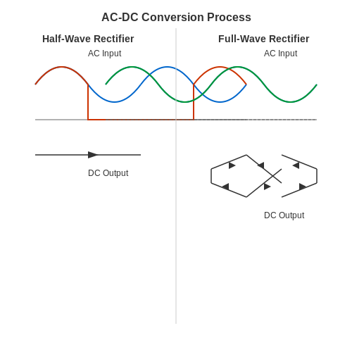
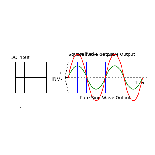
A solar inverter performs the essential function of converting direct current (DC) from photovoltaic (PV) panels into alternating current (AC) suitable for grid connection or local loads. The conversion process involves two key stages: DC-to-AC inversion and synchronization with the grid's voltage and frequency. The core challenge lies in maintaining high efficiency while ensuring the output waveform meets stringent harmonic distortion standards (typically THD < 3% for grid-tied systems).
Topology and Switching Mechanisms
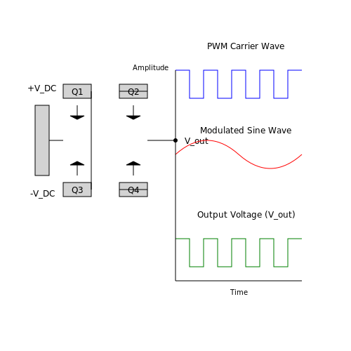
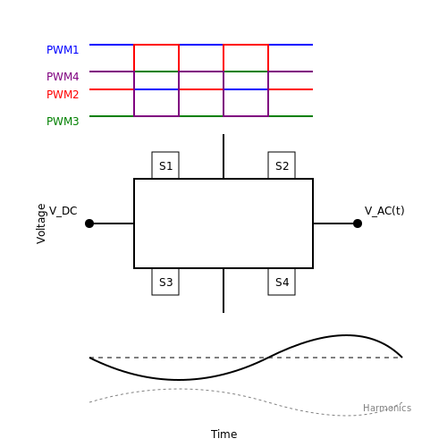
Modern solar inverters predominantly use pulse-width modulation (PWM) controlled H-bridge configurations for the inversion process. The basic single-phase full-bridge inverter consists of four power switches (typically IGBTs or MOSFETs) arranged in two complementary pairs (Q1-Q4 and Q2-Q3). When Q1-Q4 conduct simultaneously, the output voltage is +VDC, while Q2-Q3 conduction produces -VDC.
This Fourier series representation shows the fundamental and harmonic components of the square wave output before filtering. Practical implementations use sinusoidal PWM to approximate a pure sine wave by varying the duty cycle of the switches at high frequency (typically 16-20 kHz).
Maximum Power Point Tracking (MPPT)
An essential subsystem in solar inverters is the MPPT algorithm, which dynamically adjusts the operating point of the PV array to extract maximum available power. The perturb-and-observe (P&O) method remains widely used due to its simplicity:
- Measure array voltage (V) and current (I)
- Calculate power P = V × I
- Apply small perturbation to voltage
- Observe power change direction
- Adjust operating point accordingly
Grid Synchronization
For grid-tied inverters, phase-locked loops (PLLs) precisely synchronize the inverter output with the grid voltage. The PLL adjusts the inverter's phase angle θ until the quadrature component Vq becomes zero:
Advanced implementations use dq0 transformation to decouple active and reactive power control in the rotating reference frame.
Efficiency Considerations
Inverter efficiency η is characterized by two components:
- European efficiency: Weighted average across load levels (ηEU = 0.03η5% + 0.06η10% + ... + 0.5η100%)
- CEC efficiency: California Energy Commission's weighted formula emphasizing mid-range performance
Modern silicon carbide (SiC) MOSFETs have pushed peak efficiencies above 99% by reducing switching losses at high frequencies.
Protection Mechanisms
Critical protection features include:
| Protection Type | Trigger Condition | Response |
|---|---|---|
| Anti-islanding | Grid voltage/frequency deviation | Disconnect within 2 seconds |
| DC injection | DC component > 0.5% of rated current | Shutdown |
| Over-temperature | Heat sink > 85°C | Derate or disconnect |
1.2 Types of Solar Inverters: Grid-Tied, Off-Grid, and Hybrid
Grid-Tied Solar Inverters
Grid-tied inverters synchronize with the utility grid, converting DC power from solar panels into AC power that matches the grid's voltage, frequency, and phase. These inverters employ maximum power point tracking (MPPT) to optimize energy harvest. A critical feature is their ability to disconnect from the grid during outages (anti-islanding protection) to prevent backfeeding, as mandated by IEEE 1547 and UL 1741 standards.
The output power of a grid-tied inverter is given by:
where η is the inverter efficiency (typically 95-98%) and PDC is the DC input power. Modern grid-tied inverters often incorporate reactive power control (Q-V droop) for grid support functions.
Off-Grid Solar Inverters
Off-grid inverters operate independently from the utility grid, typically in systems with battery storage. These inverters must handle variable input voltages from batteries (e.g., 12V-48V DC) while maintaining stable AC output. Key design considerations include:
- Low-voltage disconnect (LVD) to protect batteries
- High surge capacity for motor loads (5-10x rated power)
- Pure sine wave output (THD < 3%)
The battery sizing equation for off-grid systems is:
where Eload is daily energy demand, Dautonomy is days of autonomy, and DODmax is maximum depth of discharge.
Hybrid Solar Inverters
Hybrid inverters combine features of both grid-tied and off-grid systems, with bidirectional power flow capability. Advanced models implement:
- DC-coupled battery integration (higher efficiency than AC-coupled)
- Seamless transfer switching (<10ms)
- Predictive energy management algorithms
The power flow in a hybrid system follows:
where positive Pgrid indicates grid import and negative values indicate export. Modern hybrid inverters often incorporate volt-var and frequency-watt responses for advanced grid interaction.
Comparative Analysis
The table below summarizes key parameters for each inverter type:
| Parameter | Grid-Tied | Off-Grid | Hybrid |
|---|---|---|---|
| Grid Interaction | Required | None | Optional |
| Battery Support | No | Required | Optional |
| Efficiency Range | 96-98% | 90-95% | 94-97% |
| Cost (per kW) | $$0.15-$$0.30 | $$0.50-$$1.00 | $$0.40-$$0.80 |
Emerging topologies like modular multilevel converters (MMC) are pushing efficiency boundaries beyond 99% in commercial-scale implementations, particularly in three-phase systems above 100kW.
Key Components in Solar Inverter Circuits
Power Semiconductor Devices
The core of any solar inverter circuit lies in its power semiconductor devices, which facilitate the conversion of DC to AC. The most commonly used devices include:
- MOSFETs (Metal-Oxide-Semiconductor Field-Effect Transistors): Preferred for high-frequency switching applications due to their fast switching speeds and low gate drive power. The on-resistance RDS(on) is a critical parameter affecting conduction losses.
- IGBTs (Insulated-Gate Bipolar Transistors): Combine the high input impedance of MOSFETs with the low conduction losses of bipolar junction transistors (BJTs). Suitable for high-voltage and high-current applications, typically above 600V.
- SiC (Silicon Carbide) and GaN (Gallium Nitride) Devices: Emerging technologies offering superior performance in terms of thermal conductivity, breakdown voltage, and switching efficiency compared to traditional silicon-based devices.
DC-DC Boost Converter
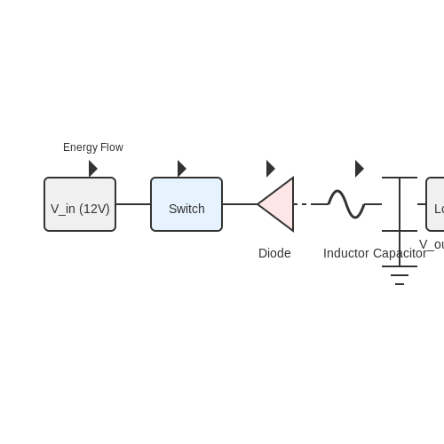
Solar panels often produce variable DC voltages depending on irradiance and temperature. A DC-DC boost converter is employed to step up the voltage to a level suitable for inversion. The converter operates by controlling the duty cycle D of the switching device:
where Vin is the input voltage from the solar panel and Vout is the boosted DC voltage. The inductor and capacitor values are selected based on the desired ripple current and voltage:
where ΔIL is the inductor current ripple, ΔVout is the output voltage ripple, and fsw is the switching frequency.
H-Bridge Inverter
The H-bridge configuration is the standard topology for converting DC to AC. It consists of four switches (typically IGBTs or MOSFETs) arranged in an "H" pattern. By alternately switching the pairs (S1-S4 and S2-S3), a square wave or modified sine wave is generated. For pure sine wave output, Pulse Width Modulation (PWM) techniques are applied:
where VDC is the input DC voltage, ω is the angular frequency, and n represents the harmonic components.
Filter Components
To attenuate high-frequency harmonics and produce a clean sinusoidal output, LC or LCL filters are employed. The cutoff frequency fc of an LC filter is given by:
For grid-tied inverters, LCL filters are preferred due to their superior harmonic suppression. The design must ensure that the resonant frequency fres lies outside the inverter's operating range to avoid instability:
Maximum Power Point Tracking (MPPT) Controller
An MPPT controller optimizes the power extraction from the solar panel by dynamically adjusting the operating point. The Perturb and Observe (P&O) algorithm is widely used due to its simplicity:
- Measure panel voltage V and current I.
- Calculate power P = V × I.
- Perturb the voltage slightly and observe the change in power.
- Adjust the voltage in the direction of increasing power.
For higher precision, incremental conductance methods are employed, leveraging the derivative of the power-voltage curve:
Isolation and Protection Circuits
Galvanic isolation is critical for safety and noise immunity. High-frequency transformers or optocouplers are used to isolate control signals from power stages. Overcurrent and overvoltage protection circuits, often incorporating fast-acting fuses and varistors, safeguard the inverter from transient surges.
2. Circuit Topologies for Solar Inverters
2.1 Circuit Topologies for Solar Inverters
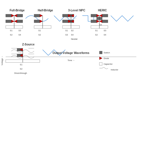
Full-Bridge Inverter
The full-bridge (H-bridge) inverter is the most widely used topology for solar applications due to its ability to generate pure sinusoidal output with high efficiency. It consists of four switching devices (typically IGBTs or MOSFETs) arranged in two legs. The output voltage Vout is synthesized by pulse-width modulation (PWM) of the switches:
where DA and DB are duty cycles of the upper switches in each leg. Dead-time insertion is critical to prevent shoot-through currents, typically implemented in the range of 100–500 ns.
Half-Bridge Inverter
For lower-power applications (< 1 kW), a half-bridge configuration reduces component count at the cost of requiring a split DC link. The output voltage swings between +Vdc/2 and -Vdc/2, with the neutral point stabilized by large electrolytic capacitors. The fundamental output voltage is given by:
where ma is the modulation index (0 ≤ ma ≤ 1). This topology exhibits higher total harmonic distortion (THD) compared to full-bridge designs.
Multilevel Inverters
For grid-scale solar plants (> 100 kW), multilevel topologies like the Neutral-Point Clamped (NPC) or Cascaded H-Bridge (CHB) reduce dv/dt stress and improve harmonic performance. A 3-level NPC inverter produces output voltages in three states (+Vdc/2, 0, -Vdc/2), with the switching function:
where x denotes the phase leg. The NPC topology reduces switch voltage ratings to half of the DC bus voltage.
Transformerless Topologies
Transformerless designs like the HERIC (Highly Efficient and Reliable Inverter Concept) eliminate the 60 Hz transformer, achieving >98% efficiency. Leakage current suppression is achieved through decoupling networks, with the common-mode voltage VCM held constant:
This requires symmetric PWM patterns and careful PCB layout to minimize parasitic capacitances to ground.
Z-Source Inverter
The Z-source topology integrates impedance networks to provide voltage buck-boost capability, overcoming the limitation of conventional inverters where Vac must be less than Vdc. The boost factor B is determined by the shoot-through duty ratio DST:
This allows MPPT operation over wider PV voltage ranges without requiring a separate DC-DC stage.
2.2 Pulse Width Modulation (PWM) Techniques
Fundamentals of PWM in Inverter Circuits
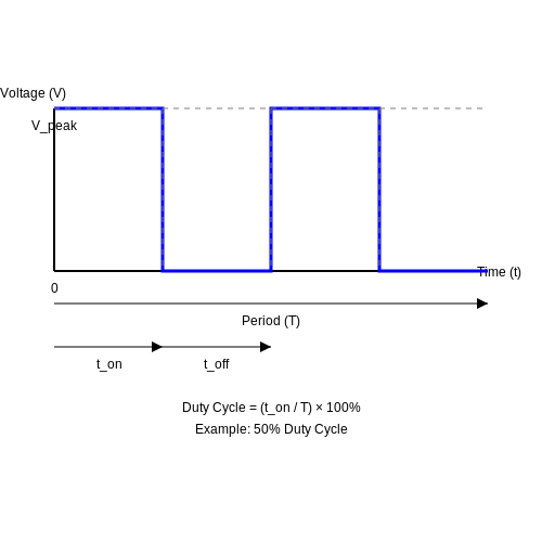
Pulse Width Modulation (PWM) is a switching technique used to control the average power delivered to a load by rapidly switching a voltage source on and off. The key parameter is the duty cycle (D), defined as the ratio of the pulse duration (ton) to the total period (T):
In solar inverters, PWM regulates the output voltage or current by adjusting D while maintaining a fixed switching frequency (fsw). The output voltage (Vout) of an inverter with DC input VDC is:
Carrier-Based PWM
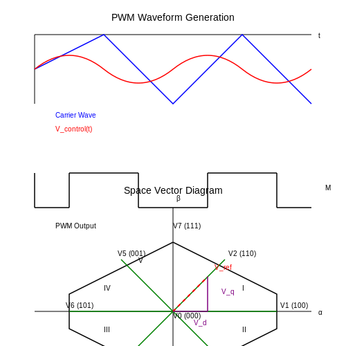
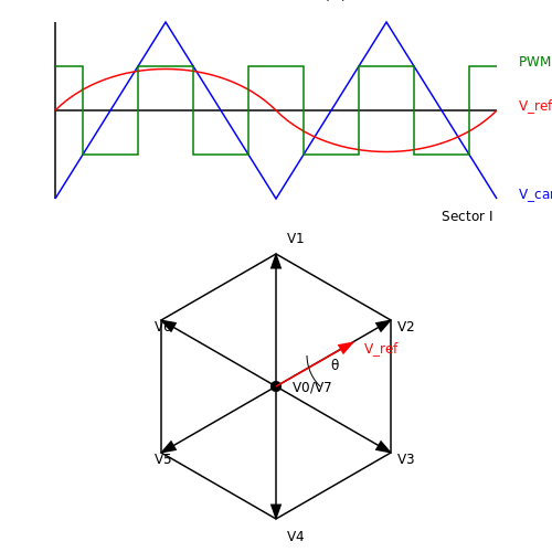
Most solar inverters use sinusoidal PWM (SPWM), where a high-frequency triangular carrier wave (Vcarrier) is compared to a sinusoidal reference signal (Vref). The intersection points determine the switching instants:
where M is the modulation index (0 ≤ M ≤ 1) and fm is the fundamental frequency. The output harmonics are concentrated around multiples of fsw, simplifying filtering.
Space Vector PWM (SVPWM)
For three-phase inverters, SVPWM offers superior DC-link utilization (15.5% higher than SPWM) by synthesizing the output voltage as a combination of eight discrete switching vectors. The reference vector (Vref) is approximated using adjacent active vectors and zero vectors:
where T1, T2 are the durations of active vectors, and T0 is the zero vector duration.
Dead-Time Compensation
Practical implementations require a dead time (td) between complementary switch transitions to prevent shoot-through. This introduces voltage distortion, compensated by:
where iload is the load current direction.
Advanced Techniques
- Third-Harmonic Injection: Increases maximum output voltage to 1.15×DC-link voltage by adding a third harmonic to the reference.
- Discontinuous PWM (DPWM): Reduces switching losses by clamping one phase to positive/negative rail for 60° intervals.
- Predictive PWM: Uses load current feedback to dynamically adjust switching patterns for minimal THD.
Maximum Power Point Tracking (MPPT) in Inverters
Fundamentals of MPPT
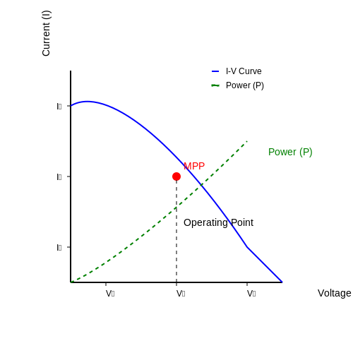
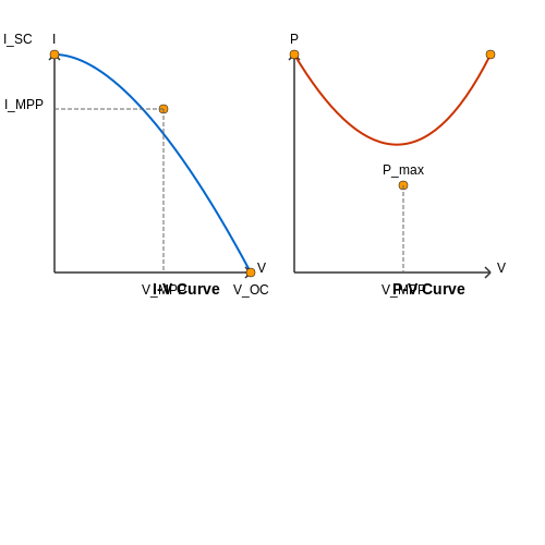
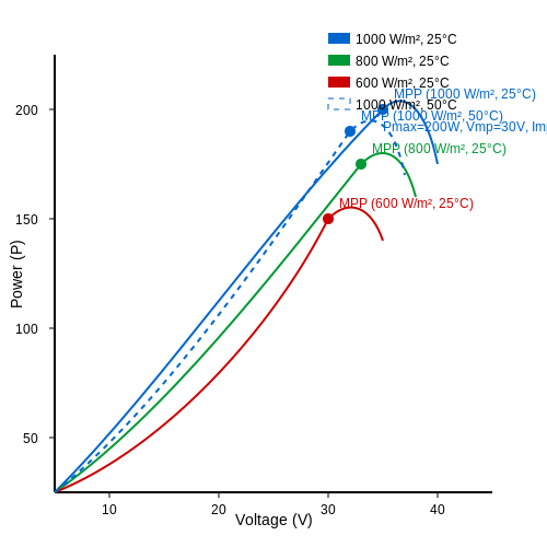
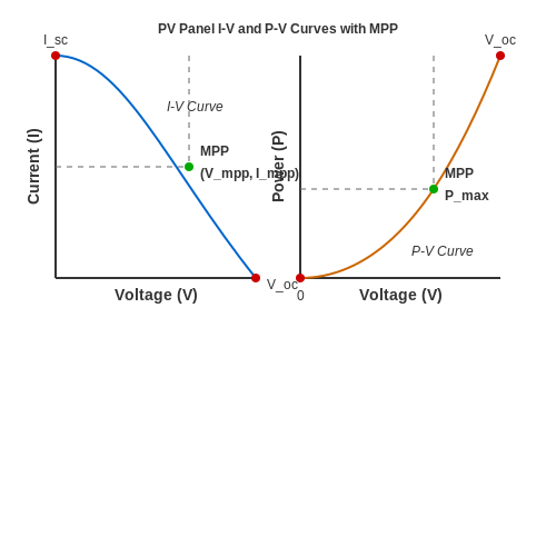
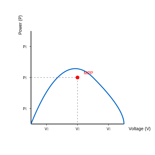
Maximum Power Point Tracking (MPPT) is an essential algorithm in solar inverters designed to extract the maximum available power from photovoltaic (PV) panels under varying environmental conditions. The power-voltage (P-V) characteristic of a solar panel exhibits a nonlinear relationship, with a distinct peak known as the Maximum Power Point (MPP). This point shifts dynamically due to changes in irradiance, temperature, and load conditions.
where \( P_{mp} \) is the maximum power, \( V_{mp} \) is the voltage at MPP, and \( I_{mp} \) is the current at MPP. The MPPT algorithm continuously adjusts the operating point of the inverter to track this peak.
MPPT Techniques
Several MPPT techniques exist, each with trade-offs in convergence speed, accuracy, and implementation complexity:
- Perturb and Observe (P&O): A widely used method that perturbs the operating voltage and observes the resulting power change. If power increases, the perturbation continues in the same direction; otherwise, it reverses.
- Incremental Conductance (IncCond): Based on the principle that the derivative of power with respect to voltage (\( dP/dV \)) is zero at MPP. It offers higher accuracy than P&O under rapidly changing conditions.
- Fractional Open-Circuit Voltage (FOCV): Approximates MPP as a fixed fraction (typically 0.7–0.8) of the open-circuit voltage (\( V_{oc} \)). Simple but less accurate under partial shading.
- Neural Networks and AI-Based Methods: Utilize machine learning to predict MPP under complex conditions, improving adaptability but requiring significant computational resources.
Mathematical Derivation of MPPT Efficiency
The efficiency of an MPPT algorithm is defined as the ratio of the actual harvested power to the theoretically available maximum power:
For the P&O method, the steady-state oscillation around MPP can be minimized by optimizing the perturbation step size (\( \Delta V \)). The power loss due to oscillation is given by:
where \( R_{MPP} = V_{mp}/I_{mp} \) is the equivalent resistance at MPP.
Hardware Implementation
MPPT is typically implemented using a DC-DC converter (boost, buck, or buck-boost) controlled by a microcontroller or dedicated MPPT IC. The converter adjusts its duty cycle (\( D \)) to vary the effective load impedance seen by the PV panel, forcing operation at MPP. For a boost converter:
where \( V_{in} \) is the panel voltage and \( V_{out} \) is the inverter input voltage. The duty cycle is dynamically adjusted based on the MPPT algorithm's output.
Challenges and Practical Considerations
- Partial Shading: Causes multiple local maxima in the P-V curve, complicating MPPT. Global MPPT techniques (e.g., sweep-based methods) are required.
- Fast Transient Response: Rapid changes in irradiance (e.g., passing clouds) demand high sampling rates and adaptive step sizes.
- Converter Losses: Switching and conduction losses in the DC-DC converter reduce overall efficiency, necessitating high-efficiency topologies like synchronous rectification.
Case Study: MPPT in Grid-Tied Inverters
In grid-tied systems, the inverter must synchronize MPPT with grid requirements. Advanced inverters use dual-stage conversion: a DC-DC stage for MPPT followed by a DC-AC stage for grid synchronization. Real-world data from a 5 kW system shows MPPT efficiency exceeding 98% under stable conditions but dropping to ~92% during partial shading.
3. Step-by-Step Guide to Building a Basic Solar Inverter
Step-by-Step Guide to Building a Basic Solar Inverter
Circuit Topology and Operating Principle
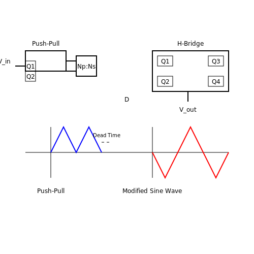
A basic solar inverter converts DC power from photovoltaic (PV) panels into AC power suitable for grid-tied or off-grid applications. The most common topology for small-scale inverters is the push-pull converter followed by an H-bridge for generating a modified sine wave. The push-pull stage boosts the low PV voltage (12-48V) to a higher DC bus voltage (170-400V), while the H-bridge inverts this to AC (110V/220V, 50Hz/60Hz).
The operating principle relies on high-frequency switching (20-100kHz) in the push-pull stage and line-frequency switching (50/60Hz) in the H-bridge. This two-stage approach improves efficiency compared to single-stage designs by allowing separate optimization of the boost and inversion processes.
Key Components and Design Equations
1. Push-Pull Converter
The push-pull converter uses a center-tapped transformer with two primary switches (MOSFETs or IGBTs). The duty cycle D determines the voltage conversion ratio:
where Ns/Np is the secondary-to-primary turns ratio. For stable operation, the maximum duty cycle should not exceed 45% to prevent core saturation.
2. H-Bridge Inverter
The H-bridge generates AC by alternately switching diagonal transistor pairs (Q1/Q4 and Q2/Q3) at the desired output frequency. The RMS output voltage is:
For a modified sine wave with peak voltage Vp, this simplifies to:
Practical Implementation Steps
1. Transformer Design
Select a ferrite core with sufficient power handling capacity. The primary inductance Lp must satisfy:
where ΔI is the allowable current ripple (typically 20-30% of peak current) and fsw is the switching frequency.
2. Switching Devices
MOSFET selection criteria include:
- Voltage rating ≥ 2 × maximum DC bus voltage
- Current rating ≥ 3 × average input current
- Low RDS(on) (< 100mΩ for < 1kW designs)
3. Control Circuitry
A microcontroller or dedicated PWM IC (e.g., SG3525) generates:
- High-frequency PWM for the push-pull stage (20-100kHz)
- Low-frequency complementary signals for the H-bridge (50/60Hz)
Dead time (typically 1-2μs) must be inserted between complementary signals to prevent shoot-through.
Protection and Efficiency Optimization
Critical protection features include:
- Overcurrent protection using current sense resistors
- Overvoltage protection with Zener diodes or TVS devices
- Thermal shutdown via NTC thermistors
Efficiency improvements focus on:
- Minimizing switching losses through proper gate drive design
- Reducing conduction losses via proper PCB layout (wide traces, Kelvin connections)
- Optimizing transformer design (Litz wire, proper core material)
Performance Verification
Key measurements include:
- Total harmonic distortion (THD) < 5% for grid-tied applications
- Efficiency > 90% at rated power
- Voltage regulation within ±2% across load variations
The output waveform can be analyzed using:
where Vh is the RMS voltage of harmonic h and V1 is the fundamental component.
3.2 Common Issues and Solutions in Solar Inverter Circuits
Overvoltage and Undervoltage Conditions
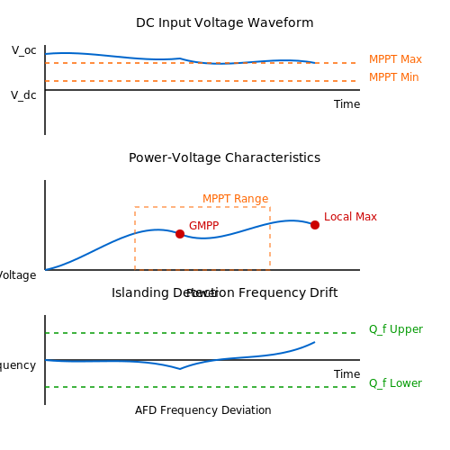
Solar inverters are susceptible to voltage fluctuations caused by varying solar irradiance or grid instability. Overvoltage occurs when the DC input exceeds the inverter's maximum power point tracking (MPPT) range, leading to protective shutdowns or component stress. The voltage at the inverter input can be modeled as:
where Voc is the open-circuit voltage, Ipv is the photovoltaic current, and Rs is the series resistance. Undervoltage, conversely, arises when the input falls below the minimum MPPT threshold, causing inefficient operation. Solutions include:
- Active clamping circuits to suppress voltage spikes.
- Wide-input MPPT algorithms to extend operational range.
- Dynamic DC-link capacitance adjustment to stabilize transient responses.
Islanding and Anti-Islanding Protection
Islanding occurs when the inverter continues supplying power to a local grid segment after mains disconnection, posing safety risks. Anti-islanding techniques detect grid failure through:
- Active frequency drift (AFD): Perturbs the output frequency to force a detectable deviation.
- Impedance measurement: Monitors grid impedance changes during fault conditions.
The detection threshold for islanding can be derived from the quality factor Qf of the local load:
Modern inverters implement IEEE 1547-2018 standards, requiring islanding detection within 2 seconds.
Thermal Management and Component Degradation
Power semiconductors (IGBTs, MOSFETs) in inverters experience thermal cycling, leading to solder joint fatigue or gate oxide degradation. The Arrhenius equation models failure rates:
where Ea is activation energy, k is Boltzmann's constant, and T is junction temperature. Mitigation strategies include:
- Phase-change materials (PCMs) for transient heat absorption.
- Predictive thermal modeling using finite element analysis (FEA).
- SiC/GaN devices for lower conduction losses.
Electromagnetic Interference (EMI)
High-frequency switching generates conducted and radiated EMI, affecting nearby equipment. The spectral density of switching noise is:
where tr is the rise time. Countermeasures involve:
- Common-mode chokes to attenuate high-frequency currents.
- Shielded magnetics with nanocrystalline cores.
- Spread-spectrum modulation to disperse EMI energy.
MPPT Tracking Errors
Partial shading or module mismatch causes multiple maxima in the P-V curve, confusing conventional perturb-and-observe (P&O) algorithms. The global maximum power point (GMPP) can be located using:
Advanced solutions incorporate:
- Machine learning-based MPPT trained on historical irradiance data.
- Distributed power electronics (DPE) with module-level optimizers.
3.3 Safety Considerations and Best Practices
Electrical Isolation and Grounding
Proper electrical isolation is critical in solar inverter circuits to prevent leakage currents and ensure user safety. Galvanic isolation, typically achieved using high-frequency transformers or optocouplers, must withstand the system's maximum voltage with a safety margin. The isolation barrier should comply with IEC 62109-1, which mandates a minimum creepage distance of 8 mm for 300 V systems and 14 mm for 600 V systems. Grounding must follow NEC Article 690.47, ensuring all exposed conductive parts are bonded to the grounding electrode system.
For transformerless inverters, residual current monitoring devices (RCMDs) must detect leakage currents exceeding 30 mA, as per IEC 62477-1. The ground fault protection circuit should interrupt the current within 100 ms at 120% of the rated leakage threshold. The grounding resistance must satisfy:
where \( R_g \) is the grounding resistance and \( I_{\text{leak}} \) is the maximum permissible leakage current (typically 10 mA for residential systems).
Arc Fault Mitigation
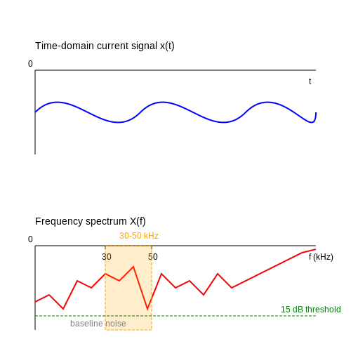
DC arc faults in photovoltaic systems pose fire hazards due to sustained high-current discharges. Series arcs exhibit voltages exceeding 600 V, while parallel arcs generate currents up to the array's short-circuit current \( I_{sc} \). Arc fault circuit interrupters (AFCIs) must detect these anomalies within 2.5 seconds, as specified in UL 1699B. The arc detection algorithm should analyze high-frequency noise components (2-100 kHz) using Fourier transforms:
where \( x(t) \) is the time-domain current signal and \( X(f) \) represents its frequency components. A threshold of 15 dB above baseline noise in the 30-50 kHz band reliably indicates arc formation.
Thermal Management
Power devices (IGBTs, MOSFETs) in inverters experience junction temperature swings that accelerate failure mechanisms. The Arrhenius model predicts lifetime reduction:
where MTTF is mean time to failure, \( E_a \) is activation energy (0.7 eV for silicon devices), and \( T_j \) is junction temperature. Forced air cooling must maintain \( T_j \) below 125°C, with heatsinks sized using thermal resistance calculations:
Place power devices on thermally conductive pads (k ≥ 5 W/mK) and use copper planes (2 oz/ft² minimum) for heat spreading. Temperature sensors should sample at 10 Hz with ±1°C accuracy.
Surge Protection
Lightning-induced surges require coordinated protection across DC and AC sides. The protection strategy follows IEC 61643-31, implementing:
- Class I arrestors (10/350 μs waveform) at service entrance
- Class II arrestors (8/20 μs) at subpanels
- TVS diodes for sensitive electronics
The let-through voltage must remain below 1.5 times the system voltage. For a 600 V DC system, the protection devices should clamp at:
Grounding conductors for surge protection must be shorter than λ/10 at the highest frequency of interest (typically 1 m maximum for 30 MHz components).
Lockout/Tagout Procedures
Maintenance safety requires compliance with OSHA 29 CFR 1910.269. Before servicing, measure residual DC voltage across all capacitors using a Category III-rated multimeter. The discharge circuit must reduce voltages below 50 V within 30 seconds, achieved by:
where \( V_0 \) is the initial capacitor voltage. For a 1000 μF bus capacitor charged to 400 V, the discharge resistor must be:
Use two independent discharge paths (e.g., bleeder resistors + manual discharge tool) for redundancy.
Electromagnetic Compatibility
Inverters must meet CISPR 11 Class A/B emissions limits. Switch-mode frequencies above 150 kHz require careful PCB layout:
- 4-layer stackup with dedicated ground plane
- Keep high di/dt loops (DC link capacitor to switches) under 5 cm²
- Place snubbers within 1 cm of switching devices
Common-mode chokes should attenuate noise by at least 40 dB at the switching frequency. The required inductance is:
where \( Z_0 \) is the line impedance (typically 50 Ω), \( f_{sw} \) is the switching frequency, and A is the desired attenuation in dB.
4. Smart Inverters and IoT Integration
4.1 Smart Inverters and IoT Integration
Architecture of Smart Inverters
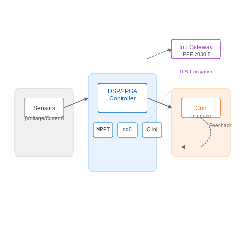
Smart inverters extend traditional grid-tied inverters by incorporating real-time data processing, bidirectional communication, and adaptive control. The core components include:
- DSP/FPGA-based control for high-speed MPPT and grid synchronization.
- IoT gateways (e.g., Wi-Fi, Zigbee, or LoRa) for cloud connectivity.
- Edge-computing modules to preprocess sensor data (voltage, current, temperature) locally.
Communication Protocols and Standards
IoT-enabled inverters adhere to industry standards for interoperability:
- IEEE 2030.5 (Smart Energy Profile 2.0) for demand-response signaling.
- Modbus TCP/RTU for industrial device networking.
- MQTT for lightweight telemetry streaming to cloud platforms like AWS IoT or Azure.
Adaptive Control Algorithms
Smart inverters dynamically adjust operating parameters using feedback from grid conditions and load profiles. The reactive power (Q) injection is governed by:
where X is the grid impedance and Xref is the target reactance. For harmonic compensation, a dq0-transform-based controller minimizes THD:
Cybersecurity Considerations
IoT integration introduces attack surfaces mitigated through:
- TLS 1.3 encryption for data in transit.
- Hardware security modules (HSMs) for key management.
- Anomaly detection via machine learning on power-flow patterns.
Case Study: Virtual Power Plants (VPPs)
In California’s SGIP, 5,000+ smart inverters aggregate into a 50 MW VPP. Each inverter participates in frequency regulation by modulating output power (P) based on grid operator commands:
4.2 Efficiency Optimization Techniques
1. Switching Loss Reduction
Switching losses in power semiconductors (MOSFETs, IGBTs) arise from non-ideal switching transitions and can be modeled as:
where tr and tf are the rise/fall times, and fsw is the switching frequency. Soft-switching techniques like Zero-Voltage Switching (ZVS) and Zero-Current Switching (ZCS) eliminate voltage-current overlap losses by ensuring:
- Transistors turn on only when VDS ≈ 0 (ZVS)
- Transistors turn off only when ID ≈ 0 (ZCS)
2. Conduction Loss Minimization
Conduction losses are governed by the on-state resistance RDS(on) or forward voltage drop VCE(sat):
Optimization strategies include:
- Parallel connection of devices to reduce effective RDS(on)
- Using wide-bandgap semiconductors (SiC/GaN) with lower conduction losses
- Dynamic gate drive voltage adjustment based on load current
3. Maximum Power Point Tracking (MPPT) Algorithms
The perturb-and-observe (P&O) method adjusts the operating voltage to track the MPP where dP/dV = 0. The incremental conductance algorithm improves dynamic response by solving:
Advanced techniques like neural-network-based MPPT achieve >99% tracking efficiency under partial shading conditions.
4. Transformerless Topology Optimization
Eliminating the isolation transformer reduces core losses but introduces leakage current. The H5, HERIC, and oH5 topologies suppress leakage currents by:
- Creating high-frequency common-mode voltage symmetry
- Using active clamping circuits
- Implementing virtual DC buses
The leakage current Ileak in a non-isolated inverter is given by:
where CPV is the panel-to-ground capacitance and VCM is the common-mode voltage.
5. Thermal Management
Junction temperature affects both switching speed and conduction losses. The thermal impedance model:
dictates the need for:
- Phase-change materials for high thermal capacitance
- 3D-printed microchannel heat sinks
- Active cooling with variable-speed fans
6. Harmonic Filtering
Total harmonic distortion (THD) below 5% requires optimized LCL filter design. The resonant frequency must satisfy:
Active harmonic compensation injects counter-phase currents to cancel 3rd, 5th, and 7th harmonics.
4.3 Future Trends in Solar Inverter Technology
Wide-Bandgap Semiconductor Adoption
The shift from silicon (Si) to wide-bandgap (WBG) materials like silicon carbide (SiC) and gallium nitride (GaN) is accelerating due to their superior material properties. These semiconductors exhibit higher breakdown voltages (Ecrit), lower switching losses, and improved thermal conductivity. For instance, SiC MOSFETs reduce conduction losses by up to 50% compared to Si IGBTs at high frequencies. The figure of merit (FOM) for switching performance is given by:
where Ron is on-resistance and Qgd is gate-drain charge. WBG devices achieve FOM values an order of magnitude lower than Si.
Advanced Topologies for Partial Shading Mitigation
Distributed maximum power point tracking (DMPPT) architectures are replacing centralized inverters in utility-scale installations. Submodule-level power optimizers using flyback or buck-boost converters minimize losses under partial shading. A comparative analysis of topologies yields the efficiency (η) improvement:
versus 94–96% for traditional string inverters under mismatch conditions.
AI-Driven Predictive Maintenance
Machine learning models are being deployed for fault anticipation in solar inverters. Long short-term memory (LSTM) networks process time-series data from current/voltage sensors to predict capacitor aging or IGBT degradation. The failure probability Pf is modeled as:
where λ(t) is the hazard function learned from historical failure data. Field tests show a 30% reduction in unscheduled downtime.
Grid-Forming Inverters for Weak Grids
Next-generation inverters are incorporating virtual synchronous machine (VSM) algorithms to provide grid stability without rotational inertia. The swing equation implementation includes synthetic inertia (Jsynth):
where D is the damping coefficient. This enables seamless operation during grid disturbances with less than 2% frequency deviation.
Bidirectional Vehicle-to-Grid (V2G) Integration
Emerging standards like ISO 15118-20 enable solar inverters to interface with electric vehicle batteries. The power flow equation for V2G operation is:
achieving round-trip efficiencies of 92–94% in recent pilot projects.
High-Frequency Transformer Isolation
3–5 MHz resonant converters using planar transformers reduce size by 60% compared to 50/60 Hz designs. The leakage inductance (Llk) and resonant capacitance (Cr) are tuned to achieve zero-voltage switching:
Experimental prototypes demonstrate 97.2% efficiency at 3 kW power levels.
5. Essential Books and Research Papers
5.1 Essential Books and Research Papers
- (PDF) Solar Inverter Project Report - Academia.edu — Thus, for portable AC power, inverters are needed. Inverters take a DC voltage from a battery or a solar panel as input, and convert it into an AC voltage output. FIG 1.4 - SOLAR INVERTER SCHEMATICS 6 1.5 TYPES OF SOLAR INVERTER Solar inverters may be classified into three broad types. 1. Stand Alone Inverters 2. Grid Tie Inverters 3.
- Inverters PDF | PDF | Power Inverter | Power Electronics - Scribd — The document discusses inverters, which convert DC to AC power. It defines inverters and classifies them based on input sources and output phases. Some applications of inverters include solar power systems, motor drives, and UPS devices. Voltage source inverters are analyzed in detail, including full-bridge inverter topology and output voltage waveforms with resistive and inductive loads ...
- A comprehensive review on inverter topologies and control strategies ... — The grid-connected inverters undergone various configurations can be categorized in to four types, the central inverters, the string inverters, the multi-string inverts and the ac module inverters. The four types are shown in Fig. 13 and explained below with their design characteristics, advantages and limitations ( Fig. 14 and 15 ).
- Design and Construction of A 5kva Solar Inverter — Solar power inverter system is consisted of solar panels, charger controllers, inverters and rechargeable batteries, while solar DC power system is not included inverters. Basically, solar power source makes it possible to provide a clean reliable and quality supply of alternative electricity free of surges which could be found in the line ...
- PDF Hybrid Inverter With Solar Battery Charging - Jetir — Figure 3.1 Block diagram of hybrid inverter with solar battery charging 3.1 COMPONENTS 3.1.1 SOLAR PANEL Photo voltaic solar panels absorb sunlight as a source of energy to generate electricity. A photovoltaic (PV) module is a packaged, connect assembly of typically 6x10 photo voltaic solar cells.
- (PDF) Chapter 05: Inverters - Academia.edu — In this research, AC three-level waveform single phase inverter was developed and created by a microcontroller PIC16F627A-I/P with varied maximum voltage angle from 200 to 1800 and tested to a load of 240 V, 20 W AC aquarium water pump, and also analyzed effect of maximum voltage angle on the three-level single phase inverter performance.
- Solar Inverter Equipped with a Battery Management System — This paper presents the results of recent research on the dynamic Li-ion battery management system . ... 2.2 Fundamental of Solar Inverters. A block diagram showing the operation of a solar inverter. Power semiconductors arranged in the best feasible architecture serve as an inverter's brains. ... The primary driver of cost and reliability ...
- DESIGN, SIMULATION & IMPLEMENTATION OF INVERTER - ResearchGate — Multilevel inverters are an emerging area of research in the field of power electronic circuits and applications. It has many advantages like near-sinusoidal output voltage, lower total harmonic ...
- Design and Implementation of a 5 kVA Inverter - ResearchGate — The paper describes the design and construction of a 5 kVA Pulse Width Modulated (PWM) Metal Oxide Semiconductor Field Effect Transistor (MOSFET)-based inverter, which works on the principle of PWM.
- PDF PV Inverter Design Using Solar Explorer Kit (Rev. A) - Texas Instruments — the solar panel, a PV emulator power stage is integrated on the board along with other stages that are needed to process power from the panel. Using a Piccolo-A device integrated on the board lessens the burden of the controller used to control the solar power conditioning circuit control of the PV panel.
5.2 Online Resources and Tutorials
- PDF 'Modular Electronics Learning (ModEL) project' - The Public's Library ... — Modular Electronics Learning (ModEL) project v1 1 0 dc 12 v2 2 1 dc 15 r1 2 3 4700 r2 3 0 7100.end * SPICE ckt ... 2 Case Tutorial 7 2.1 Example: inverter circuits from the Bright/Royer 1957 patent . . . . . . . . . . . . . 8 ... Inverter Circuits" granted 26 February 1957) shows schematic diagrams for several DC-AC inverters. ...
- Inverters PDF | PDF | Power Inverter | Power Electronics - Scribd — The document discusses inverters, which convert DC to AC power. It defines inverters and classifies them based on input sources and output phases. Some applications of inverters include solar power systems, motor drives, and UPS devices. Voltage source inverters are analyzed in detail, including full-bridge inverter topology and output voltage waveforms with resistive and inductive loads ...
- design and construction of a 2.5kva solar inverter — 3.1 Basic designs of a solar inverter. 3.2 block diagram of the system. 3.3 Description of solar inverter units. 3.4 Modified sine wave power solar inverter circuit using ic 4093. 3.5 Circuit operation. 3.6 Description of components used. 3.7 How to choose the best inverter battery
- Design and Construction of A 5kva Solar Inverter — Solar power inverter system is consisted of solar panels, charger controllers, inverters and rechargeable batteries, while solar DC power system is not included inverters. Basically, solar power source makes it possible to provide a clean reliable and quality supply of alternative electricity free of surges which could be found in the line ...
- PDF SUN Inverter Manual - Victron Energy — 2.2. Solar charge controller. The SUN inverter is equipped with a PWM solar regulator. Solar panels can be directly connected to the SUN inverter. Solar power will be used to charge the batteries or help to provide energy to the inverter AC load. The solar charger is fully configurable, for more information see the CHARGE mode [20] chapter. 2.3.
- Design and Implementation of 5kVA Photovoltaic Power System - Academia.edu — Fig 2.10: Low Voltage PWM Inverter Circuit Diagram Figure 2.11: High Voltage PWM Inverter Circuit Diagram 2.6.3 modified sine wave: Figure 2.12: Modified Sine waveform A "modified sine wave" inverter has a non-square waveform that is a useful rough approximation of a sine wave for power translation purposes as shown in Fig. 2.12 below.
- Design and Construction of A 500w Solar Power Inverter — Description. ABSTRACT This work is on design and construction of a 500VA solar power inverter system.. Solar inverter converts the variable direct current (DC) output of a photovoltaic (PV) solar panel into a utility frequency alternating current (AC) that can be fed into a commercial electrical grid or used by a local, off-grid electrical network.
- Inverters - PVEducation — Purpose and Function. Inverters are used to turn the direct current (DC) output of the solar modules into alternating current (AC). This current then flows in the breaker box to be either used in the house or transferred to the electrical grid.. Most appliances and loads within a home use AC current operating at 60 Hz in North America and 50 Hz in most of the rest of the world.
- PDF UNIT V INVERTERS - aec.edu.in — The word 'inverter' in the context of power-electronics denotes a class of power conversion (or power conditioning) circuits that operates from a dc voltage source or a dc current source and converts it into ac voltage or current. The inverter does reverse of what ac-to-dc converter does (refer to ac to dc converters).
- PDF PV Inverter Design Using Solar Explorer Kit (Rev. A) - Texas Instruments — the solar panel, a PV emulator power stage is integrated on the board along with other stages that are needed to process power from the panel. Using a Piccolo-A device integrated on the board lessens the burden of the controller used to control the solar power conditioning circuit control of the PV panel.
5.3 Industry Standards and Certification Guidelines
- PDF IEEE 1547 Overview - Energy.gov — 4 Content ¾Background ¾IEEE Standards ¾1547 Series of Standards • ANSI/IEEE Std 1547 (2003): Standard for interconnection system & interconnection test requirements for interconnecting DR with Electric Power Systems (EPS) • P1547.1 Standard for interconnection test procedures • P1547.2 Guide to 1547 standard • P1547.3 Guide for information exchange for DR
- PDF Standards for the assessment of the environmental performance of ... — solar photovoltaic (PV) modules, inverters and systems, this report aims to: Identify, describe and compare existing standards and new standards under development, relevant to energy performance, reliability, degradation and lifetime. Identify aspects not covered by existing standards, for which transitional methods
- PDF International Guideline for the Certification of Photovoltaic - IEA-PVPS — standards or international standards to be written This report is a summary of the topic "Testing and Certification Methods" for the Subject 51.3, "Reporting of Photovoltaic System Grid-interconnection Technology". The report is generic in format and is intended to provide an overview international guideline for the
- PDF The Solar PV Standard - MCS — Working with industry we define, maintain and improve quality certifying products and - installers so people can have confidence in the low -carbon technology they invest in. From solar and wind, to heat pumps, biomass and battery storage, we want to inspire a new generation of home-grown energy, fit for the needs of every UK home and community.
- Performance Test Protocol for Evaluating Inverters Used in Grid ... — The following definitions are pertinent to performance certification of inverters. 2.1 Data ... for at least 150 minutes to bring electronic circuits and . ... shaded area in Table 5-3).
- IEC 62109-3:2020 - iTeh Standards — IEC 62109-3:2020 covers the particular safety requirements for electronic elements that are mechanically and/or electrically incorporated with photovoltaic (PV) modules or systems. Mechanically and/or electrically incorporated means that the whole combination of electronic device with the photovoltaic element is sold as one product. Nevertheless, tests provided in this document may also be ...
- PDF Performance Test Protocol for Evaluating Inverters Used in Grid ... — 1. Determine that the inverter functionally meets the design and interconnect requirements. 2. Verify or establish inverter performance when used in conjunction with photovoltaic systems that are properly sized and rated. 3. Verify or establish relevant operational inverter characteristics. The tests described in this document apply to grid ...
- PDF Grid-connected Pv Systems - Seiapi — Inverter station N E Main switch solar supply* Inverter ac switch-disconnector† †If requi ed Inverter dc switch-disconnector String fusing† PV array Inverter Service fuse Grid Main switch normal supply *May be on sub-board, if present MEN Load circuits A N E See Note 1 + - + - + - L1 L2 N DC Disconnect/ Combiner PV array Inverter ...
- PDF Solar Photovoltaic Guidelines - Alberta.ca — Solar Photovoltaic Guidelines 7 2.2. Inverter Technology The electricity generated by the solar PV panels is direct current (DC) while the electricity grid and building electricity are alternating current (AC). This requires the electricity to be inverted before it can be used in the building.
- PDF Document name WECC Solar Plant Dynamic Modeling Guidelines — transformers, with several inverters sharing one stepup transformer. Some plants designs - include capacitors or other reactive support systems that work in conjunction with the inverters to meet reactive power capability and control requirements at the point of connection. A inter plant controller provides the power factor reference to the ...