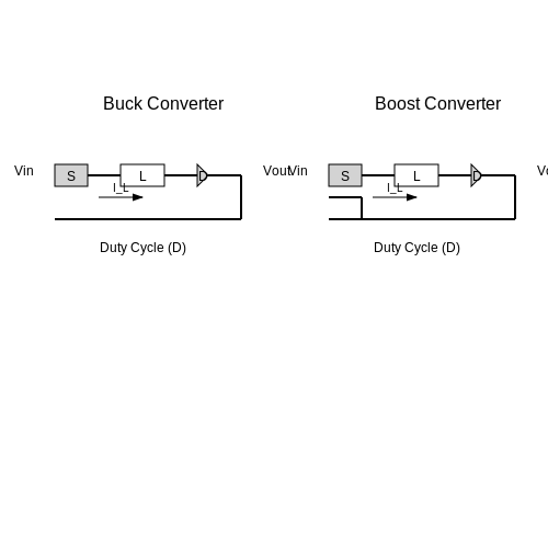
Zero-Voltage Transition Converters
1. Basic Principles of ZVT Operation
Basic Principles of ZVT Operation
Zero-Voltage Transition (ZVT) converters achieve high efficiency by ensuring that power switches turn on and off under zero-voltage conditions, eliminating switching losses. This is accomplished through resonant transitions, where an auxiliary circuit temporarily shapes the voltage or current waveform to create a zero-voltage crossing at the switching instant.
Resonant Transition Mechanism
The core principle relies on creating a resonant interval during which the voltage across the main switch is driven to zero before turn-on. This is typically achieved using an LC resonant tank formed by an auxiliary inductor (Lr) and capacitor (Cr). The auxiliary circuit, often comprising a small auxiliary switch and diode, is activated briefly before the main switch transitions.
When the resonant current equals the load current, the voltage across the main switch (vDS) reaches zero, enabling lossless turn-on. The duration of the resonant interval (tr) is derived from the LC tank's natural frequency:
Auxiliary Switch Timing
The auxiliary switch must be triggered just before the main switch to initiate resonance. Its conduction period (taux) is critical—too short, and the ZVT condition fails; too long, and excessive circulating currents increase conduction losses. The optimal timing balances these trade-offs:
Practical implementations often use a dead-time controller to synchronize the auxiliary and main switches, ensuring the main switch turns on precisely at the zero-voltage crossing.
Energy Recovery
ZVT topologies recover the energy stored in the resonant components (Lr, Cr) back to the input or output. For example, in a ZVT boost converter, the resonant inductor current discharges into the output capacitor during the switch-off phase, improving efficiency. The energy recovery efficiency (ηrec) is given by:
where ILr is the peak resonant current and RDS(on) is the switch on-resistance.
Practical Considerations
- Component Stress: The auxiliary switch must handle high peak currents during resonance, often requiring faster devices (e.g., GaN or SiC MOSFETs).
- Control Complexity: Precise timing demands advanced gate drivers or digital controllers (e.g., FPGA-based).
- EMI Reduction: Soft-switching minimizes dv/dt and di/dt, reducing high-frequency noise.
Modern ZVT designs integrate these principles into applications like server power supplies and EV chargers, where efficiency targets exceed 98%. For instance, a 1 kW ZVT phase-shifted full-bridge converter can achieve peak efficiencies of 98.5% at 500 kHz switching frequency.
1.2 Advantages of ZVT Over Hard Switching
Reduction in Switching Losses
Hard-switched converters suffer from significant switching losses due to the simultaneous occurrence of high voltage and current during transitions. The power loss during a switching event is given by:
where Vds is the drain-source voltage, Ids is the drain current, tr and tf are the rise and fall times, and fsw is the switching frequency. In Zero-Voltage Transition (ZVT) converters, the auxiliary circuit ensures that the main switch turns on or off when the voltage across it is near zero, effectively eliminating capacitive discharge losses and reducing overlap losses.
Improved Efficiency at High Frequencies
As switching frequencies increase to reduce passive component sizes, hard-switched converters experience exponential growth in switching losses. ZVT techniques enable operation at higher frequencies (1-10 MHz) while maintaining efficiency. Experimental results show efficiency improvements of 5-15% compared to hard-switched counterparts at comparable frequencies.
Reduced Electromagnetic Interference (EMI)
The abrupt voltage and current transitions in hard switching generate high dv/dt and di/dt, which are primary sources of conducted and radiated EMI. ZVT converters exhibit smoother transitions, reducing high-frequency harmonics. Measurements demonstrate a 10-20 dB reduction in EMI noise above 1 MHz.
Lower Stress on Semiconductor Devices
Hard switching subjects power devices to repetitive voltage and current stress peaks, accelerating device aging. The ZVT approach:
- Eliminates reverse recovery of body diodes in MOSFETs
- Reduces voltage overshoot during turn-off
- Minimizes thermal cycling effects
This results in improved reliability and longer operational lifetimes, particularly important in mission-critical applications.
Practical Implementation Considerations
While ZVT offers clear advantages, the auxiliary circuitry introduces additional complexity. The trade-offs include:
- Added component count (resonant inductors, auxiliary switches)
- Careful timing control requirements
- Slightly increased conduction losses in the auxiliary path
Modern control ICs with adaptive dead-time compensation and integrated gate drivers have made ZVT implementations more practical for commercial power supplies above 500W.
1.3 Key Applications of ZVT Converters
High-Efficiency Power Supplies
Zero-Voltage Transition (ZVT) converters are extensively used in high-efficiency power supplies where switching losses must be minimized. In applications such as server power supplies, telecom rectifiers, and industrial power systems, ZVT topologies enable operation at higher switching frequencies (100 kHz–1 MHz) while maintaining efficiency above 95%. The resonant transition mechanism eliminates capacitive discharge losses during switch turn-on, which is critical for wide-bandgap semiconductors like GaN and SiC devices operating at elevated frequencies.
Electric Vehicle Charging Systems
In onboard and offboard EV chargers, ZVT converters provide distinct advantages in bidirectional power flow configurations. The topology's soft-switching characteristics allow:
- Reduced thermal stress on MOSFETs/IGBTs in 400V–800V battery systems
- Higher power density through frequency scaling (enabling smaller magnetics)
- Compliance with CISPR 32 Class 3 EMI limits due to smoother switching transitions
Practical implementations often combine ZVT with phase-shifted full-bridge architectures for 3–22 kW charging stations.
Renewable Energy Conversion
Grid-tied solar inverters and wind power converters benefit from ZVT techniques in several ways:
Where conduction losses (Pcond) dominate at partial loads, while ZVT virtually eliminates switching losses (Psw). This results in >98% efficiency across wider operating ranges compared to hard-switched counterparts. The topology is particularly effective in:
- DC-DC boost stages for PV microinverters
- Medium-voltage conversion in wind turbine nacelles
- Battery interface circuits for hybrid renewable systems
Aerospace and Defense Power Systems
In aircraft electric power distribution (270V DC systems) and radar power modules, ZVT converters provide mission-critical reliability advantages:
- Elimination of voltage overshoot during switch transitions (reducing dV/dt stress)
- Intrinsic fault tolerance through resonant snubber networks
- Radiation-hardened operation via reduced semiconductor junction temperatures
Case studies show ZVT-based designs achieve MTBF >500,000 hours in satellite power conditioning units.
Medical Power Electronics
Medical imaging equipment (MRI gradient amplifiers, X-ray generators) utilizes ZVT converters to achieve:
- Ultra-low noise operation (<10 mVpp ripple at 10 kW)
- Precision current regulation (0.1% accuracy in therapeutic devices)
- Galvanic isolation with reduced transformer losses
The topology's predictable switching behavior also simplifies compliance with IEC 60601-1-2 electromagnetic compatibility standards.
Industrial Motor Drives
ZVT techniques are increasingly adopted in medium-voltage (2.3–6.6 kV) motor drives for:
Where the energy savings per switching cycle become substantial at bus voltages above 1 kV. Practical implementations show 30–40% reduction in heat sink requirements compared to conventional hard-switched inverters driving synchronous motors in compressor and pump applications.
2. ZVT Buck Converter
2.1 ZVT Buck Converter
The Zero-Voltage Transition (ZVT) buck converter is a resonant topology designed to minimize switching losses by ensuring that the main power switch turns on and off at zero voltage. This is achieved through an auxiliary resonant circuit that shapes the voltage and current waveforms, reducing hard-switching effects prevalent in conventional buck converters.
Operating Principle
The ZVT buck converter introduces an auxiliary switch and resonant inductor-capacitor (LC) network to create a soft-switching condition. The key operational phases are:
- Resonant Transition Phase: The auxiliary switch activates, initiating resonance between the inductor (Lr) and capacitor (Cr). This forces the voltage across the main switch to zero before turn-on.
- Power Delivery Phase: The main switch conducts, delivering energy to the load with minimal switching loss.
- Freewheeling Phase: The body diode of the synchronous rectifier (or a dedicated diode) conducts during the off-time, maintaining current continuity.
Mathematical Analysis
The resonant transition time (tr) is derived from the LC network’s natural frequency:
where Lr is the resonant inductance and Cr is the sum of the switch’s output capacitance and any additional snubber capacitance. The auxiliary circuit’s energy requirement must satisfy:
to fully discharge Cr before the main switch turns on. Here, Ipeak is the resonant inductor’s peak current, and Vin is the input voltage.
Design Considerations
Critical parameters for ZVT buck converter design include:
- Resonant Components: Lr and Cr must be chosen to ensure complete voltage transition within the dead time of the main switch.
- Auxiliary Switch Timing: The auxiliary switch must be activated just before the main switch to allow sufficient resonant transition.
- Loss Trade-offs: While ZVT reduces switching losses, the auxiliary circuit introduces conduction losses. Optimal design balances these effects.
Practical Applications
ZVT buck converters are favored in high-frequency (>1 MHz) and high-power applications, such as:
- Server power supplies, where efficiency at full load exceeds 95%.
- Electric vehicle charging systems, reducing thermal stress on semiconductor devices.
- Renewable energy inverters, enabling compact designs with higher power density.
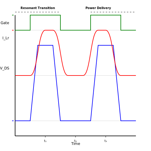
Waveforms and Timing Diagram
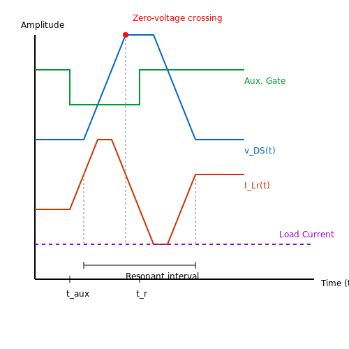
The following diagram illustrates key waveforms in a ZVT buck converter:
The main switch voltage (VDS) drops to zero during resonance, while the resonant inductor current (ILr) exhibits a sinusoidal profile. The auxiliary switch gate signal is timed to overlap with the resonant transition.
2.2 ZVT Boost Converter
The Zero-Voltage Transition (ZVT) Boost Converter is a high-efficiency DC-DC converter that minimizes switching losses by ensuring the main switch turns on and off at zero voltage. This is achieved through an auxiliary resonant circuit that shapes the voltage and current transitions, reducing stress on semiconductor devices.
Operating Principle
The ZVT Boost Converter operates in distinct stages:
- Resonant Transition Phase: An auxiliary switch activates a resonant inductor (Lr) and capacitor (Cr) to create a sinusoidal current path, discharging the output capacitance of the main switch.
- Main Conduction Phase: The main switch (S1) turns on at zero voltage, conducting the load current while the auxiliary circuit resets.
- Freewheeling Phase: The boost diode (D) carries the current during the switch-off period, maintaining output voltage regulation.
Mathematical Analysis
The resonant transition time (tr) is derived from the resonant tank parameters:
The voltage conversion ratio (M) of the ZVT Boost Converter, accounting for the resonant interval, is:
where D is the duty cycle and Ts is the switching period. The auxiliary circuit’s energy must satisfy:
Design Considerations
Key parameters for practical implementation include:
- Resonant Components: Lr and Cr must be selected to ensure complete discharge of the main switch’s capacitance within the dead time.
- Auxiliary Switch Timing: The auxiliary switch must be activated shortly before the main switch to allow sufficient resonant transition.
- Loss Trade-offs: While ZVT reduces switching losses, the auxiliary circuit introduces conduction losses that must be optimized.
Applications
ZVT Boost Converters are widely used in:
- Power Factor Correction (PFC): High-efficiency PFC stages in AC-DC converters.
- Renewable Energy Systems: Solar microinverters and wind turbine converters.
- Electric Vehicle Chargers: High-power DC-DC stages with minimal EMI.
The auxiliary resonant network (Lr, Cr) ensures soft switching, while the main inductor (L) and diode (D) follow conventional boost converter operation.
2.3 ZVT Buck-Boost Converter
The Zero-Voltage Transition (ZVT) Buck-Boost converter achieves soft-switching by ensuring that the main power switch turns on and off at zero voltage, minimizing switching losses. This topology combines the voltage step-up and step-down capabilities of a conventional buck-boost converter with resonant auxiliary circuitry to enable ZVT operation.
Operating Principle
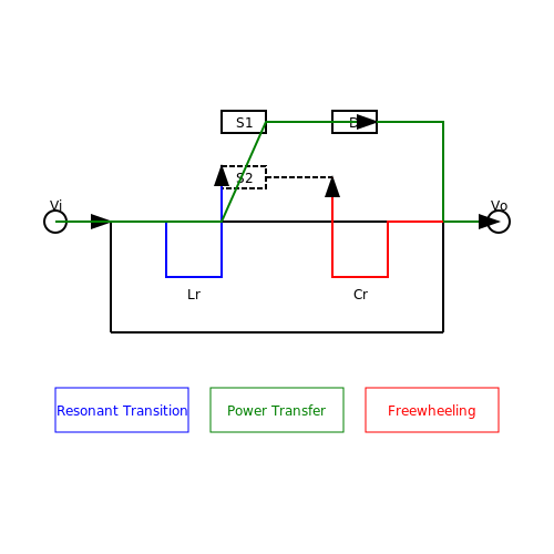
The ZVT Buck-Boost converter operates in distinct phases:
- Resonant Transition Phase: An auxiliary switch and resonant inductor-capacitor (LC) network create a resonant current path, discharging the main switch's parasitic capacitance to zero voltage before turn-on.
- Power Transfer Phase: The main switch conducts, transferring energy from the input to the output through the inductor, similar to a conventional buck-boost converter.
- Freewheeling Phase: The inductor current freewheels through the diode when the main switch turns off, with the auxiliary circuit ensuring zero-voltage turn-off.
Key Mathematical Derivation
The resonant transition time \( t_r \) is critical for proper ZVT operation. It is derived from the auxiliary LC network's resonant frequency:
where \( L_r \) is the resonant inductance and \( C_r \) is the sum of the switch output capacitance and any additional resonant capacitance.
The voltage conversion ratio \( M \) of the ZVT Buck-Boost converter is identical to the conventional buck-boost topology but with reduced switching losses:
where \( D \) is the duty cycle of the main switch.
Practical Implementation Considerations
Designing a ZVT Buck-Boost converter requires careful attention to:
- Resonant Component Selection: \( L_r \) and \( C_r \) must be chosen to ensure complete discharge of the main switch capacitance within the available dead time.
- Auxiliary Switch Timing: The auxiliary switch must be activated with precise timing relative to the main switch to ensure proper resonant transitions.
- Magnetic Design: The main inductor must handle both the power transfer current and the additional resonant current pulses without saturation.
Performance Advantages
The ZVT approach provides significant benefits in Buck-Boost converters:
- Reduced switching losses enable higher switching frequencies (typically 500kHz-2MHz range)
- Lower electromagnetic interference (EMI) due to softened switching transitions
- Improved efficiency, particularly at high input/output voltage ratios
- Better thermal performance due to reduced power dissipation in switches
Application Scenarios
ZVT Buck-Boost converters are particularly valuable in:
- Battery-powered systems with wide input voltage ranges
- High-frequency power supplies where switching losses dominate
- Applications requiring compact magnetics due to increased operating frequency
- Systems with stringent EMI requirements
2.4 Comparison of ZVT Topologies
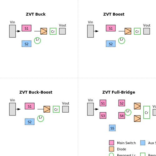
Zero-Voltage Transition (ZVT) converters employ various topologies to achieve soft-switching, each with distinct advantages and trade-offs in efficiency, complexity, and component stress. The most widely studied configurations include the ZVT buck, ZVT boost, ZVT buck-boost, and ZVT full-bridge converters.
ZVT Buck Converter
The ZVT buck converter integrates an auxiliary resonant circuit to ensure zero-voltage switching (ZVS) for the main switch. The resonant inductor (Lr) and capacitor (Cr) shape the current and voltage transitions, minimizing turn-on losses. The governing equations for the resonant transition are:
where tr is the resonant transition time. This topology excels in low-to-medium power applications (< 1 kW) due to its simplicity, but the auxiliary switch introduces conduction losses at higher loads.
ZVT Boost Converter
In ZVT boost converters, the auxiliary circuit ensures ZVS for the main switch while mitigating reverse recovery losses in the output diode. The resonant components are designed such that:
where VCr,peak and ILr,peak are the peak resonant capacitor voltage and inductor current, respectively. This topology is favored in power factor correction (PFC) circuits but suffers from higher voltage stress on the main switch compared to the buck variant.
ZVT Buck-Boost Converter
The ZVT buck-boost converter combines features of both buck and boost topologies, enabling bidirectional power flow. The resonant transition is governed by:
where fr is the resonant frequency. This configuration is versatile but requires careful tuning of Lr and Cr to avoid excessive circulating energy.
ZVT Full-Bridge Converter
Full-bridge ZVT topologies are employed in high-power applications (> 5 kW), such as industrial motor drives and renewable energy systems. The phase-shifted control ensures ZVS for all primary-side switches, with the resonant transition described by:
where Z0 is the characteristic impedance. While highly efficient, this topology demands precise dead-time control and suffers from higher component count.
Comparative Analysis
The table below summarizes key metrics across topologies:
| Topology | Efficiency Range | Voltage Stress | Typical Applications |
|---|---|---|---|
| ZVT Buck | 92–96% | Low | Point-of-load converters |
| ZVT Boost | 90–94% | High | PFC, solar inverters |
| ZVT Buck-Boost | 88–92% | Moderate | Battery chargers |
| ZVT Full-Bridge | 94–98% | Very High | High-power DC-DC |
Designers must weigh trade-offs between efficiency, component stress, and control complexity when selecting a ZVT topology. For instance, the full-bridge converter achieves the highest efficiency but at the cost of increased circuit complexity and sensitivity to parasitic elements.
3. Resonant Components Selection
3.1 Resonant Components Selection
The selection of resonant components—primarily the inductor (Lr) and capacitor (Cr)—dictates the efficiency and soft-switching performance of a Zero-Voltage Transition (ZVT) converter. The resonant tank must be designed to ensure zero-voltage switching (ZVS) across the intended load range while minimizing circulating energy.
Resonant Frequency and Characteristic Impedance
The resonant frequency (fr) and characteristic impedance (Zr) are derived from the inductor-capacitor interaction:
For ZVT operation, fr is typically set 5–10 times higher than the converter's switching frequency (fsw) to limit resonant interval duration. A higher Zr reduces peak resonant current but may increase voltage stress.
Trade-offs in Component Selection
- Inductor (Lr): A smaller value reduces energy storage but increases peak current, raising conduction losses. Core material must handle high di/dt without saturation.
- Capacitor (Cr): A larger value lowers voltage stress but extends resonant transition time. Low-ESR film or ceramic capacitors are preferred for high-frequency operation.
Design Procedure
To achieve ZVS, the resonant tank must satisfy:
where Ipk is the peak inductor current and Vin is the input voltage. Rearranging for Lr and Cr:
Practical designs often iterate between these parameters, considering:
- Parasitic capacitances (e.g., MOSFET output capacitance) that add to Cr.
- Load-dependent damping effects, which alter the resonant waveform.
Practical Example
For a 1 kW ZVT boost converter with Vin = 200 V, fsw = 100 kHz, and a target resonant frequency of 500 kHz:
Selecting Cr = 2.2 nF (including parasitics) yields Lr ≈ 46 µH. Verify ZVS condition at minimum load (e.g., 10% of rated power) to ensure robustness.
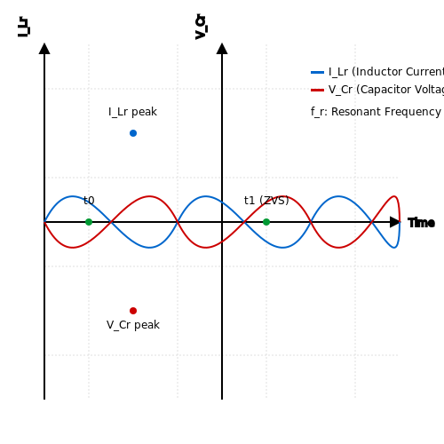
The above waveform illustrates the ideal resonant transition, where the capacitor voltage (VCr) reaches zero before the switch turns on. Deviations indicate insufficient energy or improper damping.
3.2 Switching Frequency Optimization
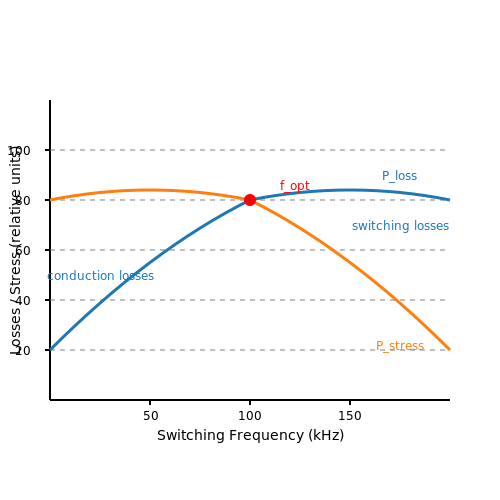
Switching frequency optimization in zero-voltage transition (ZVT) converters involves balancing trade-offs between efficiency, component stress, and electromagnetic interference (EMI). Higher frequencies reduce passive component size but increase switching losses and stress on semiconductor devices. The optimal frequency is derived from a multi-objective analysis of converter dynamics.
Loss Mechanisms and Frequency Dependence
Total converter losses Ploss consist of conduction losses Pcond and switching losses Psw:
Conduction losses scale with RMS current and on-state resistance:
Switching losses exhibit linear frequency dependence due to hard switching:
where tr and tf are rise/fall times, and fsw is switching frequency.
ZVT-Specific Loss Considerations
In ZVT topologies, the auxiliary circuit enables soft switching but introduces additional components with their own loss contributions:
- Auxiliary switch losses - IGBT/MOSFET conduction and turn-off losses
- Resonant inductor losses - Core losses (proportional to f1.3-2.0) and copper losses
- Snubber capacitor ESR losses - Dielectric absorption at high frequencies
Optimal Frequency Derivation
The system-level optimization problem minimizes total losses subject to constraints:
where coefficients k1, k2, and k3 capture:
- Semiconductor switching losses (linear term)
- Magnetic component size (inverse term)
- High-frequency parasitic effects (exponential term)
Differentiating and solving yields the optimal frequency:
Practical Implementation Considerations
Real-world implementations must account for:
- Gate driver limitations - Propagation delays become significant above 500kHz
- PCB layout parasitics - Stray inductance causes voltage overshoot at high di/dt
- Thermal management - Power density vs. heat dissipation tradeoffs
Modern wide-bandgap devices (GaN, SiC) shift the optimal frequency upward due to faster switching capabilities and lower Qrr.
3.3 Loss Analysis and Efficiency Improvement
Switching Loss Mechanisms in ZVT Converters
Zero-Voltage Transition (ZVT) converters significantly reduce switching losses compared to hard-switched counterparts, but residual losses persist due to non-ideal conditions. The primary loss components include:
- Conduction losses in the main switch, auxiliary switch, and resonant inductor
- Capacitive discharge losses during the transition phase
- Reverse recovery losses in body diodes
- Gate drive losses from high-frequency switching
The total power dissipation Ptotal can be expressed as:
Quantifying Conduction Losses
Conduction losses dominate at high load currents. For a MOSFET with on-resistance RDS(on) and current Irms:
where D is the duty cycle. The RMS current through the auxiliary switch differs from the main switch due to resonant operation:
Switching Loss Reduction Analysis
ZVT converters eliminate voltage-current overlap during turn-on, but partial overlap remains during turn-off. The residual switching energy Esw is:
where Coss is the output capacitance, tf is the fall time, and Vds is the drain-source voltage.
Resonant Component Optimization
The resonant inductor and capacitor values critically impact efficiency. The optimal resonant period Tres should satisfy:
Excessive resonance duration increases conduction losses, while insufficient duration fails to achieve complete ZVT. The quality factor Q should be maintained in the range 1-2 for optimal performance:
Practical Efficiency Enhancement Techniques
- Dead-time optimization between main and auxiliary switch control signals
- Adaptive gate driving that adjusts strength based on load current
- Synchronous rectification for the auxiliary path
- Integrated magnetics to reduce core losses in the resonant inductor
The impact of these techniques can be modeled through the converter's equivalent resistance Req:
Thermal Considerations
Loss distribution affects thermal management requirements. The junction temperature rise ΔT can be estimated using:
where Rth,j-c is the thermal resistance from junction to case. Proper heatsinking must account for both conduction and switching loss components.
4. Component Stress and Thermal Management
4.1 Component Stress and Thermal Management
In zero-voltage transition (ZVT) converters, component stress arises primarily from high-frequency switching, voltage/current spikes, and thermal dissipation. The primary contributors include the main switch (MOSFET/IGBT), auxiliary resonant components, and output diodes. Understanding these stresses is critical for reliability and efficiency.
Switch Stress Analysis
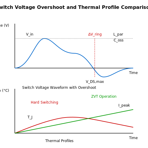
The main switch experiences reduced turn-on losses due to ZVT operation, but turn-off losses and voltage overshoot remain concerns. The peak voltage stress (VDS,max) can be derived from the resonant transition dynamics:
where ΔVring is the overshoot caused by parasitic inductance (Lpar) and switch capacitance (Coss):
For example, a 100V input converter with 10nH parasitic inductance and 500pF output capacitance at 20A peak current exhibits a 63V overshoot, pushing the switch to 163V—a 63% increase.
Diode Reverse Recovery Stress
The output diode's reverse recovery charge (Qrr) generates current spikes during commutation. In ZVT topologies, this is mitigated by the auxiliary circuit's soft switching, but residual effects persist due to:
- Non-ideal resonant timing
- Parasitic capacitance discharge
- Temperature-dependent recovery characteristics
The reverse recovery power loss is approximated by:
Thermal Management Strategies
Effective thermal design requires analyzing power dissipation across three domains:
- Conduction losses: Dominated by RDS(on) and forward voltage drops.
- Switching losses: Reduced but not eliminated by ZVT operation.
- Reverse recovery losses: Diode-dependent and frequency-sensitive.
The total junction temperature rise is calculated using thermal impedance (θJA):
Practical implementations use:
- Kelvin-source PCB layouts to reduce parasitic inductance
- Active gate drive shaping to control dv/dt
- Phase-change materials for high-power density modules
Case Study: 1kW ZVT Boost Converter
A 400V output design with GaN switches shows:
| Parameter | Hard Switching | ZVT Implementation |
|---|---|---|
| Switch Losses | 22W | 8W |
| Diode Losses | 15W | 6W |
| Peak Junction Temp | 128°C | 94°C |
The thermal improvement enables 30% higher power density while maintaining reliability margins.
4.2 Control Strategy for ZVT Operation
The control strategy for Zero-Voltage Transition (ZVT) converters is critical to achieving soft-switching conditions, minimizing switching losses, and improving overall efficiency. The primary objective is to ensure that the main power switch turns on and off under zero-voltage conditions, eliminating voltage-current overlap losses. This requires precise timing of auxiliary circuit activation and synchronization with the main switching cycle.
Key Control Parameters
The control strategy hinges on three fundamental parameters:
- Resonant Inductor Current (Lr) — Determines the energy required to discharge the output capacitance of the main switch.
- Resonant Capacitor Voltage (Cr) — Governs the resonant transition period during which the switch voltage falls to zero.
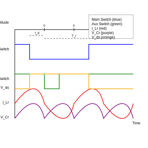
- Dead Time (td) — The interval between turning off the auxiliary switch and turning on the main switch, ensuring zero-voltage conditions.
Mathematical Derivation of ZVT Timing
The resonant transition period Tr is derived from the natural resonant frequency of the Lr-Cr tank circuit:
The time required to fully discharge the output capacitance Coss of the main switch is:
To ensure complete discharge before the main switch turns on, the dead time td must satisfy:
Implementation Techniques
Two prevalent control methods are employed in ZVT converters:
- Fixed-Frequency Pulse Width Modulation (PWM) — The auxiliary circuit is triggered at a fixed phase relative to the main switch gate signal, ensuring repeatable ZVT conditions.
- Variable Timing with Feedback — A closed-loop controller dynamically adjusts the auxiliary switch timing based on load current and input voltage variations.
Fixed-Frequency PWM Control
In this approach, the auxiliary switch is activated a fixed delay td before the main switch turn-on instant. The gate signals for both switches are synchronized to the PWM carrier waveform. The resonant inductor current must satisfy:
where Zr is the characteristic impedance of the resonant tank:
Variable Timing with Feedback
For wide input voltage or load ranges, adaptive control is necessary. A feedback loop monitors the drain-source voltage of the main switch and adjusts the auxiliary switch timing to ensure zero-voltage switching under all conditions. The control law can be expressed as:
where Vth is a threshold voltage (typically 5-10% of Vin), and Kp, Ki are proportional and integral gains.
Practical Considerations
In real implementations, several non-idealities must be accounted for:
- Parasitic capacitances and inductances in the layout can alter resonant behavior.
- Gate drive propagation delays must be compensated in the timing calculations.
- The auxiliary switch conduction losses increase at light loads, potentially reducing efficiency.
Modern digital signal processors (DSPs) and field-programmable gate arrays (FPGAs) are increasingly used to implement sophisticated adaptive ZVT control algorithms, enabling efficiency optimization across wide operating ranges.
4.3 EMI and Noise Reduction Techniques
Sources of EMI in Zero-Voltage Transition Converters
Electromagnetic interference (EMI) in zero-voltage transition (ZVT) converters primarily arises from high-frequency switching transitions, parasitic inductances, and capacitive couplings. The rapid dv/dt and di/dt during soft-switching events generate common-mode (CM) and differential-mode (DM) noise. Key contributors include:
- Parasitic ringing due to resonant tank interactions with stray inductances and capacitances.
- Ground loops introduced by improper layout or grounding schemes.
- Radiated emissions from high-current loop areas and unshielded components.
Active Noise Cancellation Techniques
Active techniques dynamically counteract EMI by injecting compensating signals. For ZVT converters, this often involves:
where k is the feedback gain and Lstray is the parasitic inductance. Practical implementations use:
- Feedforward correction with high-bandwidth current sensors to preemptively adjust gate drive timing.
- Adaptive filtering in control loops to suppress specific harmonic content.
Passive Filter Design
Passive filters remain critical for broadband attenuation. A second-order LC filter's cutoff frequency for DM noise is:
For CM noise, a well-designed choke with balanced winding capacitance is essential. The impedance ZCM of a common-mode choke is given by:
where Rw is the winding resistance and Cpar is the interwinding capacitance.
Layout Optimization
Key principles for PCB layout include:
- Minimizing loop areas by placing high-di/dt paths (e.g., switch-node traces) adjacent to return paths.
- Segregating analog and power grounds with star-point connections to avoid ground bounce.
- Using multilayer designs with dedicated power and ground planes to reduce parasitic coupling.
Shielding and Component Selection
Ferrite beads and shielded inductors suppress high-frequency resonances. The effectiveness of a ferrite bead is quantified by its impedance curve:
where R(ω) dominates at frequencies beyond the bead's self-resonance. For capacitors, low-ESR ceramic types (e.g., X7R) are preferred for decoupling.
Case Study: ZVT Boost Converter
In a 1 kW ZVT boost converter operating at 500 kHz, implementing a combination of:
- Active gate drive shaping (reducing dv/dt by 40%).
- Common-mode chokes with >50 dB attenuation above 10 MHz.
- Four-layer PCB with 2 oz copper.
resulted in a 12 dB reduction in conducted EMI across the 150 kHz–30 MHz band.
5. Key Research Papers on ZVT Converters
5.1 Key Research Papers on ZVT Converters
- Novel zero-voltage-transition PWM converters - IEEE Xplore — A class of zero voltage transition (ZVT) power converters is proposed in which both the transistor and the rectifier operate with zero voltage switching and are subjected to minimum voltage and current stresses. The boost ZVT-PWM converter is used as an example to illustrate the operation of these converters. A 300 kHz, 600 W ZVT-PWM boost, DC-DC converter, and a 100 kHz, 600 W power factor ...
- A Family of ZVT DC-DC Converters With Low-Voltage Ringing — In this paper, a new low-voltage ringing zero voltage transition (ZVT) cell is proposed for a family of non-isolated dc-dc converters. In the proposed converter, all semiconductor devices operate under soft-switching condition at both turning on and off. The proposed ZVT cell resolves the issues appeared in the previous works: no online calculation required to achieve ZVS turn-on of the main ...
- Zero voltage transition-zero current transition pulse‐width modulated ... — In this study, a zero voltage transition (ZVT)-zero current transition (ZCT) pulse-width modulated (PWM) multiphase synchronous buck converter (SBC), with an active auxiliary circuit is proposed, that reduces the stresses and enhances the efficiency abating the switching and conduction losses of the converter.
- PDF Implementation of Soft Switched Low Stress ZVT PWM Converter for ... — converter. Thus, the ZVT-PWM converter can achieve soft switching without increasing the voltage stresses of active power switches. Soft-switching power converters can be classified as ZVS/ zero-current-switching (ZCS) PWM power converters or ZVT/ZCT soft-switching power converters. The auxiliary switch forms a resonant loop,
- A ZVT-ZCT PWM synchronous buck converter with a simple passive ... — In this paper, a Zero-Voltage-Transition (ZVT)-Zero-Current Transition (ZCT) Pulse-width Modulated (PWM) synchronous buck converter (SBC), with a simple passive auxiliary circuit is proposed, which reduces the stresses and improves the efficiency by pacifying the conduction losses compared to a traditional PWM converter, typically suitable for photovoltaic applications.
- A Modular AC-DC Power Converter with Zero Voltage Transition for ... - MDPI — A study of the fundamental of operation of a three-phase AC-DC power converter that uses Zero-Voltage Transition (ZVT) together with Space Vector Pulse Width Modulation (SVPWM) is presented. The converter is basically an active rectifier divided into two converters: a matrix converter and an H bridge, which transfer energy through a high-frequency transformer, resulting in a modular AC-DC ...
- (PDF) Development of Improved Performance Switchmode Converters for ... — International Journal for Research in Applied Science and Engineering Technology IJRASET, 2020. In this paper, a Zero Voltage Transition (ZVT)-Zero current Transition (ZCT) Pulse-width Modulated (PWM) multiphase synchronous buck converter (SBC), with an active auxiliary circuit is proposed, that reduces the stresses and enhances the efficiency abating the switching and conduction losses of the ...
- Three-level boost converter with zero voltage transition — In this paper, a ZVT three-level boost converter is proposed. With the proposed ZVT circuit, the switches of the three-level boost converter can be turned on at zero voltage. Moreover, since the output voltage is shared by two output capacitors, a voltage balance control is employed to balance the output capacitor voltages. 2 Three-level boost ...
- A Zero Voltage Transition enabled Inverting Non-Isolated Synchronous ... — The proposed ZVT-enabled INSBB converter was comprehensively evaluated across key performance metrics to ensure practical applicability. As shown in Fig. 17 , the converter achieves a peak efficiency of 97.5% at 600 W and 94.2% at 300 W, primarily due to the ZVT technique, significantly reducing switching and reverse recovery losses.
- A ZVT-ZCT PWM synchronous buck converter with a simple passive ... — In this paper, a Zero-Voltage-Transition (ZVT) Pulsewidth Modulated (PWM) synchronous buck converter (SBC), with a simple passive auxiliary circuit is proposed, which reduces the stresses and ...
5.2 Recommended Books on Power Electronics
- Power Electronics Handbook - 5th Edition - Elsevier Shop — Purchase Power Electronics Handbook - 5th Edition. Print Book & E-Book. ISBN 9780323992169, 9780323993432 ... Zero-Voltage-Transition Converters. 11.8: Non-Dissipative Active Clamp Network. 11.9: Load-Resonant Converters ... Thermal Modeling and Analysis for Power Electronic Components and Systems. Abstract. 44.1: Introduction. 44.2: Background ...
- Soft-Switching Technology for Three-phase Power Electronics Converters — 2.5.2 Coupled-inductor Zero Voltage-transition (ZVT) Inverter 59 2.5.3 Zero-current Transition (ZCT) Inverter 62 2.6 Soft-switching Inverter with TCM Control 62 2.7 Summary 66 References 67 3 Soft-switching PWM Control for Active Clamped Three-phase Converters 71 3.1 Introduction 71 3.2 PWM of Three-phase Converters 72 3.3 Edge-aligned PWM 76 3 ...
- Fundamentals Of Power Electronics: Book For Instructors [PDF ... — in a nonideal boost converter, 48-49, 56 in a nonideal buck converter, 52-53 in small-signal ac CCM models, 208-210 Decibel, 262 Delta-wye transformer connection, 582-583 Dependent power source (see Power source element) Derating factor, 180 Design-oriented analysis, techniques of analytical expressions for asymptotes, 275-276 approximate ...
- Power Electronics Converters—An Overview - ScienceDirect — Power electronics converters use electronic components based on semiconductor switches operated at different frequency levels from 50 to 60 Hz mains frequencies to 100 MHz radio frequency. In order to optimally support different features of diverse applications, power electronics converters should benefit from different characteristics such as ...
- An overview of power electronic converter technology for renewable ... — Semiconductors, being basic power electronic components and acting as switches in power electronic circuits, may be classified as non-controllable, AC voltage-commutated and self-commutated (switchable) semiconductors as shown in Fig. 4.1.Diodes are non-controllable devices in which on and off states are completely determined by external circuit conditions.
- 16. Resonant and Soft-switching Converters - POWER ELECTRONICS HANDBOOK ... — 16.7 Zero-voltage-transition (ZVT) Converters Get POWER ELECTRONICS HANDBOOK, 3rd Edition now with the O'Reilly learning platform. O'Reilly members experience books, live events, courses curated by job role, and more from O'Reilly and nearly 200 top publishers.
- Overview of Power Electronics Converters and Controls - ResearchGate — Overwiew of Power Electronics Converters and Controls 73 In a zero-voltage resonant switch (Fig ure 3.20b), a capacitor C r is connected in parallel with the switch S in order to create ZVS ...
- Resonant and Soft-Switching Converters - ScienceDirect — In the 1980s, lots of research efforts were diverted toward the use of resonant converters. The concept was to incorporate resonant tanks in the converters to create oscillatory (usually sinusoidal) voltage and/or current waveforms so that zero-voltage switching (ZVS) or zero-current switching (ZCS) conditions can be created for the power switches.
- Power Electronics Handbook, 4th Edition[Book] - O'Reilly Media — Book description. Power Electronics Handbook, Fourth Edition, brings together over 100 years of combined experience in the specialist areas of power engineering to offer a fully revised and updated expert guide to total power solutions. Designed to provide the best technical and most commercially viable solutions available, this handbook undertakes any or all aspects of a project requiring ...
- Power Electronics Handbook, 5th Edition - Anna's Archive — 📚 The largest truly open library in human history. ⭐️ We mirror Sci-Hub and LibGen. We scrape and open-source Z-Lib, DuXiu, and more. 📈 43,206,948 books, 98,551,629 papers — preserved forever.
5.3 Online Resources and Tutorials
- Soft-Switching Technology for Three-phase Power Electronics Converters — 2.5.2 Coupled-inductor Zero Voltage-transition (ZVT) Inverter 59 2.5.3 Zero-current Transition (ZCT) Inverter 62 2.6 Soft-switching Inverter with TCM Control 62 2.7 Summary 66 References 67 3 Soft-switching PWM Control for Active Clamped Three-phase Converters 71 3.1 Introduction 71 3.2 PWM of Three-phase Converters 72 3.3 Edge-aligned PWM 76 3 ...
- PDF Soft-Switching Technology for Three-phase — 2.5.2 Coupled-inductor Zero Voltage-transition (ZVT) Inverter 59 2.5.3 Zero-current Transition (ZCT) Inverter 62 2.6 Soft-switching Inverter with TCM Control 62 2.7 Summary 66 References 67 3 Soft-switching PWM Control for Active Clamped Three-phase Converters 71 3.1 Introduction 71 3.2 PWM of Three-phase Converters 72 3.3 Edge-aligned PWM 76 3 ...
- Three-level boost converter with zero voltage transition — half-wave mode [21-23], active clamp [24-36], zero voltage transi-tion (ZVT) [37-48], zero current transition [49-51], and ZCTZVT [52, 53]. In this paper, a ZVT three-level boost converter is proposed. With the proposed ZVT circuit, the switches of the three-level boost converter can be turned on at zero voltage. Moreover, since the ...
- Three-level boost converter with zero voltage transition — 3 Basic operating principles. The voltage and current symbols shown in Fig. 1 b, and the assumptions are given as follows: (i) V i is the DC input voltage; (ii) V o is the DC output voltage; (iii) is the current flowing through the resonant inductor L r; (iv) v Cs 1 and v Cs 2 are the voltages across the parasitic capacitances C s 1 and C s 2 or the main switches S 1 and S 2, respectively; (v ...
- PDF A Zero-Voltage Switching Technique for High Frequency Buck Converter ICs — ) in the main switch node, bringing the voltage up to the input voltage. Once the main switch node voltage is equal to the input voltage, we can turn on with zero voltage across it, hence achieving zero voltage switching. We 15
- A ZVT-ZCT PWM synchronous buck converter with a simple passive ... — A new family of zero-voltage transition PWM converters with dual active auxiliary circuits. IEEE Trans Power Electron, 21 (2) (2006), pp. 370-379 [March] View ... India, in 1987. He received the M.Tech. in Power Electronics and Drives from Indian Institute of Technology, Kharagpur, India, in 1993 and Ph.D. in 2001 from Utkal University. Join as ...
- PDF ZVS Boost Converter - University of Central Florida — EEL6246 Power Electronics II Chapter 6 - Lecture 6 Dr. Sam Abdel-Rahman Example 6.5 Design a ZVS-QRC boost converter for the following design parameters: V in =30V, P 0=30W at V0=38V, fns =0.4, and T s=4 µs. Assume the output voltage ripple is limited to 2% at D = 0.4. Solution: The voltage gain is and with fns = 0.4, we obtain Q = 0.2 ...
- A Modular AC-DC Power Converter with Zero Voltage Transition for ... - MDPI — A study of the fundamental of operation of a three-phase AC-DC power converter that uses Zero-Voltage Transition (ZVT) together with Space Vector Pulse Width Modulation (SVPWM) is presented. The converter is basically an active rectifier divided into two converters: a matrix converter and an H bridge, which transfer energy through a high-frequency transformer, resulting in a modular AC-DC ...
- Coupled inductor based zero-voltage-switching buck/boost converter ... — This paper proposes a zero-voltage-switching (ZVS) Buck/Boost converter (BBC). In addition, an auxiliary circuit based on a coupled inductor is introduced to realize ZVS for the main MOSFETs. The magnetic coupling inductor plays the role of filtering and provides ZVS conditions for the main MOSFETs. Since all of the switches can achieve soft switching conditions, and the conduction loss of the ...
- A Variable-Frequency ZVS Modulation for Four-Switch Buck+Boost ... — This paper introduces variable-frequency zero voltage switching (ZVS) modulation strategy for the four-switch buck+boost converter with one operating pattern for the inductor current, i.e., three-segment inductor current modulation control. The proposed modulation scheme guarantees a smooth transition from step-up to step-down or from step-down to step-up operating modes without abrupt duty ...