Micro-LED Display Technology
1. Basic Principles of Micro-LEDs
Basic Principles of Micro-LEDs
Fundamental Structure and Operation
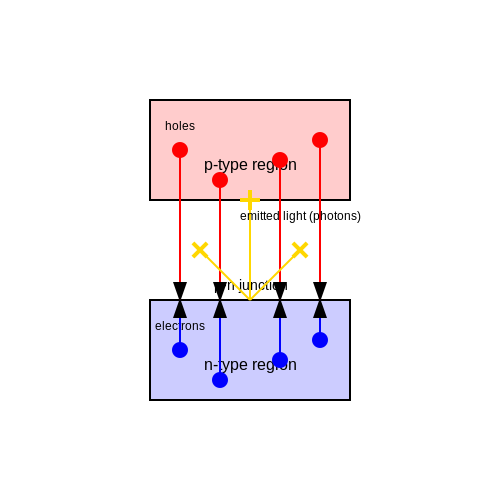
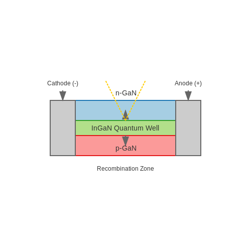
Micro-LEDs are inorganic light-emitting diodes with pixel sizes typically below 50 micrometers. Unlike conventional LEDs, they operate as individual emissive elements without requiring additional backlighting or color filters. The basic structure consists of an n-type semiconductor, active quantum well region, and p-type semiconductor, fabricated using epitaxial growth techniques such as metal-organic chemical vapor deposition (MOCVD).
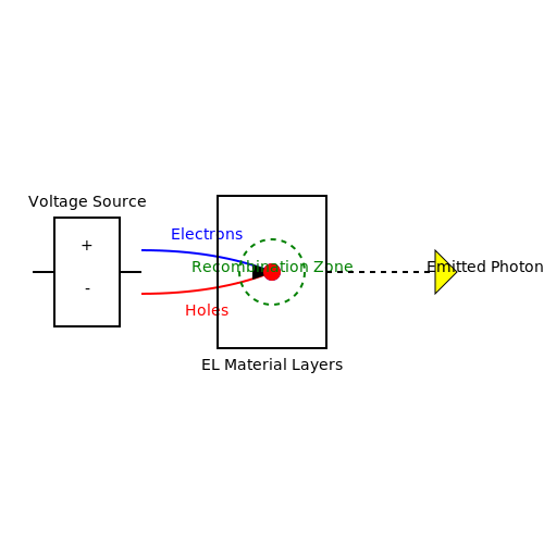
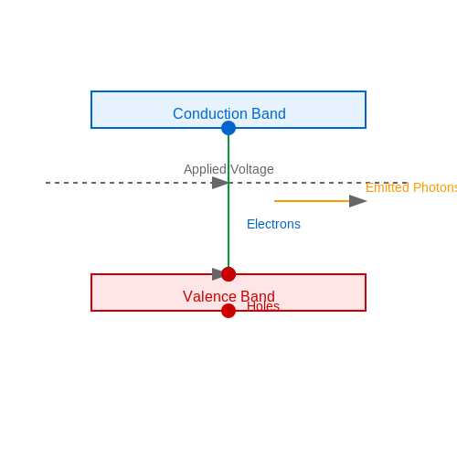
When forward-biased, electrons and holes recombine in the quantum wells, emitting photons with energy corresponding to the bandgap of the semiconductor material. The wavelength λ of emitted light is determined by:
where h is Planck's constant, c is the speed of light, and Eg is the material bandgap energy.
Key Performance Metrics
The electro-optical characteristics of Micro-LEDs are governed by three primary parameters:
- External Quantum Efficiency (EQE): The ratio of emitted photons to injected electrons, typically ranging from 5-50% depending on size and fabrication quality.
- Current Density (J): Operating currents can exceed 1000 A/cm² due to the small active area.
- Modulation Bandwidth: Micro-LEDs can achieve >100 MHz bandwidth, enabling visible light communication applications.
The light output power Pout relates to the input current I through:
Size-Dependent Effects
As pixel dimensions shrink below 20 μm, several quantum mechanical phenomena become significant:
- Surface recombination: Dominates over bulk recombination due to increased surface-to-volume ratio.
- Current crowding: Non-uniform current distribution leads to localized heating.
- Quantum confinement: Alters the density of states in ultra-small structures.
The modified Shockley-Read-Hall recombination rate RSRH accounts for these effects:
where S is the surface recombination velocity and τ are carrier lifetimes.
Fabrication Challenges
Mass transfer of individual Micro-LED dies remains the primary manufacturing bottleneck. Current approaches include:
- Pick-and-place assembly (for >30 μm pixels)
- Elastomer stamp transfer
- Fluidic self-assembly
- Monolithic integration (for micro-displays)
The transfer yield Y required for commercial viability follows:
For a 4K display (8.3 million pixels), this demands >99.99999% yield per transfer operation.
Color Conversion Techniques
Full-color Micro-LED displays employ several approaches:
- Direct emission: Using separate red, green, and blue (RGB) Micro-LED pixels
- Quantum dot conversion: Blue Micro-LEDs with photoluminescent quantum dots
- Wavelength down-conversion: UV Micro-LEDs with phosphor coatings
The color gamut coverage C for quantum dot conversion is given by:
where A represents the area in CIE 1931 color space, with state-of-the-art systems achieving >110% NTSC.
1.2 Comparison with OLED and LCD Technologies
Efficiency and Power Consumption
Micro-LEDs exhibit superior luminous efficiency compared to OLEDs and LCDs due to their inorganic semiconductor nature. The external quantum efficiency (EQE) of Micro-LEDs can exceed 50%, whereas OLEDs typically achieve 20–30% due to non-radiative recombination losses. LCDs, relying on backlight absorption, suffer further inefficiencies, with only 5–10% of light transmitted through color filters.
Here, ηinj is the carrier injection efficiency, ηrad the radiative recombination efficiency, and ηext the light extraction efficiency. Micro-LEDs minimize non-radiative losses (ηrad ≈ 1) and optimize ηext via advanced packaging.
Contrast Ratio and Black Levels
Micro-LEDs and OLEDs both achieve near-infinite contrast ratios by enabling per-pixel illumination, unlike LCDs that rely on liquid crystal shutters leaking light. However, Micro-LEDs avoid OLED’s organic material degradation, which causes brightness decay and elevated black levels over time.
Response Time and Motion Blur
Micro-LED response times (<1 μs) surpass OLEDs (~10 μs) and LCDs (~1–10 ms). This eliminates motion blur in high-frame-rate applications (e.g., VR, gaming). The transition speed stems from direct bandgap recombination in GaN-based Micro-LEDs, bypassing liquid crystal realignment or exciton lifetime delays.
Color Gamut and Stability
Micro-LEDs cover >120% NTSC color space using nitride semiconductors, while OLEDs achieve ~100% NTSC but suffer from differential aging of RGB emitters. LCDs, limited by backlight spectra and filter purity, reach 70–90% NTSC. Micro-LEDs also maintain color stability at high brightness (>10,000 nits), unlike OLEDs prone to luminance roll-off.
Lifetime and Reliability
Micro-LEDs demonstrate >100,000 hours operational lifetime, outperforming OLEDs (~30,000 hours) due to inorganic material resilience against oxidation and thermal degradation. LCDs, while durable, face backlight degradation (e.g., CCFL/LED lumen depreciation).
Manufacturing Complexity
Micro-LED production involves epitaxial growth, mass transfer, and bonding—challenging for high-density displays. OLEDs simplify fabrication via vapor deposition but require encapsulation. LCDs remain the most mature, leveraging established thin-film transistor (TFT) processes.
Applications and Trade-offs
- Micro-LEDs: High-end AR/VR, large-area displays (modular tiling), and HDR applications where efficiency and longevity are critical.
- OLEDs: Consumer electronics (smartphones, TVs) prioritizing thinness and flexibility.
- LCDs: Cost-sensitive, high-volume markets (monitors, laptops) where color accuracy suffices.
1.3 Key Advantages of Micro-LED Displays
Superior Brightness and Contrast Ratio
Micro-LED displays achieve significantly higher brightness levels compared to OLED and LCD technologies, often exceeding 10,000 nits under optimal conditions. This is due to the inherent luminance efficiency of inorganic LED materials, which do not suffer from the thermal degradation or burn-in issues common in OLEDs. The contrast ratio is also superior, as Micro-LEDs can achieve true blacks by completely turning off individual pixels, similar to OLED, but without the risk of pixel degradation over time.
Energy Efficiency and Power Consumption
The power efficiency of Micro-LEDs stems from their ability to emit light directly without requiring a backlight (as in LCDs) or organic materials (as in OLEDs). The luminous efficacy can be derived from the radiative recombination efficiency:
where ηint is the internal quantum efficiency and ηextraction is the light extraction efficiency. For typical Micro-LEDs, ηext can exceed 50%, significantly higher than OLEDs (20-30%) or LCDs with backlights (5-15%).
Longevity and Reliability
Micro-LEDs utilize inorganic gallium nitride (GaN) or similar semiconductor materials, which are far more stable than the organic compounds in OLEDs. Accelerated lifetime testing shows that Micro-LEDs can operate for over 100,000 hours with minimal luminance decay, whereas OLEDs typically degrade noticeably after 10,000-20,000 hours. This makes Micro-LEDs ideal for applications requiring long-term reliability, such as medical displays or aerospace instrumentation.
High Resolution and Pixel Density
With pixel pitches as small as 5-10 microns, Micro-LEDs enable pixel densities exceeding 2000 PPI (pixels per inch). This is achieved through advanced epitaxial growth and mass transfer techniques. The modulation transfer function (MTF) for a Micro-LED array can be modeled as:
where f is the spatial frequency and p is the pixel pitch. The smaller p in Micro-LEDs allows for higher MTF values at given frequencies compared to other display technologies.
Wide Color Gamut and Fast Response Time
Micro-LEDs can cover over 140% of the NTSC color space due to the narrow spectral emission lines of their quantum well structures. The response time is in the nanosecond range (typically < 100 ns), orders of magnitude faster than LCDs (ms range) and slightly better than OLEDs (µs range). This combination makes them ideal for high-frame-rate applications like virtual reality or scientific visualization.
Modularity and Scalability
Micro-LED displays can be tiled seamlessly to create large-area displays with no visible bezels. The modular nature arises from the individual addressability of each Micro-LED pixel and the use of active matrix backplanes. This scalability is particularly valuable for applications ranging from small wearable devices to massive video walls in control rooms or broadcast studios.
Environmental Robustness
Unlike OLEDs, Micro-LEDs are not sensitive to oxygen or moisture and can operate in extreme temperatures (-40°C to +85°C) without requiring complex encapsulation. This makes them suitable for automotive displays, outdoor signage, and military applications where environmental stability is critical.
2. Epitaxial Growth and Wafer Processing
2.1 Epitaxial Growth and Wafer Processing
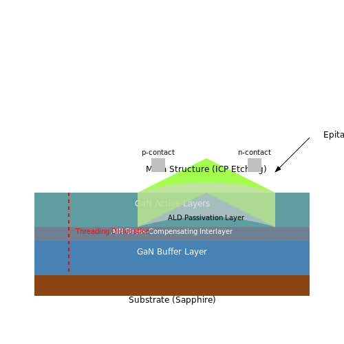
Epitaxial growth is the foundational step in Micro-LED fabrication, determining the crystalline quality, defect density, and ultimately the optoelectronic performance of the device. The process involves depositing single-crystal semiconductor layers (typically III-nitrides like GaN) on a substrate with matching lattice parameters to minimize strain-induced defects.
Metal-Organic Chemical Vapor Deposition (MOCVD)
The dominant technique for Micro-LED epitaxy is MOCVD, which leverages metal-organic precursors (e.g., trimethylgallium, TMGa) and ammonia (NH3) in a high-temperature (900–1100°C) reactor. The growth kinetics are governed by surface reaction rates and mass transport, described by the boundary layer model:
where dh/dt is the growth rate, ks is the surface reaction rate constant, Cg is the gas-phase concentration, and Ce is the equilibrium concentration at the surface. For GaN, typical growth rates range from 1–3 µm/hr, with V/III ratios (NH3/TMGa) exceeding 1000 to ensure stoichiometry.
Wafer-Level Challenges
Key challenges in epitaxial growth for Micro-LEDs include:
- Dislocation density: Threading dislocations (>108 cm−2 in conventional GaN-on-sapphire) act as non-radiative recombination centers. Techniques like epitaxial lateral overgrowth (ELO) reduce this to <106 cm−2.
- Wafer bowing: Thermal mismatch between GaN and substrates (e.g., Si, sapphire) induces stress, leading to cracking. Stress-compensating interlayers (AlN/GaN superlattices) are often employed.
- Doping uniformity: Precise control of Si (n-type) and Mg (p-type) doping is critical for carrier injection efficiency, with typical concentrations of 5×1018 cm−3 for n-GaN and 1×1019 cm−3 for p-GaN.
Wafer Processing Steps
Post-epitaxy, wafers undergo several critical processing stages:
- Photolithography: Patterning of Micro-LED mesas (5–50 µm) using deep-UV or electron-beam lithography.
- Dry etching: Inductively coupled plasma (ICP) etching with Cl2/BCl3 chemistries achieves vertical sidewalls (aspect ratios >5:1).
- Passivation: Atomic layer deposition (ALD) of Al2O3 or SiO2 mitigates surface recombination.
- Metallization: Sputtered Ti/Al/Ni/Au (n-contact) and Ni/Au (p-contact) stacks ensure ohmic behavior with specific contact resistances <10−4 Ω·cm2.
Thermal Considerations
Thermal resistance (Rth) of the epitaxial stack impacts junction temperature and efficiency droop. For a GaN-on-sapphire structure:
where ti is layer thickness, κi is thermal conductivity (e.g., 130 W/m·K for GaN), and A is the active area. Advanced substrates like GaN-on-SiC reduce Rth by 40% compared to sapphire.
2.2 Mass Transfer Techniques
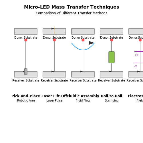
Mass transfer is a critical step in Micro-LED manufacturing, enabling the assembly of millions of microscopic LEDs onto a target substrate with high precision. The process involves detaching Micro-LEDs from their native growth substrate and transferring them to a display backplane. Several advanced techniques have been developed to achieve this at scale.
Pick-and-Place Transfer
Pick-and-place transfer employs robotic systems with micro-grippers or elastomer stamps to selectively pick individual Micro-LEDs and place them onto the target substrate. The placement accuracy is governed by:
where Δx is the total placement error, σmech is mechanical stage uncertainty, and σvision is alignment error from machine vision. Modern systems achieve ±1.5 µm precision but face throughput limitations (~10,000 units/hour).
Laser-Induced Forward Transfer (LIFT)
LIFT uses pulsed lasers to propel Micro-LEDs from a donor substrate to a receiver. A sacrificial absorption layer (e.g., polyimide) is irradiated, generating localized gas expansion that ejects the LED. The kinetic energy Ek of a transferred die is:
where ρ is material density, V is die volume, and v is ejection velocity. LIFT enables 106 transfers/hour but requires careful control of laser fluence to avoid thermal damage.
Fluidic Self-Assembly
This technique exploits fluid dynamics to align Micro-LEDs into pre-patterned receptor sites. The assembly yield depends on the probability P of a die finding a matching site:
where λ is the ratio of die concentration to site density. Hydrophobic/hydrophilic surface treatments improve alignment accuracy to 99.9% for sub-10 µm LEDs.
Roll-to-Roll Transfer
Roll-based methods use flexible intermediate carriers (e.g., PDMS stamps) to transfer Micro-LEDs in a continuous process. The peel-off adhesion energy γ must satisfy:
Recent advances in viscoelastic stamp materials enable transfer yields exceeding 99.5% at speeds of 0.5 m/s.
Electrostatic Transfer
This approach applies controlled electrostatic forces to selectively pick and place Micro-LEDs. The required electrode voltage V is derived from:
where F is detachment force, d is dielectric thickness, ϵ0 is permittivity, and A is contact area. Current systems achieve 500 nm placement accuracy with minimal mechanical stress.
Each technique presents trade-offs between throughput, precision, and compatibility with different LED sizes (5-100 µm). Hybrid approaches combining fluidic alignment with robotic fine-tuning are emerging as promising solutions for volume production.
2.3 Challenges in Micro-LED Production
Mass Transfer and Yield Issues
The most critical bottleneck in Micro-LED manufacturing is the mass transfer of individual LED chips (typically <50 µm) from a growth substrate to a display backplane. The required placement precision is <±1 µm, with defect rates needing to be below 0.0001% for commercial viability. Current pick-and-place techniques achieve only ~99.9% yield, translating to ~1,000 defective pixels in a 4K display. Fluidic self-assembly and elastomer stamp transfer show promise but struggle with throughput above 10 million units/hour.
Epitaxial Uniformity
Wavelength uniformity across wafers must be <±2 nm for color-critical applications. For a 200 mm GaN-on-sapphire wafer, this requires controlling:
where ΔT < 5°C and ΔP < 0.1 atm during MOCVD growth. The standard deviation of peak emission wavelength currently averages 4.7 nm in production environments.
Current Spreading in Microscale Devices
As LED sizes shrink below 20 µm, current crowding effects dominate. The current density J(r) follows:
where Ls is the current spreading length (~5 µm for standard p-GaN). This leads to non-uniform luminance and localized heating. Transparent conductive oxides (TCOs) with sheet resistance <10 Ω/sq are required but degrade at high current densities (>50 A/cm²).
Color Conversion Challenges
For RGB-less architectures using blue Micro-LEDs with quantum dot (QD) color converters, the photon conversion efficiency must exceed:
Current Cd-free QDs achieve only 72% efficiency with 10,000-hour lifetime at 10⁴ cd/m² brightness. Nanophosphor alternatives suffer from reabsorption losses >15%.
Thermal Management at High Density
A 1,000 ppi Micro-LED array operating at 10⁴ nits generates heat flux exceeding 500 W/cm². The thermal resistance Rth must satisfy:
where Tj is junction temperature and Ts is heatsink temperature. Conventional flip-chip bonding achieves only 5 K/W, necessitating monolithic integration with silicon drivers.
Backplane Integration
Active matrix backplanes require <2% threshold voltage variation in thin-film transistors (TFTs) when driving Micro-LEDs at <1 µA current levels. Low-temperature poly-Si (LTPS) achieves 1.5% uniformity but limits substrate size to Gen 6 (1500×1850 mm). Oxide TFTs scale to Gen 8.5 but exhibit 3-5% non-uniformity.
3. Consumer Electronics (Smartphones, TVs, Wearables)
3.1 Consumer Electronics (Smartphones, TVs, Wearables)
Pixel Density and Brightness Optimization
Micro-LED displays achieve pixel densities exceeding 2000 PPI through sub-10µm pixel pitches, enabled by monolithic integration or mass transfer techniques. The luminance L of a Micro-LED pixel is governed by:
where ηEQE is the external quantum efficiency, J the current density (A/cm²), and λ the emission wavelength. For smartphone displays, typical J values range from 10–50 A/cm² to maintain L > 1000 nits while minimizing Joule heating.
Power Efficiency in Wearables
Micro-LEDs in smartwatches leverage ultra-low threshold currents (≈0.1 mA at 2V) due to their small active areas (<50µm²). The power dissipation Pd scales with:
where Vth is the turn-on voltage (~1.8V for InGaN-based blue Micro-LEDs). This enables always-on displays with <1mW power draw for 1-inch panels.
Color Conversion Architectures
Full-color Micro-LED TVs use hybrid approaches:
- Direct-emission RGB: Individual InGaN (blue/green) and AlInGaP (red) Micro-LEDs with <5nm wavelength uniformity
- Quantum dot conversion: Blue Micro-LEDs with CdSe/Perovskite QD films (FWHM <30nm) achieving 140% NTSC color gamut
The color purity C is quantified by:
where P(λ) is the spectral power within the target wavelength band.
Active Matrix Backplane Integration
Micro-LED TVs utilize low-temperature poly-Si (LTPS) or oxide TFT backplanes with mobility >10 cm²/V·s to address 8K resolutions. The pixel charging time τ must satisfy:
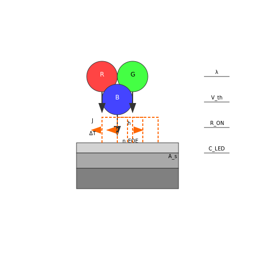
where N is the row count (7680 for 8K) and frefresh the frame rate (120Hz). This demands TFT RON < 100 kΩ for CLED ≈1pF.
Thermal Management in Smartphones
Micro-LED arrays in smartphones face thermal challenges due to I²R losses at high brightness. The temperature rise ΔT follows:
where h is the heat transfer coefficient (≈100 W/m²K for passive cooling) and As the substrate area. Advanced packages use copper-filled TSVs with thermal conductivity >400 W/mK to limit ΔT < 20°C at 2000 nits.
Augmented and Virtual Reality (AR/VR)
Optical Performance Requirements
Micro-LED displays for AR/VR demand exceptional optical characteristics to meet human visual acuity. The angular resolution of the human eye is approximately 1 arcminute, requiring pixel densities exceeding 3000 pixels per inch (PPI) for near-eye displays. The luminance requirement varies significantly between AR (≥ 5000 nits for outdoor visibility) and VR (100-200 nits for controlled lighting).
Where Np is the pixel count and Deye is the display-to-eye distance in millimeters. For a 120° field-of-view headset at 20mm eye relief, this necessitates ≥ 8K resolution per eye.
Efficiency Challenges
Current micro-LEDs face quantum efficiency roll-off at sub-10µm pixel sizes due to:
- Sidewall non-radiative recombination
- Current crowding effects
- Light extraction limitations
The external quantum efficiency (EQE) follows:
Where injection efficiency (ηinj) dominates at micro scales. Recent flip-chip designs with distributed Bragg reflectors (DBRs) have achieved 15-20% EQE at 5µm pixel sizes.
Color Conversion Techniques
Full-color micro-LED displays employ three primary methods:
| Method | Advantages | Challenges |
|---|---|---|
| RGB monolithic | High efficiency, precise alignment | Complex epitaxial growth |
| Quantum dot conversion | Wide color gamut (≥140% NTSC) | Photodegradation |
| Wavelength-selective filters | Stable performance | Optical losses (>60%) |
System Integration
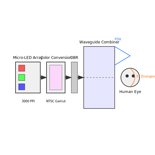
AR waveguide combiners impose additional constraints on micro-LED output characteristics:
- Collimation requirements: < 5° divergence
- Polarization control for diffraction efficiency
- Etendue matching with pupil expanders
Recent prototypes from Plessey and JBD demonstrate monolithic GaN-on-silicon micro-LED arrays with 0.3° beam divergence achieved through integrated microlens arrays.
Latency Considerations
Motion-to-photon latency below 20ms is critical for VR applications to prevent simulator sickness. Micro-LEDs enable sub-0.1ms response times, but system latency is dominated by:
Active matrix addressing with parallel data loading (e.g., 32-channel drivers) reduces τdrive to <1ms for 4K resolution at 120Hz refresh rates.
3.3 Automotive and Head-Up Displays (HUDs)
Optical Requirements for Automotive Micro-LED Displays
The integration of Micro-LEDs into automotive displays demands stringent optical performance metrics. Unlike consumer electronics, automotive displays must operate under extreme ambient lighting conditions, ranging from direct sunlight to low-light nighttime driving. The luminance requirement for automotive HUDs typically exceeds 10,000 cd/m² to ensure visibility in all scenarios. This is derived from the contrast ratio C needed for legibility:
where Ldisplay is the display luminance and Lambient is the ambient luminance. For sunlight conditions (Lambient ≈ 100,000 cd/m²), a contrast ratio of at least 1.1 necessitates Ldisplay ≥ 10,000 cd/m².
Thermal and Power Efficiency Challenges
Micro-LEDs are uniquely suited for automotive applications due to their high efficiency, but thermal management remains critical. The power dissipation P of a Micro-LED array is given by:
where N is the number of pixels, IF is forward current, VF is forward voltage, and Ileak accounts for leakage current. At high brightness, passive cooling becomes insufficient, necessitating active thermal management strategies such as integrated heat sinks or thermoelectric coolers.
Augmented Reality HUDs and Beam Steering
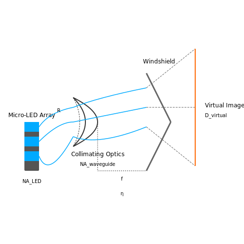
Advanced HUDs project virtual images onto the windshield using beam-steering optics. The virtual image distance Dvirtual is determined by the optical system's focal length f and the windshield curvature:
where R is the windshield radius of curvature and d is the projection distance. Micro-LEDs enable compact, high-resolution light engines for such systems, with pixel pitches below 10 µm to avoid visible granularity at short focal lengths.
Reliability and Automotive Qualification
Automotive displays must meet AEC-Q102 qualification standards, requiring operation over -40°C to +105°C with a lifetime exceeding 15,000 hours. Micro-LEDs exhibit superior reliability compared to OLEDs due to their inorganic nature, but package-level stresses (e.g., thermal cycling) can induce failure modes such as:
- Interconnect delamination due to coefficient of thermal expansion (CTE) mismatch
- Phosphor degradation under high-temperature operation
- Electromigration in fine-pitch bonding interconnects
Accelerated life testing models like the Arrhenius equation predict failure rates:
where A is a material constant, Ea is activation energy, and T is junction temperature.
Case Study: Collimating Optics for HUD Light Guides
Modern waveguide-based HUDs use Micro-LED arrays coupled into thin-film collimators. The collimation efficiency η depends on the numerical aperture (NA) matching between the LED and waveguide:
Typical values are NALED ≈ 0.3 (Lambertian emitter) and NAwaveguide ≈ 0.1, yielding η ≈ 11%. Micro-lens arrays or photonic crystal structures can improve this by reshaping the emission profile.
4. Efficiency and Brightness Improvements
4.1 Efficiency and Brightness Improvements
Quantum Efficiency and Light Extraction
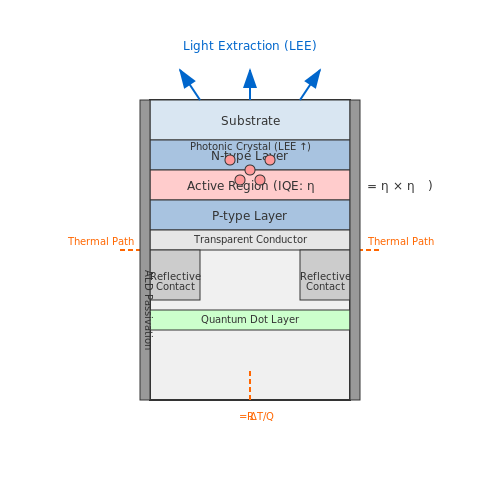
The internal quantum efficiency (IQE) of Micro-LEDs is fundamentally governed by radiative recombination rates in the active region. For a direct-bandgap semiconductor like GaN, the IQE (ηIQE) is expressed as:
where A, B, and C are Shockley-Read-Hall, radiative, and Auger recombination coefficients, respectively, and n is the carrier density. Modern Micro-LEDs achieve IQE >90% at low current densities (<1 A/cm²), but efficiency droop occurs at higher currents due to Auger recombination.
Light extraction efficiency (LEE) is improved through:
- Photonic crystal structures to redirect trapped waveguide modes.
- Sidewall passivation with atomic layer deposition (ALD) to reduce non-radiative surface recombination.
- Reflective contacts (e.g., Ag/Al) to recycle downward-emitted photons.
Current Density Optimization
Micro-LED brightness scales with current density (J), but efficiency peaks at a critical value Jpeak. For a 10 µm pixel:
where d is the active layer thickness, ncrit is the critical carrier density (~2×10¹⁸ cm⁻³ for InGaN), and τrad is the radiative lifetime (~1 ns). Pulse-width modulation (PWM) is often used to maintain J near Jpeak while achieving high luminance.
Color Conversion and Efficiency
For full-color displays, blue Micro-LEDs with quantum dot (QD) color converters achieve higher efficiency than RGB sub-pixels. The overall efficiency (ηsystem) combines:
where ηQD is the QD photoluminescence quantum yield (PLQY >95% in Cd-free QDs) and ηCF is the color filter transmission (~70%). Narrow-band QDs (FWHM <30 nm) improve color gamut to >110% NTSC.
Thermal Management
Joule heating at high currents (P = I²R) reduces efficiency. Thermal resistance (Rth) for a Micro-LED array is modeled as:
where tsub is substrate thickness, ksub is thermal conductivity (e.g., 130 W/m·K for sapphire), and Rinterface accounts for bonding layers. Active cooling with microfluidic channels or graphene heat spreaders maintains ΔT < 50°C at 10⁴ cd/m².
Practical Implementations
Samsung’s 2023 0.49" Micro-LED prototype achieved 1,000,000 nits brightness at 34% wall-plug efficiency using:
- Flip-chip bonding to reduce series resistance (<0.5 Ω).
- Black matrix isolation to minimize optical crosstalk.
- Hybrid driving circuits combining PWM and analog current control.
4.2 Flexible and Transparent Micro-LEDs
Mechanical and Optical Properties
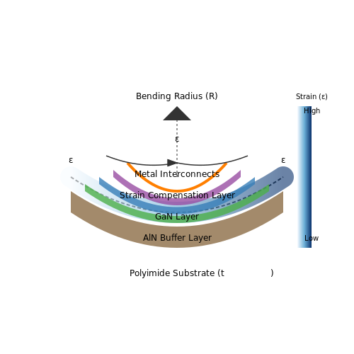
Flexible Micro-LEDs rely on deformable substrates such as polyimide (PI), polyethylene terephthalate (PET), or ultrathin glass (UTG). The critical parameter governing flexibility is the bending radius R, which must satisfy:
where Es is the substrate's Young's modulus, ts is its thickness, and σf is the fracture stress of the Micro-LED material. For GaN-based LEDs on polyimide, typical bending radii exceed 5 mm to prevent crack propagation.
Transparency is achieved by minimizing the opaque components (e.g., metal interconnects) and using transparent conductive oxides (TCOs) like indium tin oxide (ITO) or graphene. The optical transmittance T follows:
where α is the absorption coefficient and d is the thickness of the active layers. A typical transparent Micro-LED array achieves >80% transmittance in the visible spectrum.
Fabrication Techniques
Key fabrication approaches include:
- Transfer Printing: Micro-LEDs are epitaxially grown on a sacrificial substrate (e.g., sapphire) and transferred via elastomer stamps to flexible carriers.
- Laser Lift-Off (LLO): A pulsed laser separates the GaN layer from the growth substrate, enabling bonding to flexible backplanes.
- Monolithic Integration: Thin-film transistors (TFTs) are directly fabricated on flexible substrates alongside Micro-LEDs using low-temperature processes.
Challenges and Mitigation Strategies
Strain-Induced Performance Degradation
Bending induces strain in the active region, altering the bandgap and quantum efficiency. The strain ε is approximated by:
where tLED is the LED thickness. Strain compensation layers (e.g., AlN buffers) and neutral stress designs are employed to mitigate efficiency droop.
Interconnect Reliability
Repeated flexing causes metal trace fatigue. Solutions include:
- Mesh-patterned TCO interconnects to distribute stress.
- Embedded silver nanowires for high conductivity and flexibility.
Applications
Flexible and transparent Micro-LEDs enable:
- Wearable Displays: Curved smartwatches and foldable AR/VR headsets.
- Heads-Up Displays (HUDs): Transparent windshields with augmented reality overlays.
- Biomedical Sensors: Conformable epidermal phototherapy patches.
4.3 Integration with Quantum Dot Technology
Fundamental Principles of Quantum Dot Enhancement
Quantum dots (QDs) are semiconductor nanocrystals with tunable bandgaps, enabling precise control over emitted wavelengths based on their size. When integrated with Micro-LEDs, QDs act as wavelength converters, absorbing the high-energy blue or UV emission from the LED and re-emitting in a narrower spectral band. The Förster resonance energy transfer (FRET) efficiency between the Micro-LED and QDs is governed by:
where r is the donor-acceptor distance and R0 is the Förster radius. Optimizing this distance is critical for minimizing Stokes losses and maximizing color conversion efficiency.
Hybrid Micro-LED/QD Architectures
Two primary integration methods dominate:
- On-Chip QD Deposition: QDs are directly patterned onto the Micro-LED array using inkjet printing or photolithography. This approach minimizes optical crosstalk but requires robust QD stability under high current density (>100 A/cm²).
- Remote Phosphor Configuration: QDs are embedded in a separate film above the Micro-LED backplane. While thermally more stable, this method introduces additional optical interfaces, reducing light extraction efficiency by ~15–20%.
Challenges in QD-Micro-LED Integration
The primary limitations include:
- Thermal Degradation: At junction temperatures exceeding 80°C, QD photoluminescence quantum yield (PLQY) drops nonlinearly. Empirical data shows a PLQY reduction following:
where T0 is the characteristic thermal decay constant (typically 50–70 K for Cd-free QDs).
- Oxidation and Moisture Sensitivity: Perovskite QDs, despite high PLQY (>90%), degrade rapidly in ambient conditions. Encapsulation with atomic layer deposition (ALD) of Al2O3 improves lifetime to >10,000 hours at 85°C/85% RH.
Case Study: Full-Color Micro-LED Displays
Samsung's 2023 0.49-inch 4K Micro-LED prototype employs blue Micro-LEDs with red/green QDs, achieving 150% NTSC color gamut. Key metrics:
- Peak luminance: 1,000,000 nits (10× OLED)
- EQE (external quantum efficiency): 12.7% for green QD-converted pixels
- Pixel pitch: 4.8 µm, enabled by <1 µm QD patterning accuracy
Emerging Techniques
Recent advances include:
- Colloidal QD Electroluminescence: Direct QD-LEDs with Micro-LED-driven anodes eliminate Stokes losses. Progress in hole transport layers (HTLs) like NiOx has pushed external quantum efficiency to 18.2% (Nature Photonics, 2023).
- Nanophotonic Color Routing: Metasurfaces redirect blue Micro-LED light to adjacent QDs, enabling sub-micron pixel sizes without crosstalk (Science Advances, 2024).
The integration of Micro-LEDs with quantum dots represents a paradigm shift in display technology, combining the longevity and brightness of inorganic LEDs with the color precision of nanocrystals. Ongoing research focuses on improving thermal stability and manufacturability for consumer-scale adoption.
5. Key Research Papers and Journals
5.1 Key Research Papers and Journals
- Research Progress of Micro-LED Display Technology - MDPI — Micro-LED display technology is considered to be the next generation of display technology, which has the characteristics of high miniaturization, thin film and integration, as well as the advantages of high brightness, high contrast, fast response speed and long service life. However, in the development of Micro-LED display technology, there are still some technical and cost problems to be ...
- Recent Progress in Micro-LED-Based Display Technologies — In the same year, PlayNitride stepped in toward micro-LED-based display technology by introducing 0.89 in. 64 × 64 panels (105 pixels per inch) and another 3.12 in. 256 × 256 panels (116 pixels per inch) full-color display. ... The advantage of this approach is that the same method is used to pick up the thin-film transistor (electronic ...
- 5.1: A Novel PAM-PWM Hybrid Driving Method for Micro-LED Displays — The traditional PAM driving method is not suitable for micro-LED displays... Skip to Article Content; Skip to Article Information ... Journals. Journal of the Society for Information Display ... .org; SID Symposium Digest of Technical Papers. Volume 53, Issue S1 p. 66-68. Technical Sessions: Session 5: Display Driving Technology (Display ...
- High-performance thin-film transistors based on aligned carbon ... — An array of backplane transistors, responsible for switching and driving the individual display pixels, are required to control mLED/μLED displays [14].High current of 10 2 -10 6 mA/cm 2 is needed to drive mLEDs/μLEDs for light emission with luminance of 10 3 -10 7 cd/m 2 [15].There are currently two categories of materials used to drive mLED/μLED displays.
- Full-Color Realization of Micro-LED Displays - PMC — Mini-LEDs and micro-LEDs, which inherited the characteristics of inorganic LEDs and have micron-level dimensions, have become popular as the next generation of display technology. Micro-LED technology was first proposed by a research team at Texas Tech University in 2000 .
- Exploring Strategies for Performance Enhancement in Micro‐LEDs: a ... — Inorganic micro light-emitting diodes (Micro-LEDs) have emerged as a cutting-edge display technology that employs micronic LEDs as individual pixels in display panels. [ 1 - 5 ] It has various advantages over traditional technologies such as Liquid Crystal Display (LCD) and Organic Light-Emitting Diode (OLED).
- PDF Research Progress of Micro-LED Display Technology — the development of Micro-LED display technology, there are still some technical and cost problems to be solved. This paper focuses on the key technologies involved in Micro-LED display technology ...
- MicroLED technologies and applications: characteristics, fabrication ... — Micro light-emitting diode (microLED) technology is expected to be used in next-generation displays and other applications due to its many advantages. This paper categorizes, reviews, and analyzes the main challenges and technical solutions in the microLED displays manufacturing process, covering epitaxial growth, wafer fabrication, mass ...
- Flexible Micro-LEDs: Advanced Fabrication Techniques and ... - Springer — Flexible micro light-emitting diodes (micro-LEDs) have garnered significant attention due to their exceptional properties, including high luminance, energy efficiency, and mechanical robustness, positioning them as a promising technology for next-generation displays and electronic devices. As the Internet of Things (IoT) paradigm advances, the demand for portable and adaptable devices has led ...
5.2 Industry Reports and Whitepapers
- PDF A status of the MiniLEDs and MicroLEDs technology and market advancements — MicroLEDs technology and market advancements K-Display 2023 August 18, 2023 Yole Intelligence ... FIELDS OF EXPERTISE COVERING THE SEMICONDUCTOR INDUSTRY K-Display 2023 - MiniLEDs and MicroLEDs | www.yolegroup.com | @2023 4 ... • Display • Electronic Systems • Emerging Technologies. MicroLED Industry Momentum K-Display 2023 ...
- Global Market for Micro and Mini LEDs 2025-2035: MicroLED - GlobeNewswire — 2.2.5 High dynamic range Mini-LED displays 2.2.6 Quantum dot films for Mini-LED displays 2.2.7 Perovskite colour enhancement film in Mini-LEDs 2.2.8 Market map 2.2.9 Technology roadmap 2.3 Micro ...
- Global Mini-LED and Micro-LED Displays Market Report - GlobeNewswire — Related Links. The Global Market for Micro-LED Displays 2024-2034; 2023 MicroLED Displays Market Report - Global Industry Data, Analysis and Growth Forecasts by Type, Application and Region, 2022-2028
- Micro-LED Display Market Report: Trends, Forecast and Competitive ... — 4.5.1: ROW Micro-Led Display Market by Product: Large-scale Display, Small and Medium-sized Display, and Micro Display 4.5.2: ROW Micro-Led Display Market by End Use Industry: Consumer Electronics, Entertainment and Sports, Automotive, Retail, Government and Defence, and Others
- Micro-LED Displays Market Size, Share, Trends, Forecast 2030 — Micro-LED display technology is preferred by smartphone and tablet manufacturers because it improves user experience by providing better and enhanced picture quality. ... Micro-LED Displays Play a Vital Role in Consumer Electronics Industry Vertical. ... 5.2.1.5. Others 5.3. Europe Micro-LED Displays Market Outlook, by Industry Vertical, Value ...
- Micro-LED Display Market Size, Trends, Growth Report Forecast — The global micro-LED display market size was valued at USD 43.62 million in 2022 and is expected to reach USD 7.51 billion by 2028, growing at a CAGR of 135.88% ... Industry Analysis Report, Regional Outlook, Growth Potential, Price Trends, Competitive Market Share & Forecast 2023-2028. ... Rise in Adoption of Electronic Displays in Automotives
- Micro LED Display Market Growth Analysis - Technavio — Micro LED Display Market size is estimated to grow by USD 719567.1 million from 2024 to 2028 at a CAGR of 194.2% with the lease having the largest market size. Market Research Reports - Industry Analysis Size & Trends - Technavio ... Chart on Consumer electronics - Market size and forecast 2023-2028 ($ million)
- Micro-LED Market Research Analysis & Forecast | BIS Research — Industry report; Electronics-semiconductor ... 4.2.5.2 Canada ... In terms of application, the market is divided into display and lighting categories. Within the display segment, Micro-LED technology is used in various devices, including Near-to-Eye (NTE) devices like augmented reality (AR) and virtual reality (VR) headsets, where its high ...
- MicroLED Market Size, Share, Trends, Market Growth, and Business ... — The Asia-Pacific (APAC) region holds the largest share of the Micro-LED market, driven by strong demand from countries like South Korea, Japan, and China. This region is a hub for display technology innovation and manufacturing, with companies like Samsung and LG leading advancements in Micro-LED displays.
- Worldwide MicroLED Displays Industry to 2026 Key Trends and - GlobeNewswire — Contact Data CONTACT: ResearchAndMarkets.com Laura Wood, Senior Press Manager [email protected] For E.S.T Office Hours Call 1-917-300-0470 For U.S./CAN Toll Free Call 1-800-526-8630 For ...
5.3 Recommended Books and Online Resources
- ARTECH HOUSE USA : MicroLED Devices and Systems — 5. MicroLED Display System 5.1. Introduction 5.2. Battery Gap in Mobile Devices 5.3. MicroLED Display Power Calculations 5.4. Manufacturing of MicroLED Displays 5.5. Defect Management 5.6. References . 6 MicroLED Data Communication Systems 6.1 Introduction 6.2 Space Division Multiplexing (SDM) 6.3 System Design Framework 6.4 Potential System ...
- PDF Introduction to Microdisplays - download.e-bookshelf.de — 1.4.2 Matrix Addressed Displays 10 1.4.3 Field Emission Displays 11 1.4.4 Plasma Displays 11 1.4.5 Liquid Crystal Displays 12 1.4.6 Electroluminescent Displays 12 1.4.7 Electromechanical Displays 12 1.5 Microdisplay Evolution 13 1.6 Microdisplay Applications 15 1.6.1 Projection Displays 15 1.6.2 Near-to-Eye Displays 15
- Transfer Technology of Micro-LEDs for Display Applications — Part of the book series: Series in Display Science and Technology ((SDST)) ... The micro-LED display gets spot-light in this regard [2,3,4,5,6]. It has the highest brightness, durability, power efficiency, the fastest ... In 2020 IEEE 70th Electronic Components and Technology Conference (ECTC) (pp. 1031-1036) June 2020. (IEEE, 2020). Google ...
- PDF Laser‐Based Micro/Nano‐Processing Techniques for ... - LabXing — of Micro-LED display devices. 2. Overview of Micro-LED Displays and Laser- Material Interactions 2.1. Micro-LED Characteristics and Device Structures In simple terms, Micro-LEDs (2a) often refer to inorFigure-ganic, microscale light-emitting diodes, with a typical dimen-sion ranging from a few microns to a few tens of microns.[68]
- Advanced Mini-LED/Micro-LED Displays and Materials - MDPI — Micro-LED is a high-tech display technology. As the name implies, micro-LED displays consist of arrays of microscopic LEDs forming the individual pixel elements. ... e-Book format: Special Issues with more than 10 articles can be published as dedicated e-books, ensuring wide and rapid dissemination. Further information on MDPI's Special Issue ...
- PDF Transfer Technology of Micro-LEDs for Display Applications — micro-LED displays from their widespread utilization in our daily life. The biggest obstacle to the commercialization of micro-LED displays is cost-competitiveness [5, 6]. First, we need to consider the chip cost. A 4 K UHD display requires 25 million micro-LED chips. Assuming that the chip cost is $0.001 per chip, the total LED cost of the 4 K ...
- Exploring Strategies for Performance Enhancement in Micro‐LEDs: a ... — Inorganic micro light-emitting diodes (Micro-LEDs) have emerged as a cutting-edge display technology that employs micronic LEDs as individual pixels in display panels. [ 1 - 5 ] It has various advantages over traditional technologies such as Liquid Crystal Display (LCD) and Organic Light-Emitting Diode (OLED).
- Flexible Micro-LEDs: Advanced Fabrication Techniques and ... - Springer — Flexible micro light-emitting diodes (micro-LEDs) have garnered significant attention due to their exceptional properties, including high luminance, energy efficiency, and mechanical robustness, positioning them as a promising technology for next-generation displays and electronic devices. As the Internet of Things (IoT) paradigm advances, the demand for portable and adaptable devices has led ...
- 1-2023-APL-LP micro-LEDs.pdf - ResearchGate — College of Materials Science and Opto-Electronic Technology, University of Chinese Academy of Sciences ... 3D micro-LED displays combine the characteristics of 3D display and the advantages of ...
- Digital Design 5th Edition M Morris Mano And Michael D Ciletti — Computers, Technology and Science; Music, Arts & Culture; News & Public Affairs; Spirituality & Religion; Podcasts; Radio News Archive; Images. Metropolitan Museum Cleveland Museum of Art. ... This is a complete e-book by Morris Mano and Michael Ciletti. Addeddate 2023-09-01 00:11:51 Identifier digital-design-5th-edition-m-morris-mano-and ...