Organic Light Emitting Diodes (OLEDs)
1. Basic Principles of OLED Operation
Basic Principles of OLED Operation
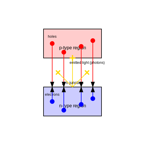
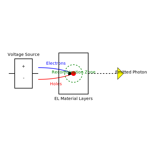
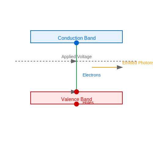
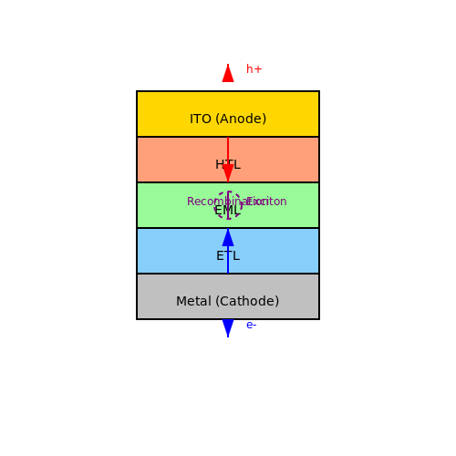
Organic Light Emitting Diodes (OLEDs) operate on the principle of electroluminescence in organic semiconductor materials. Unlike conventional LEDs, which rely on inorganic semiconductors like GaAs or InP, OLEDs utilize thin films of organic compounds that emit light when an electric current is applied. The fundamental mechanism involves the recombination of electron-hole pairs (excitons) within the emissive layer, resulting in photon emission.
Device Structure and Layers
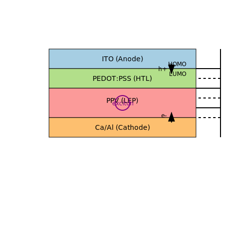
A typical OLED consists of the following layers, stacked between an anode and a cathode:
- Anode: Typically made of indium tin oxide (ITO), a transparent conductive material that injects holes into the organic layers.
- Hole Transport Layer (HTL): Facilitates the movement of holes from the anode to the emissive layer.
- Emissive Layer (EML): Composed of organic molecules or polymers where recombination occurs, leading to light emission.
- Electron Transport Layer (ETL): Transports electrons from the cathode to the emissive layer.
- Cathode: Often a low-work-function metal (e.g., aluminum or calcium) that injects electrons.
Charge Injection and Transport
When a voltage is applied across the OLED, charge carriers are injected from the electrodes:
where J is the current density, J0 is the saturation current density, q is the electron charge, V is the applied voltage, n is the ideality factor, k is Boltzmann's constant, and T is the temperature.
Holes from the anode and electrons from the cathode migrate toward the emissive layer through the respective transport layers. The efficiency of this process depends on the energy level alignment between layers, described by the highest occupied molecular orbital (HOMO) and lowest unoccupied molecular orbital (LUMO) levels.
Exciton Formation and Light Emission
When electrons and holes meet in the emissive layer, they form bound electron-hole pairs called excitons. These excitons can be in singlet or triplet states, with a statistical distribution of 25% singlets and 75% triplets in non-phosphorescent materials. The radiative decay of singlet excitons produces fluorescence, while triplet excitons typically undergo non-radiative decay unless the material is phosphorescent.
where ηEQE is the external quantum efficiency, γ is the charge balance factor, ηr is the radiative exciton fraction, and φPL is the photoluminescence quantum yield.
Color Generation and Efficiency
OLEDs can emit different colors by varying the organic materials in the emissive layer. Common approaches include:
- Small-molecule OLEDs (SM-OLEDs): Use evaporated organic dyes with precise color tuning.
- Polymer OLEDs (PLEDs): Employ conjugated polymers for solution-processable devices.
- Phosphorescent OLEDs (PHOLEDs): Utilize heavy-metal complexes to harvest both singlet and triplet excitons, achieving near 100% internal quantum efficiency.
The power efficiency of an OLED is given by:
where ħω is the photon energy and V is the operating voltage.
Degradation Mechanisms
OLED performance degrades over time due to several factors:
- Electrochemical reactions: Between the organic layers and electrodes.
- Morphological changes: Crystallization or phase separation in the organic films.
- Exciton-polaron quenching: High current densities lead to exciton-exciton annihilation.
1.2 Comparison with Traditional LEDs and LCDs
Structural and Operational Differences
Traditional Light Emitting Diodes (LEDs) rely on inorganic semiconductors such as gallium nitride (GaN) or gallium arsenide (GaAs), where electron-hole recombination in the p-n junction produces light. In contrast, Organic Light Emitting Diodes (OLEDs) utilize organic emissive layers (e.g., small molecules or polymers) that emit light via electroluminescence when excited by an electric field. Unlike LEDs, OLEDs do not require a backlight, as each pixel is self-emissive.
Liquid Crystal Displays (LCDs) operate on an entirely different principle: they modulate light from a backlight (often LED-based) using liquid crystals that twist in response to an electric field. This modulation, combined with color filters, produces the displayed image. LCDs are inherently transmissive, whereas OLEDs are emissive, leading to fundamental differences in contrast ratios, viewing angles, and power efficiency.
Performance Metrics
Efficiency and Power Consumption
The luminous efficacy of OLEDs is given by:
where ηext is the external quantum efficiency, γ represents the charge balance factor, ηint is the internal quantum efficiency, and ηout accounts for light outcoupling efficiency. OLEDs typically achieve ηext values of 20-30%, while inorganic LEDs can exceed 80% due to superior charge carrier mobility and radiative recombination rates.
LCDs suffer from efficiency losses due to the absorption of light by color filters and polarizers, with typical optical efficiency around 5-10%. OLEDs, being self-emissive, avoid these losses but face challenges in achieving high brightness at low drive voltages.
Contrast Ratio and Black Levels
OLEDs exhibit theoretically infinite contrast ratios because individual pixels can be completely turned off, achieving true black. In contrast, LCDs rely on blocking the backlight, which often results in light leakage and limited contrast ratios (typically 1000:1 to 5000:1 for high-end displays).
Response Time and Refresh Rates
The response time of OLEDs is in the microsecond range (1-10 μs), making them suitable for high-frequency applications such as virtual reality (VR) and gaming displays. LCDs, limited by the relaxation time of liquid crystals, typically have response times in the millisecond range (2-8 ms), leading to motion blur in fast-moving scenes.
Flexibility and Form Factor
OLEDs can be fabricated on flexible substrates (e.g., polyimide), enabling bendable and foldable displays—an impossibility for rigid inorganic LEDs and LCDs. This flexibility has led to innovations in wearable technology and rollable screens.
Lifetime and Degradation
A major drawback of OLEDs is their susceptibility to degradation. The organic materials degrade over time, particularly blue emitters, leading to color shifts and reduced luminance. The operational lifetime (L50, time until brightness drops to 50% of initial value) for OLEDs is typically 10,000-50,000 hours, whereas inorganic LEDs can exceed 100,000 hours. LCDs, with no emissive decay mechanism, primarily suffer from backlight degradation.
Manufacturing and Cost Considerations
OLED production involves vacuum deposition or solution processing of organic layers, which is more complex and costly than the well-established fabrication of inorganic LEDs and LCDs. However, advancements in inkjet printing and roll-to-roll processing are reducing OLED manufacturing costs.
Applications and Market Trends
OLEDs dominate high-end consumer electronics (smartphones, TVs) due to their superior image quality, while LCDs remain prevalent in cost-sensitive applications. Micro-LEDs, an emerging technology, aim to combine the efficiency of inorganic LEDs with the pixel-level control of OLEDs, though manufacturing challenges persist.
1.3 Key Advantages of OLED Technology
Superior Contrast and True Blacks
Unlike liquid crystal displays (LCDs), which rely on a backlight, OLEDs are emissive devices where each pixel generates its own light. When a pixel is turned off, it emits no light, achieving an infinite contrast ratio and true blacks. This is quantified by the contrast ratio:
where \( L_{\text{min}} = 0 \) for OLEDs, making \( C \to \infty \). LCDs, due to backlight leakage, typically achieve \( C \approx 1000:1 \).
Wide Viewing Angles
OLEDs maintain color accuracy and brightness at viewing angles up to 84°, unlike LCDs, which suffer from gamma shift and luminance drop-off beyond 45°. The angular dependence of luminance \( L( heta) \) follows:
where \( n \approx 1.5 \) for OLEDs (Lambertian-like emission), compared to \( n \approx 2.5 \) for LCDs.
Flexible and Thin Form Factors
OLEDs can be fabricated on flexible substrates (e.g., polyimide) due to their all-organic structure. Thicknesses as low as 100–300 nm are achievable, enabling rollable displays and conformal integration. The bending radius \( R \) is governed by:
where \( E \) is Young’s modulus, \( t \) is thickness, and \( \sigma_y \) is yield strength. For typical OLEDs, \( R < 5 \) mm is feasible.
Fast Response Time
OLEDs exhibit sub-microsecond response times (\( \tau < 1 \) µs), as carrier recombination in organic semiconductors is inherently faster than liquid crystal reorientation (\( \tau \approx 1–10 \) ms in LCDs). This eliminates motion blur in high-refresh-rate applications (e.g., VR headsets).
Energy Efficiency
OLEDs consume power only for illuminated pixels. For dark scenes, energy savings exceed 40% compared to LCDs. The power dissipation \( P \) per pixel is:
where \( J \) is current density, \( V \) is operating voltage, \( A \) is pixel area, and \( \eta_{\text{EQE}} \) is external quantum efficiency (typically 20–30% for phosphorescent OLEDs).
Manufacturing Scalability
Solution-processable OLED materials enable inkjet printing and roll-to-roll fabrication, reducing production costs. Evaporation-based methods achieve pixel densities > 500 PPI for microdisplays.
2. Organic Semiconductor Materials
2.1 Organic Semiconductor Materials
Electronic Structure and Charge Transport
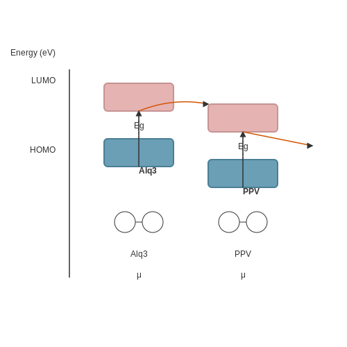
Organic semiconductors are characterized by a π-conjugated electron system, where delocalized π-electrons facilitate charge transport. The highest occupied molecular orbital (HOMO) and lowest unoccupied molecular orbital (LUMO) serve as analogs to the valence and conduction bands in inorganic semiconductors. The energy gap (Eg) between HOMO and LUMO determines the emission wavelength in OLEDs and is tunable via molecular design:
Charge carrier mobility (μ) in these materials is typically anisotropic and lower than in inorganic crystals due to localized hopping transport. For small molecules like tris(8-hydroxyquinolinato)aluminum (Alq3), mobility follows the Einstein relation:
where D is the diffusion coefficient, e is elementary charge, and kBT is thermal energy.
Material Classes and Functional Groups
Two primary categories dominate OLED applications:
- Small-molecule materials (e.g., Alq3, TPD): Processed via vacuum deposition, offering high purity and well-defined film morphology.
- Polymeric materials (e.g., PPV, F8BT): Solution-processable, enabling large-area fabrication through spin-coating or inkjet printing.
Key functional groups enhance performance:
- Electron-transport layers (ETLs) often incorporate oxadiazole or triazole moieties
- Hole-transport layers (HTLs) utilize triphenylamine derivatives
- Emissive materials employ iridium complexes (e.g., Ir(ppy)3) for phosphorescence
Degradation Mechanisms
Material stability is critical for operational lifetime. Major degradation pathways include:
- Electrochemical oxidation at the anode interface
- Exciton-polaron annihilation under high current density
- Crystallization of amorphous films during operation
The degradation rate follows a stretched exponential function:
where L0 is initial luminance, τ is characteristic lifetime, and β is dispersion parameter (typically 0.3–0.7).
Recent Advances in Molecular Design
Thermally activated delayed fluorescence (TADF) materials achieve near-100% internal quantum efficiency through reverse intersystem crossing (RISC). Key molecular designs include:
- Donor-acceptor architectures with small ΔEST (singlet-triplet gap)
- Multi-resonant structures for narrowband emission
- Host-guest systems with energy cascade alignment
2.2 Layer-by-Layer Structure of OLEDs
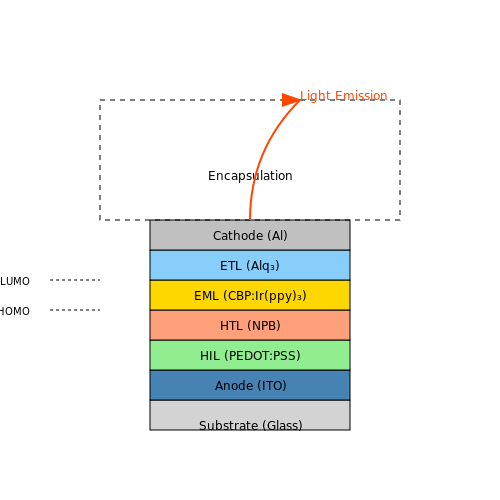
The functional architecture of an OLED is a carefully engineered stack of organic and inorganic layers, each serving a distinct role in charge injection, transport, recombination, and light emission. The precise arrangement and material selection determine the device's efficiency, lifetime, and spectral characteristics.
Substrate Layer
The substrate provides mechanical support and can be rigid (glass) or flexible (plastic, metal foil). For flexible OLEDs, a barrier coating is often applied to prevent moisture and oxygen ingress, which degrade organic materials. Common substrates include:
- Glass: High transparency (~92%) and thermal stability but brittle.
- Polyimide (PI): Flexible with a high glass transition temperature (Tg > 400°C).
- PEN/PET: Low-cost plastics with moderate barrier properties.
Anode Layer
The anode injects holes into the organic stack and must exhibit high work function (>4.7 eV) for efficient hole injection. Indium Tin Oxide (ITO) dominates due to its:
- Optical transparency (>85% in visible spectrum)
- Sheet resistance (10–20 Ω/sq for 100 nm thickness)
- Work function tunable via plasma treatment (4.7–5.2 eV)
Emerging alternatives include:
- Silver nanowires: Flexible with low sheet resistance (≤10 Ω/sq)
- Conductive polymers (PEDOT:PSS): Solution-processable but hygroscopic
Hole Injection Layer (HIL)
The HIL reduces the energy barrier between the anode and the Hole Transport Layer (HTL). Common materials include:
where ΔE is minimized using:
- MoO3: Work function ~6.9 eV, thermally evaporated
- HAT-CN: Electron-accepting molecule with deep LUMO (-5.7 eV)
Hole Transport Layer (HTL)
The HTL transports holes to the emission layer with high mobility (10-3–10-4 cm2/V·s). Key materials:
- NPB (N,N′-di(1-naphthyl)-N,N′-diphenyl-(1,1′-biphenyl)-4,4′-diamine): Mobility ~10-4 cm2/V·s
- Spiro-OMeTAD: Amorphous morphology prevents crystallization
Emission Layer (EML)
The EML hosts exciton recombination and light emission. It typically consists of:
- Host material: Wide energy gap (e.g., CBP, TCTA) transporting both carriers
- Dopant (1–10%): Fluorescent (e.g., Alq3) or phosphorescent (e.g., Ir(ppy)3) emitters
Doping follows Förster resonance energy transfer (FRET):
where R0 is the Förster radius and r is donor-acceptor distance.
Electron Transport Layer (ETL)
The ETL delivers electrons to the EML, requiring:
- High electron mobility: >10-3 cm2/V·s (e.g., TPBi, Bphen)
- Low LUMO level: Matching cathode work function
Cathode Layer
Low-work-function metals (<4.0 eV) enable efficient electron injection. Standard configurations:
- Bilayer: LiF (1 nm)/Al (100 nm) reduces injection barrier
- Alloy cathodes: Mg:Ag (10:1 ratio) for semi-transparent devices
Encapsulation
Thin-film encapsulation (TFE) using alternating inorganic (Al2O3, SiNx) and organic layers achieves water vapor transmission rates (WVTR) <10-6 g/m2/day.
2.3 Small Molecule vs. Polymer OLEDs
Structural and Material Differences
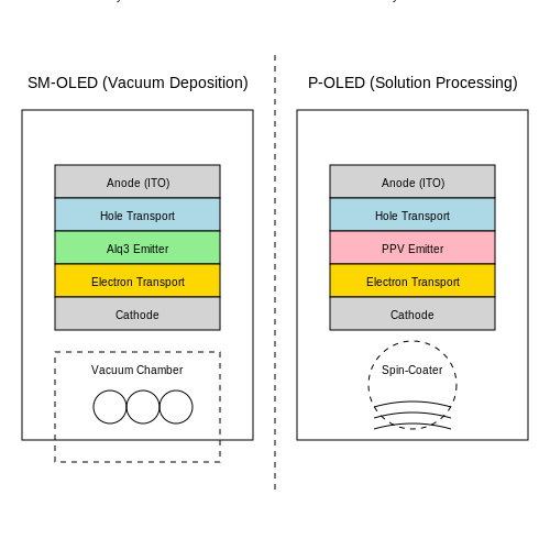
Small-molecule OLEDs (SM-OLEDs) utilize low-molecular-weight organic compounds, such as tris(8-hydroxyquinolinato)aluminum (Alq3), deposited via vacuum thermal evaporation. In contrast, polymer OLEDs (P-OLEDs) employ high-molecular-weight conjugated polymers like poly(p-phenylene vinylene) (PPV), processed through solution-based techniques such as spin-coating or inkjet printing. The molecular weight disparity leads to distinct film formation mechanisms: SM-OLEDs grow in a crystalline or amorphous thin-film state, while P-OLEDs form disordered polymer matrices.
Fabrication and Processing
SM-OLED fabrication requires high-vacuum deposition (<10-6 Torr) for precise layer-by-layer growth, enabling complex multilayer architectures. The process yields high-purity films with controlled thicknesses down to nanometer precision. P-OLEDs, however, leverage solution processability, allowing roll-to-roll manufacturing and large-area deposition. The trade-off lies in solvent compatibility constraints and the difficulty of achieving sharp heterojunctions in polymer blends.
Charge Transport and Efficiency
SM-OLEDs exhibit superior charge mobility (10-3–10-1 cm2/V·s) due to ordered molecular packing, enhancing recombination efficiency. P-OLEDs typically show lower mobility (10-5–10-3 cm2/V·s) because of chain entanglements and hopping-limited transport. However, recent developments in donor-acceptor copolymers have narrowed this gap, with some achieving >20% external quantum efficiency (EQE).
Lifetime and Degradation
SM-OLEDs demonstrate longer operational lifetimes (>100,000 hours for green emitters) due to stable molecular structures and encapsulation compatibility. P-OLEDs face faster degradation from oxygen and moisture permeation through pinholes in solution-processed films. Crosslinking strategies and nanoparticle doping have improved P-OLED stability, but they still lag behind SM-OLEDs in accelerated aging tests.
Applications and Commercialization
SM-OLEDs dominate high-end displays (e.g., Samsung QD-OLED TVs) where precision and longevity are critical. P-OLEDs find use in flexible electronics (e.g., LG Rollable TVs) and printed lighting panels, benefiting from their mechanical flexibility and scalable production. Emerging hybrid approaches combine SM-OLED emitters with polymer hosts to balance performance and processability.
Recent Advances
Thermally activated delayed fluorescence (TADF) SM-OLEDs now achieve near-100% internal efficiency through triplet harvesting. In P-OLEDs, non-fullerene acceptors in bulk heterojunctions have pushed power conversion efficiencies above 18% for white emission. Both technologies face ongoing challenges in blue emitter stability and cost-effective manufacturing at scale.
3. Vacuum Deposition Methods
3.1 Vacuum Deposition Methods
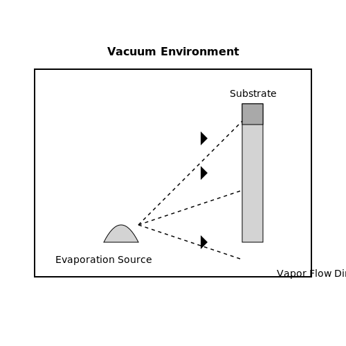
Vacuum deposition is the dominant technique for fabricating high-performance OLEDs, enabling precise control over layer thickness, purity, and uniformity. The process occurs in a high-vacuum environment (<10−6 Torr) to minimize contamination and ensure molecular-level precision.
Thermal Evaporation
Thermal evaporation involves heating organic materials in a crucible until they sublime, forming a vapor that condenses on a substrate. The deposition rate R is governed by the Knudsen equation:
where P is the vapor pressure, A is the orifice area, α is the sticking coefficient, M is the molecular weight, and T is the source temperature. Key advantages include:
- High purity: Minimal contamination due to vacuum conditions.
- Layer-by-layer control: Enables precise heterostructure fabrication.
- Material efficiency: Up to 80% utilization with proper shadow masking.
Organic Molecular Beam Deposition (OMBD)
A refined variant of thermal evaporation, OMBD employs ultra-high vacuum (<10−9 Torr) and in-situ monitoring (e.g., quartz crystal microbalances) to achieve monolayer accuracy. The mean free path λ of molecules is critical:
where d is the molecular diameter. OMBD is essential for:
- Dopant concentration control within ±1%.
- Sharp interfaces (<0.5 nm roughness) for tandem OLEDs.
Shadow Mask Patterning
Fine metal masks (FMMs) with <50 µm apertures align to substrates to deposit RGB subpixels. Alignment tolerances must be <5 µm to prevent color mixing. The mask-substrate gap g affects feature blurring:
where t is mask thickness, s is the source-mask distance, and d is the aperture size.
Challenges and Mitigations
- Material degradation: Thermal decomposition is minimized using low-temperature effusion cells.
- Uniformity: Planetary substrate holders ensure ±3% thickness variation across Gen 8.5 panels.
- Throughput: Linear sources and multi-crucible systems achieve 100 nm/sec deposition rates.
Recent advancements include hybrid deposition combining vacuum evaporation for organics with sputtering for electrodes, enabling flexible OLEDs with <100 µm bending radii.
3.2 Solution-Processable Techniques
Spin Coating
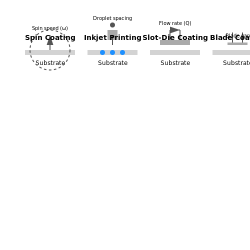
Spin coating is a widely adopted solution-processable technique for depositing organic semiconductor layers in OLEDs. The process involves dispensing a solution of the organic material onto a substrate, which is then rotated at high speeds (typically 1000–5000 rpm) to spread the solution uniformly via centrifugal force. The thickness d of the resulting film is governed by:
where k is a material-dependent constant, c is the solution concentration, and ω is the angular velocity. Spin coating offers excellent uniformity and reproducibility but suffers from material wastage, as over 90% of the solution is ejected during spinning.
Inkjet Printing
Inkjet printing enables precise patterning of OLED materials with micrometer-scale resolution, making it suitable for large-area and flexible displays. The technique relies on piezoelectric or thermal actuators to eject droplets (typically 10–100 picoliters) of the organic solution onto predefined pixel locations. Key parameters include:
- Drop spacing (5–50 µm) determines layer continuity.
- Solvent evaporation rate affects film morphology.
- Surface energy of the substrate controls droplet spreading.
Inkjet-printed OLEDs have achieved external quantum efficiencies (EQEs) exceeding 20% for green emitters, rivaling vacuum-deposited counterparts.
Slot-Die Coating
Slot-die coating is a roll-to-roll (R2R) compatible method for high-throughput fabrication of OLEDs. A precision pump delivers the organic solution through a slit-shaped die, forming a wet film on a moving substrate. The film thickness is given by:
where Q is the flow rate, v is the substrate velocity, and w is the coating width. Slot-die coating achieves ≤5% thickness variation over meter-scale areas, critical for industrial production.
Blade Coating
Blade coating, or knife-edge coating, uses a sharp blade to spread a solution reservoir across a substrate. The gap between the blade and substrate (10–200 µm) sets the wet film thickness. This method is particularly effective for viscous solutions (e.g., polymer-based emitters) and has enabled OLEDs with luminance >10,000 cd/m² at low driving voltages.
Material Considerations
Solution-processable OLED materials must satisfy:
- Solubility (>10 mg/mL in orthogonal solvents).
- Film-forming properties (low roughness, high homogeneity).
- Charge transport (hole/electron mobility >10⁻³ cm²/V·s).
Recent advances in molecular design, such as incorporating branched alkyl chains or polar side groups, have improved solubility without compromising optoelectronic performance.
Challenges and Mitigation Strategies
Solution processing introduces unique challenges compared to vacuum deposition:
| Challenge | Mitigation |
|---|---|
| Interlayer mixing | Orthogonal solvent systems |
| Film defects (pinholes) | Solvent additive engineering |
| Low-resolution patterning | Electrohydrodynamic printing |
For instance, adding 1% high-boiling-point solvent (e.g., 1-chloronaphthalene) to the emitting layer solution reduces crystallization-induced defects, enhancing device lifetime by 3×.
3.3 Challenges in Large-Scale Production
Material Uniformity and Deposition
The deposition of organic thin films in OLEDs requires atomic-level precision to ensure uniform electroluminescence across large panels. Small variations in layer thickness (e.g., ±5 nm) can lead to significant differences in charge carrier mobility and recombination efficiency. For instance, the luminance L of an OLED follows:
where ηint is internal quantum efficiency, ηout is outcoupling efficiency, J is current density, and q is elementary charge. Non-uniform deposition reduces ηint due to localized quenching sites.
Environmental Sensitivity
Organic materials degrade rapidly when exposed to moisture or oxygen. The oxidation rate R of common emissive layers like Alq3 follows Arrhenius kinetics:
where A is the pre-exponential factor, Ea is activation energy (~0.5 eV for Alq3), and kBT is thermal energy. This necessitates ultra-high vacuum (<10-6 Torr) deposition systems and hermetic encapsulation, increasing production costs.
Patterning Techniques
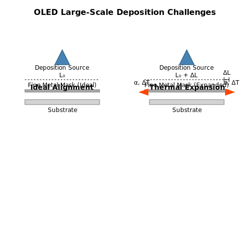
Fine Metal Mask (FMM) evaporation struggles with alignment accuracy below 5 μm for RGB subpixels. Shadow mask thermal expansion (ΔL) during deposition is given by:
where α is the coefficient of thermal expansion (~17 ppm/K for Invar alloys), L0 is initial mask dimension, and ΔT is temperature change. For 8th-generation (2200×2500 mm) substrates, this causes ~37 μm misalignment at ΔT=50°C.
Encapsulation Challenges
Thin-film encapsulation (TFE) using alternating inorganic/organic layers must achieve water vapor transmission rates (WVTR) below 10-6 g/m2/day. The defect density D in plasma-enhanced chemical vapor deposition (PECVD) SiNx films scales as:
where PRF is RF power, Ts is substrate temperature, and d is film thickness. Achieving <5 pinholes/cm2 requires sub-100 nm thickness control across meter-scale panels.
Cost Drivers
- Material utilization: Only 20-30% of evaporated organic materials deposit on the substrate in linear source systems
- Capital expenditure: Gen 8.5 OLED fabs require >$7 billion investment
- Yield loss: Particulate defects cause 15-20% yield loss in current production lines
Alternative Approaches
Solution-processable OLED materials promise lower costs but face tradeoffs in efficiency. The solubility parameter δ must match the solvent system:
where ΔHv is heat of vaporization, R is gas constant, T is temperature, and Vm is molar volume. Most high-efficiency phosphorescent emitters have δ > 23 MPa1/2, limiting solvent choices.
4. Efficiency and Luminance
4.1 Efficiency and Luminance
Fundamental Efficiency Metrics
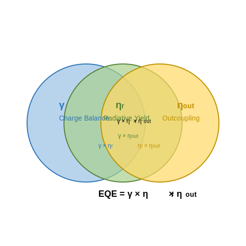
The performance of an OLED is quantified by three primary efficiency metrics: internal quantum efficiency (IQE), external quantum efficiency (EQE), and power efficiency (PE). Each measures distinct aspects of the device's electroluminescent conversion process.
IQE is limited by spin statistics, as only 25% of excitons formed are singlet states in fluorescent materials. Phosphorescent and thermally activated delayed fluorescence (TADF) emitters circumvent this by harvesting both singlet and triplet excitons, theoretically achieving 100% IQE.
Here, γ is the charge balance factor, ηr is the radiative exciton fraction, ϕPL is the photoluminescence quantum yield, and ηout is the outcoupling efficiency (typically 20-30% in planar OLEDs).
Luminance and Power Efficiency
Luminance (L), measured in candela per square meter (cd/m²), relates to the human eye's photopic response. The power efficiency (PE) in lumens per watt (lm/W) combines electrical and optical performance:
For a green OLED with L = 1,000 cd/m² at J = 10 mA/cm² and V = 4 V, PE ≈ 25 lm/W. Microcavity structures and light extraction techniques can enhance this by optimizing ηout.
Advanced Efficiency Optimization
State-of-the-art OLEDs employ:
- Doped transport layers to improve charge balance (γ → 1).
- High-quantum-yield emitters (e.g., iridium complexes with ϕPL > 90%).
- Scattering layers or corrugated substrates to boost outcoupling.
Luminance Degradation Mechanisms
Efficiency droop at high currents arises from:
- Polaron quenching (charge-induced exciton dissociation).
- Triplet-triplet annihilation (TTA) in phosphorescent systems.
- Joule heating reducing ϕPL.
Accelerated aging tests at 1,000 cd/m² show luminance half-life (L0/2) ranging from 10,000 hours (rigid OLEDs) to 1,000 hours (flexible variants).
4.2 Color Gamut and Reproduction
Fundamentals of Color Gamut in OLEDs
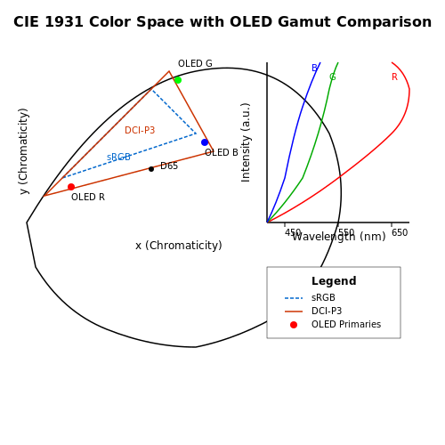
The color gamut of an OLED display defines the range of colors it can reproduce within a given color space, typically standardized as sRGB, Adobe RGB, or DCI-P3. Unlike traditional LCDs, which rely on color filters and backlighting, OLEDs generate light directly through electroluminescence in organic emissive layers. This intrinsic property allows for superior color purity and a wider gamut, as the emission spectra of organic molecules can be finely tuned.
The chromaticity coordinates of an OLED's primary colors (red, green, blue) determine the vertices of the gamut triangle in the CIE 1931 color space. The area enclosed by these points, relative to a reference gamut, quantifies the display's color coverage. For instance, a high-end OLED may achieve 95% of the DCI-P3 space, enabling cinematic color reproduction.
Color Reproduction and White Point Calibration
Accurate color reproduction requires precise control over the white point, typically targeting D65 (6504 K) for standard displays. In OLEDs, the white point is achieved by balancing the intensities of the RGB subpixels. The relationship between luminance and chromaticity is governed by the CIE tristimulus values:
where \(E(\lambda)\) is the spectral power distribution of the emitted light, and \(\bar{x}(\lambda)\), \(\bar{y}(\lambda)\), \(\bar{z}(\lambda)\) are the CIE color-matching functions. The white point is then derived from the normalized tristimulus values:
Challenges in Wide-Gamut OLED Design
While OLEDs inherently support wide gamuts, achieving consistent color reproduction across varying brightness levels remains a challenge due to the differential aging of organic materials (burn-in) and current-density-dependent spectral shifts. Advanced compensation algorithms, such as real-time feedback from optical sensors or lookup-table-based gamma correction, are employed to mitigate these effects.
Another critical factor is the color rendering index (CRI), which evaluates how naturally colors are rendered under the display's illumination. High-CRI OLEDs (>90) require carefully engineered emitter stacks with minimal spectral gaps, often incorporating additional dopants or hybrid phosphorescent/fluorescent systems.
Metamerism and Observer Variability
Metameric failure—where colors match under one illuminant but diverge under another—is a key consideration in OLED design. The narrow emission spectra of some organic emitters can exacerbate metamerism, necessitating multi-peak emitters or broadband phosphors. Additionally, observer variability (e.g., differences in human cone response) is accounted for by statistical modeling in color calibration pipelines.
Modern OLED manufacturing integrates spectrophotometers and ellipsometry tools to measure and adjust color parameters at the subpixel level, ensuring uniformity across panels. This is particularly critical for medical imaging and professional grading monitors, where ΔE < 1 (just-noticeable difference) is often required.
Applications in High-Fidelity Displays
The expanded gamut of OLEDs has enabled breakthroughs in consumer and professional markets. For example, Sony's BVM-HX310 mastering monitor achieves 100% coverage of both DCI-P3 and BT.2020 spaces, leveraging a custom tandem OLED structure with optimized carrier confinement. Similarly, smartphone displays now routinely exceed 100% sRGB, with Samsung's AMOLED panels using quantum dot color converters to enhance red and green saturation.
4.3 Lifespan and Degradation Factors
Intrinsic Degradation Mechanisms
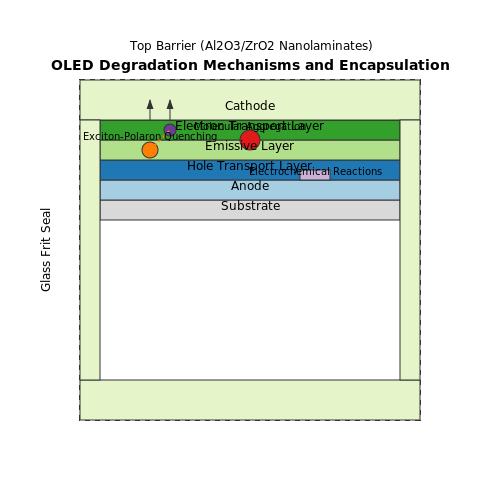
The operational lifetime of OLEDs is primarily limited by intrinsic chemical and physical degradation processes. Key mechanisms include:
- Electrochemical reactions at electrode-organic interfaces, leading to oxidation or reduction of organic layers.
- Exciton-polaron quenching, where high-energy excitons react with charge carriers, forming non-emissive species.
- Molecular aggregation and crystallization over time, disrupting charge transport and emission uniformity.
The degradation rate follows an Arrhenius temperature dependence:
where k is the degradation rate constant, A the pre-exponential factor, Ea the activation energy, and T the absolute temperature.
External Factors Affecting Lifetime
Current Density and Brightness
Luminance decay follows a power-law relationship with initial brightness:
where L0 is initial luminance, α and β are material-dependent coefficients. Operating at 1000 cd/m² typically yields lifetimes of 10,000–100,000 hours for modern phosphorescent OLEDs.
Environmental Conditions
Moisture and oxygen ingress through pinholes or edge seals cause irreversible damage:
- Water molecules react with cathode metals (e.g., calcium), increasing series resistance.
- Oxygen quenches excitons and forms carbonyl defects in emitting layers.
Accelerated Aging Tests
Standardized testing methods include:
| Test | Conditions | Lifetime Metric |
|---|---|---|
| Constant Current | Fixed current, elevated temperature (e.g., 85°C) | T50 (time to 50% luminance decay) |
| Cyclic Stress | Pulsed operation (e.g., 1 kHz, 50% duty cycle) | Number of cycles to failure |
Material-Specific Stability
Different emitter types exhibit distinct degradation pathways:
- Fluorescent emitters: Degrade primarily through singlet-triplet annihilation.
- Phosphorescent emitters: Suffer from triplet-polaron annihilation and ligand dissociation.
- TADF emitters: Exhibit degradation via reverse intersystem crossing-induced bond breaking.
Encapsulation Technologies
Effective barrier layers must achieve water vapor transmission rates (WVTR) below 10-6 g/m²/day. Advanced approaches include:
- Atomic layer deposition (ALD) of alternating Al2O3/ZrO2 nanolaminates
- Hybrid organic-inorganic coatings with self-healing properties
- Glass frit edge sealing with laser-assisted bonding
Operational Strategies for Lifetime Extension
System-level techniques to mitigate degradation:
where ΔV is the voltage rise due to aging, J is current density, and γ a device-specific parameter. Compensation methods include:
- Dynamic voltage adjustment based on embedded optical feedback
- Pixel aging prediction algorithms using Kalman filters
- Subpixel redundancy with adaptive current sharing
5. Displays: TVs, Smartphones, and Wearables
5.1 Displays: TVs, Smartphones, and Wearables
Device Architecture and Stack Optimization
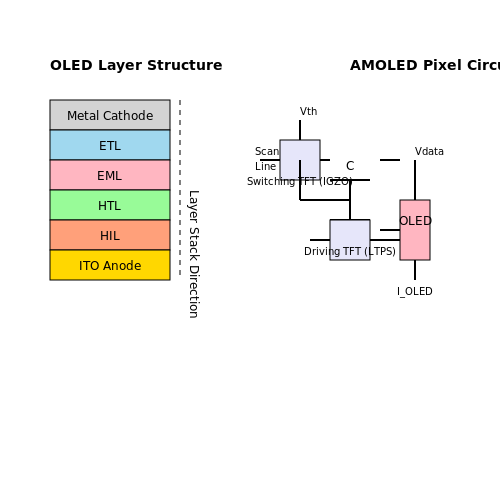
The emissive nature of OLEDs enables simpler display architectures compared to LCDs, eliminating the need for backlight units. A typical RGB OLED pixel consists of:
- Anode (transparent ITO)
- Hole injection layer (HIL)
- Hole transport layer (HTL)
- Emissive layer (EML)
- Electron transport layer (ETL)
- Cathode (low work function metal)
The charge balance factor γ critically determines efficiency:
where Jh and Je represent hole and electron current densities respectively. Optimal performance occurs at γ ≈ 0.5.
Active Matrix vs Passive Matrix Addressing
Modern OLED displays universally employ active matrix (AMOLED) designs with thin-film transistor (TFT) backplanes:
- Low-temperature polysilicon (LTPS): Offers high electron mobility (>100 cm²/V·s) enabling high refresh rates
- Oxide TFTs (IGZO): Provide better uniformity for large panels with lower leakage currents
The pixel circuit must compensate for threshold voltage (Vth) shifts in the driving TFT:
Color Patterning Techniques
Three dominant manufacturing approaches exist for full-color displays:
| Method | Advantages | Limitations |
|---|---|---|
| Fine Metal Mask (FMM) | High color purity | Limited resolution (~500 PPI) |
| White OLED + CF | No patterning constraints | Lower efficiency |
| Quantum Dot Color Conversion | Wide color gamut | Additional encapsulation needed |
Lifetime Considerations
The operational lifetime L0 follows Arrhenius-type degradation:
where Ea is the activation energy (typically 0.3-0.5 eV for organic materials). Blue emitters show the shortest lifetimes due to higher energy excitons.
Flexible Display Technologies
Polyimide substrates enable bendable displays with radii below 3mm. Critical parameters include:
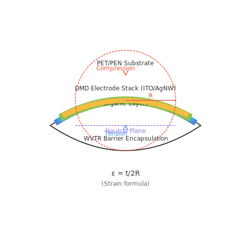
- Neutral plane engineering to minimize strain
- Thin-film encapsulation (<100nm) with WVTR < 10-6 g/m2/day
- Strain-resistant transparent electrodes (Ag nanowire networks)
5.2 Lighting: Flexible and Transparent Panels
Mechanisms of Flexibility in OLED Lighting
The mechanical flexibility of OLED panels arises from the use of organic semiconductor materials deposited on plastic substrates such as polyethylene terephthalate (PET) or polyethylene naphthalate (PEN). Unlike rigid glass, these polymers enable bending radii as small as 1–5 mm without fracture. The critical parameters governing flexibility include:
where ε is the strain, t is the substrate thickness, and R is the bending radius. For PET (typically 50–200 μm thick), maintaining ε < 1.5% ensures operational stability.
Transparent Electrode Architectures
Transparent OLEDs (TOLEDs) require electrodes with high optical transparency (>80%) and low sheet resistance (<50 Ω/sq). Common solutions include:
- Indium Tin Oxide (ITO): Industry standard but brittle; alternatives like silver nanowires or graphene are preferred for flexible designs.
- Conductive Polymers: PEDOT:PSS offers mechanical compliance but suffers from higher resistivity.
- Dielectric/Metal/Dielectric (DMD): Thin metal layers (e.g., Ag) sandwiched between high-refractive-index dielectrics (e.g., MoO3/Ag/MoO3) achieve 85% transparency at 15 Ω/sq.
Encapsulation Challenges
Flexible OLEDs demand robust encapsulation to prevent moisture/oxygen ingress, which degrades organic layers. Multilayer barriers combining:
- Inorganic Layers (Al2O3, SiNx): Provide low water vapor transmission rates (WVTR < 10−6 g/m2/day).
- Organic Buffers: Polyacrylate layers relieve mechanical stress during bending.
Performance Trade-offs
Flexible OLEDs exhibit reduced efficiency compared to rigid counterparts due to:
where ΔR/R0 quantifies resistance increase from electrode microcracking. State-of-the-art flexible panels achieve 60–80 lm/W versus 90–110 lm/W for glass-based OLEDs.
Applications and Case Studies
Notable implementations include:
- Automotive Lighting: BMW’s 2021 concept car featured curved OLED taillights with 0.5 mm thickness.
- Architectural Integration: LG’s 55-inch transparent OLED windows maintain 40% transparency while emitting 300 cd/m2 luminance.
Future Directions
Research focuses on stretchable OLEDs using elastomeric substrates and serpentine interconnects, with prototypes achieving 30% strain tolerance. Hybrid perovskite-OLED structures are also emerging for enhanced color purity.
5.3 Emerging Applications: Biomedical and Automotive
Biomedical Applications
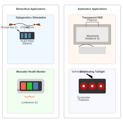
Organic Light Emitting Diodes (OLEDs) have gained significant traction in biomedical applications due to their flexibility, biocompatibility, and tunable emission spectra. One prominent use is in wearable health monitors, where OLEDs serve as photoplethysmography (PPG) sensors for real-time heart rate and oxygen saturation monitoring. The thin-film nature of OLEDs allows seamless integration into skin-adherent patches, enabling continuous physiological tracking without discomfort.
Another breakthrough is in optogenetics, where OLED arrays stimulate genetically modified neurons with precise wavelengths. Unlike traditional light sources, OLEDs offer localized stimulation with minimal heat generation, reducing tissue damage. The emission spectrum can be tailored to match the activation wavelength of opsins, typically around 470 nm (blue) or 560 nm (green). The irradiance I required for neuronal activation follows:
where P is optical power, A is illumination area, ϕ is photon flux, and h·u is photon energy.
OLEDs are also being explored for in-vivo imaging and drug delivery systems. For instance, OLED-based endoscopes provide high-resolution imaging with lower power consumption than conventional LED light sources. In drug delivery, OLEDs trigger photochemical reactions in light-sensitive hydrogels, enabling controlled release of therapeutics.
Automotive Applications
In the automotive sector, OLEDs are revolutionizing lighting and display systems. Their ultra-thin form factor and high contrast ratios make them ideal for transparent head-up displays (HUDs), projecting critical driving information onto windshields without obstructing the view. The luminance L required for daylight visibility is derived from:
where Ev is ambient illuminance, R is reflectance, and T is transparency.
OLED taillights and interior lighting are becoming standard in premium vehicles due to their design flexibility and energy efficiency. Unlike LEDs, OLEDs provide homogeneous illumination without hotspots, enhancing aesthetic appeal and safety. For example, Mercedes-Benz's "Digital Light" system uses over one million micromirrors per headlight, paired with OLED elements for adaptive high-beam patterns.
Emerging research focuses on self-healing OLEDs for automotive applications, where microcapsules filled with conductive polymers repair minor scratches autonomously. This addresses durability concerns in harsh environments. The healing efficiency η is quantified as:
where Lpre and Lpost are luminance before and after damage.
Challenges and Future Directions
Despite these advancements, OLEDs face challenges in biomedical and automotive applications. In medical devices, long-term stability under physiological conditions remains a hurdle, as moisture and oxygen diffusion degrade organic layers. Encapsulation techniques using atomic layer deposition (ALD) of Al2O3 show promise, with water vapor transmission rates (WVTR) below 10−6 g/m2/day.
For automotive use, achieving high brightness (>10,000 cd/m2) while maintaining efficiency is critical. Phosphorescent OLEDs (PHOLEDs) with iridium-based emitters achieve external quantum efficiencies (EQE) up to 30%, but cost reduction through alternative materials like thermally activated delayed fluorescence (TADF) emitters is an active research area.
6. Improving Stability and Lifespan
6.1 Improving Stability and Lifespan
The operational stability and lifespan of organic light-emitting diodes (OLEDs) are critical for commercial viability, particularly in display and lighting applications. Degradation mechanisms in OLEDs arise from electrochemical, thermal, and morphological instabilities, necessitating material and device-level optimization strategies.
Material-Level Stabilization
Chemical degradation of organic emitters and charge transport layers is a primary failure mode. Key approaches include:
- Molecular engineering of emitters with rigid, sterically hindered structures to suppress aggregation-induced quenching and electrochemical decomposition.
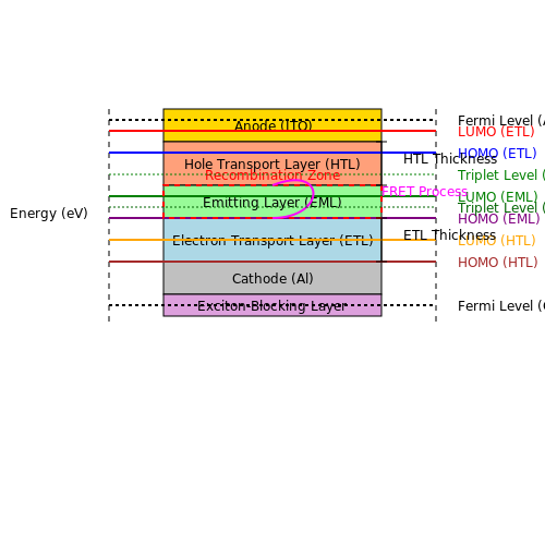
- Host-guest systems where emitters are diluted in a stable matrix, reducing exciton-exciton annihilation. The Förster resonance energy transfer (FRET) efficiency must satisfy:
where \(k_{FRET}\) is the energy transfer rate and \(k_{nr}\) the non-radiative decay rate.
- Cross-linkable materials that form thermally stable networks, preventing phase separation at operating temperatures up to 85°C.
Device Architecture Optimization
Charge balance is critical to prevent electrode degradation and non-radiative recombination at interfaces. The recombination zone can be controlled by:
- Precise tuning of electron/hole transport layer thicknesses to match carrier mobilities.
- Introduction of exciton-blocking layers (EBLs) with higher triplet energies than the emitting layer.
The optimal thickness ratio follows from the continuity equation for charge carriers:
where \(J\) is current density, \(d\) the layer thickness, \(\tau\) the carrier lifetime, and \(\beta\) the bimolecular recombination coefficient.
Encapsulation Techniques
Environmental degradation from moisture and oxygen ingress is addressed through:
- Thin-film barriers using alternating inorganic/organic layers with water vapor transmission rates (WVTR) below 10-6 g/m2/day.
- Getter materials that chemically trap permeants, with absorption capacity \(Q\) given by:
where \(\Delta P\) is pressure drop, \(V\) volume, \(R\) the gas constant, and \(T\) temperature.
Accelerated Aging Models
Lifespan prediction employs Arrhenius-type acceleration factors:
where \(t_{50}\) is time to 50% luminance decay, \(E_a\) activation energy, \(J\) current density, and \(n\) the acceleration factor (typically 1.5-2 for OLEDs).
Advanced encapsulation methods like atomic layer deposition (ALD) of Al2O3 have demonstrated operational lifetimes exceeding 100,000 hours at 100 cd/m2 initial luminance.
6.2 Reducing Manufacturing Costs
The high manufacturing costs of organic light-emitting diodes (OLEDs) have historically limited their widespread adoption compared to conventional display technologies. However, advancements in materials, deposition techniques, and substrate handling have significantly lowered production expenses. This section examines key strategies for cost reduction while maintaining performance.
Material Optimization
The selection and synthesis of organic emitters play a critical role in cost efficiency. Phosphorescent and thermally activated delayed fluorescence (TADF) materials reduce the need for rare metals like iridium, lowering material expenses. Solution-processable small molecules and polymers enable inkjet or roll-to-roll printing, eliminating costly vacuum deposition steps.
Here, ηEQE is the external quantum efficiency, γ the charge balance factor, ηPL the photoluminescence quantum yield, and ϕr the radiative exciton fraction. Optimizing these parameters allows cheaper materials to achieve performance parity with expensive alternatives.
Deposition Techniques
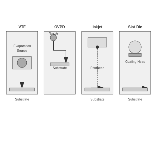
Traditional vacuum thermal evaporation (VTE) is energy-intensive and requires high-purity materials. Alternative methods include:
- Organic vapor phase deposition (OVPD): Enables precise control of film morphology at lower temperatures.
- Inkjet printing: Reduces material waste by depositing organic layers only where needed.
- Slot-die coating: Compatible with roll-to-roll processing for large-area fabrication.
Substrate and Encapsulation
Replacing rigid glass with flexible plastic substrates (e.g., polyethylene naphthalate, PEN) reduces weight and enables continuous processing. Thin-film encapsulation (TFE) using alternating layers of inorganic and organic materials provides moisture barriers at lower costs than traditional glass lids.
Manufacturing Scalability
Transitioning from batch processing to roll-to-roll (R2R) production increases throughput and reduces unit costs. Key challenges include:
- Alignment tolerances for multilayer deposition.
- Uniformity control across large areas.
- Integration of thin-film transistors (TFTs) for active-matrix backplanes.
Recent developments in laser patterning and self-aligned printing techniques have addressed many of these issues, enabling R2R production of OLED lighting panels and flexible displays.
Case Study: Cost Breakdown
A comparative analysis of 55-inch OLED TV manufacturing shows material costs decreasing from $$220/m2 in 2015 to $$85/m2 in 2023, primarily through:
- 30% reduction in emitter material costs.
- 40% savings from transition to solution processing.
- 25% lower encapsulation expenses via TFE adoption.
6.3 Next-Generation OLED Materials
Thermally Activated Delayed Fluorescence (TADF) Emitters
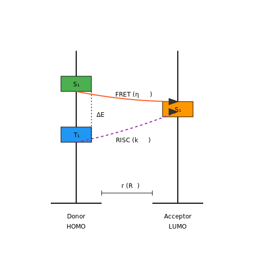
Thermally Activated Delayed Fluorescence (TADF) materials have emerged as a promising alternative to traditional phosphorescent OLEDs due to their ability to harvest both singlet and triplet excitons without relying on heavy metals. The key mechanism involves reverse intersystem crossing (RISC), where triplet excitons are upconverted to singlet states via thermal energy. The efficiency of TADF is governed by the energy gap (ΔEST) between the singlet (S1) and triplet (T1) states:
Recent advancements include donor-acceptor (D-A) molecular designs with spatially separated highest occupied molecular orbitals (HOMOs) and lowest unoccupied molecular orbitals (LUMOs) to minimize ΔEST. For instance, carbazole-based donors paired with triazine acceptors achieve ΔEST values below 0.1 eV, enabling near-unity photoluminescence quantum yields (PLQYs).
Hyperfluorescence Systems
Hyperfluorescence combines TADF emitters with fluorescent dopants to achieve narrow emission spectra and high stability. The TADF host acts as an exciton harvester, transferring energy via Förster resonance energy transfer (FRET) to the fluorescent emitter. The FRET efficiency (ηFRET) is given by:
where R0 is the Förster radius and r is the donor-acceptor distance. State-of-the-art systems using blue TADF sensitizers (e.g., DMAC-DPS) and ultrapure green emitters (e.g., DBP) achieve external quantum efficiencies (EQEs) exceeding 20% with full-width-at-half-maximum (FWHM) values under 30 nm.
Metal-Free Phosphorescent Materials
Heavy-metal-free phosphors leverage organic radicals or multi-resonance effects to enable spin-orbit coupling. For example, nitrogen-centered radicals exhibit microsecond-scale lifetimes and >90% PLQYs in rigid matrices. The radiative decay rate (kr) for such systems is enhanced by spin-vibronic coupling:
where n is the refractive index, u is the transition frequency, and μ is the transition dipole moment. Practical implementations include boron-nitrogen coordinated systems (e.g., BNCz) with EQEs rivaling iridium complexes.
Perovskite Nanocrystal Hybrids
Halide perovskite nanocrystals (PeNCs) embedded in organic matrices offer tunable emission across the visible spectrum with high color purity. The charge injection balance in PeNC-OLEDs is critical and modeled by:
where J is current density, ΔEb is the injection barrier, and μ is carrier mobility. Recent work demonstrates CsPbBr3-based hybrids with 100 cd/A efficiency and >10,000-hour operational stability at 1000 nits.
Supramolecular Assemblies
Supramolecular interactions (e.g., hydrogen bonding, π-stacking) enable precise control over molecular orientation and packing. For example, porphyrin-based assemblies exhibit polarized emission with anisotropy ratios >0.8, beneficial for augmented reality displays. The orientation parameter (κ2) in such systems is derived from transition dipole alignment:
where θD, θA are donor/acceptor angles relative to the intermolecular axis, and ϕ is the azimuthal angle difference.
7. Key Research Papers and Patents
7.1 Key Research Papers and Patents
- Organic Light‐Emitting Diodes: Pushing Toward the Limits and Beyond ... — Organic light-emitting diodes (OLEDs) are established as a mainstream light source for display applications and can now be found in a plethora of consumer electronic devices used daily. This success can be attributed to the rich luminescent properties of organic materials, but efficiency enhancement made over the last few decades has also ...
- Organic Light-Emitting Diodes (OLEDs): Materials, Photophysics, and ... — Currently, organic light-emitting diodes (OLEDs) have reached the stage of commercialization, and there have been intense efforts to use them in various applications from small- and medium-sized mobile devices to illumination equipment and large TV screens. In...
- Advancement in the technology of organic light emitting diodes — Organic light-emitting diodes (OLEDs) have been seen as one of the most promising technologies for future displays. A number of materials have been developed an ... In this paper, we will study the newer technological advancements that has improved the manufacturing process and application of organic LED's. ... Electronic ISBN: 978-1-5090-3294 ...
- Nanostructures in Organic Light‐Emitting Diodes: Principles and Recent ... — Organic light-emitting diodes (OLEDs) in recent years have emerged as a leading display technology and the popularity of OLEDs is attributed to their numerous advantages, including the ability to produce natural color, achieve a true black state, consume low consumption, exhibit fast response, and be compatible with flexible devices.
- Organic Light-Emitting Diodes (OLEDs) | SpringerLink — According to the working principle of the device, the research of organic electroluminescent materials and devices primarily includes the following several directions: active layer materials (the three primary color light-emitting materials, red, green, and blue, including fluorescent materials and phosphorescent materials), compatible materials for device fabrication (hole and electron ...
- Recent advances in organic light-emitting diodes: toward smart lighting ... — Organic light-emitting diodes (OLEDs) have rapidly grown as one of the leading technologies for full-color display panels and eco-friendly lighting sources due to their outstanding features including superior color quality, wide viewing angle, mercury-free manufacture, fascinating flexibility, etc. A variety of materials, device architectures, as well as processing techniques have been ...
- PDF Organic Light Emitting Diodes (OLED) ONLINE Final1 - Europa — An OLED (organic light-emitting diode) is a light-emitting diode (LED) in which the emissive electroluminescent layer is a film of organic compound that emits light in response to an electric current. OLEDs are used to create digital displays in devices such as television screens, computer monitors, portable systems such as mobile phones,
- Organic Light Emitting Diodes (OLED) - ResearchGate — Other types of technology applications, such as those involving organic light emitting diodes (OLEDs) and organic field-effect transistors (OFETs) as one of the most populous electroluminescent ...
- PDF Organic Light Emitting Diode (Oled) - Ajer — This work discusses the Organic Light Emitting Diode (OLED) with interest on how it works its material properties, its prospects, limitations and application areas. This work is intended to showcase the groundbreaking technological success in the electronics display world, in this masterpiece called the OLED. This research is also intended to ...
- (PDF) Organic light-emitting diodes (OLEDs) - ResearchGate — In this paper we present our results concerning the role of 2,9-Dimethyl-4,7-diphenyl-1,10-phenanthroline (bathocuproine, BCP) in OLED structures with emissive layer of Tris-(8-hydroxyquinoline ...
7.2 Industry Reports and Market Analysis
- Organic Light Emitting Diodes Market by Type, Application, End-User ... — Organic Light Emitting Diodes Market by Type (AMOLED, PMOLED), Application (OLED Display, OLED Lighting), End-User - Global Forecast 2025-2030 - The Organic Light Emitting Diodes Market was valued at USD 18.34 billion in 2023, expected to reach USD 21.19 billion in 2024, and is projected to grow at a CAGR of 15.60%, to USD 50.64 billion by 2030.
- Global Organic Light-emitting Diodes (OLEDs£©Microdisplay Market Report ... — Organic Light-emitting Diodes (OLEDs£©Microdisplay market report introduces market overview with product specification, type, application, top key players, industry growth revenue and CAGR status. Furthermore, it contains an analysis of current market dynamics, future developments, and market growth opportunities.The purpose of this report is to provide a telescopic view of the current ...
- Organic Light Emitting Diode (OLED) Global Market Report 2025 — The organic light emitting diode (oled) market global report from the Business Research Company answers all these questions and many more. The report covers market characteristics, size and growth, segmentation, regional and country breakdowns, competitive landscape, market shares, trends and strategies for this market.
- Organic Light Emitting Diode (Oled) Market Size & Overview By 2029 — Global Organic Light Emitting Diode (OLED) Market, By Product Type (Display, Lighting), Technology (PMOLED, AMOLED, Transparent OLED, Top-Emitting OLED, Foldable OLED, White OLED), End Use (Consumer Electronics, Automotive, Retail, Industrial, Commercial, Aerospace and Defense, Healthcare, Others) - Industry Trends and Forecast to 2029.
- Organic Light Emitting Diodes Market Research Report 2032 — The global Organic Light Emitting Diodes (OLED) market size was valued at approximately USD 25.4 billion in 2023 and is projected to reach around USD 85.1 billion by 2032, growing at a compound annual growth rate (CAGR) of 14.5% during the forecast period.
- Organic Light Emitting Diode (OLED) Market Share Report 2025-2034 — The Organic Light Emitting Diode (OLED) Market is projected to grow at 12.7% CAGR, reaching $$86.49 Billion by 2029. Where is the industry heading next? Get the sample report now!
- Global Organic Light Emitting Diode (OLED) Market 2025 — Organic Light Emitting Diode (OLED) Key Market Trends : Increase in OLED Adoption for Displays: The demand for OLEDs in consumer electronics like smartphones, televisions, and wearable devices is on the rise due to their superior color quality, thinner design, and energy efficiency. Growth in Automotive Applications: OLED technology is gaining traction in the automotive industry for ...
- Organic Light-Emitting Diode Market Analysis APAC, North America ... — Global Organic Light-Emitting Diode size is estimated to grow by USD 65777.8 million from 2024 to 2028 at a CAGR of 19% with the oled display having largest market share.
- Organic Light Emitting Diode (OLED) Market: Global Industry — Clear representation of competitive analysis of key players by Application, price, financial position, Product portfolio, growth strategies, and regional presence in the Global Organic Light Emitting Diode Market make the report an investor's guide. Organic Light Emitting Diode (OLED) Market Scope: Inquire before buying
- Organic Light Emitting Diode (OLED) Market Research Report 2032 — The global Organic Light Emitting Diode (OLED) market size is expected to experience a significant surge, with projections estimating it to increase from $$38 billion in 2023 to approximately $118 billion by 2032, reflecting a robust compound annual growth rate (CAGR) of 13.5% during this forecast period.
7.3 Recommended Books and Online Resources
- Handbook of Organic Materials for Optical and (Opto)Electronic Devices — 18.2 Basics of organic light-emitting diodes (OLEDs) 18.3 Pin organic light-emitting diodes (OLEDs) 18.4 Highly efficient monochrome organic light-emitting diodes (OLEDs) 18.5 Highly efficient white organic light-emitting diodes (OLEDs) 18.6 Degradation of organic light-emitting diodes (OLEDs) 18.7 Future trends; Chapter 19: Organic spintronics ...
- Organic light-emitting diodes (OLEDs) - SearchWorks catalog — Applications discussed include displays, microdisplays and transparent OLEDs, sensors and large-area OLED lighting panels. Organic light-emitting diodes (OLEDs) is a standard reference for engineers working in lighting, display technology and the consumer electronics sectors, as well as those researching OLEDs. (source: Nielsen Book Data)
- Organic Light-Emitting Diodes (OLEDs) - 1st Edition - Elsevier Shop — Part III: Applications of organic light-emitting diodes (OLEDs) in displays and solid-state lighting. Chapter 15: Active matrix, organic light-emitting diodes (AMOLEDs) for displays. Abstract: 15.1 Introduction. 15.2 OLED display business ecosystem creation. 15.3 Lifetime and burn-in effect. 15.4 Power consumption. 15.5 OLED television
-
OLED Displays and Lighting | Wiley —
Explains the fundamentals and practical applications of flat and flexible OLEDs for displays and lighting
Organic light-emitting diodes (OLEDs) have emerged as the leading technology for the new display and lighting market. OLEDs are solid-state devices composed of thin films of organic molecules that create light with the application of electricity. OLEDs can provide ...
- Solution-Processed Organic Light-Emitting Devices — Solution-Processed Organic Light-Emitting Devices provides a comprehensive reference on the principles and advances in materials design, device structures, and processing technologies of organic light-emitting diodes (OLEDs). Most importantly, the book analyses the dynamics of thin-film growth from solutions such as solvent orthogonalization, coffee-ring effects, and interfacial adhesion.
- Organic light emitters | Organic Electronics: Foundations to ... — This chapter introduces the design and fundamental concepts of organic light emitting diodes (OLEDs) and organic semiconductor lasers (OSLs). The chapter begins by describing device architectures used in fluorescent, phosphorescent, and thermally assisted delayed fluorescent (TADF) devices.
- Materials for Organic Light Emitting Devices | SpringerLink — Organic light emitting devices (OLED) are attracting much attention for light and thin flat panel display [].The typical device structure is illustrated schematically in Fig. 7.1.It has a simple multilayer structure where an organic semiconductor thin film is sandwiched with an anode and a cathode.
- Optoelectronic Polymers for Organic Light-emitting Diodes (OLEDs) — Continuing the exploration of the conductive and semiconducting properties of polymers, Friend et al. 1 at the University of Cambridge, UK, successfully fabricated the first polymer light-emitting diodes (PLEDs) in 1990 using poly(p-phenylene acetylene) (PPV) as an emissive layer (EML). Compared with small molecule OLEDs, PLEDs have unique ...
- Highly Efficient OLEDs[Book] - O'Reilly Media — Book description. The essential resource that offers a comprehensive understanding of OLED optimizations. Highly Efficient OLEDs. Materials Based on Thermally Activated Delayed Fluorescence (TADF) offers substantial information on the working principle of OLEDs and on new types of emitting materials (organic and inorganic). As the authors explain, OLEDs that use the Singlet-Harvesting ...
- Solution-Processed Organic Light-Emitting Devices - ResearchGate — Organic light emitting diodes (OLEDs) have been extensively investigated and significantly improved over the past two decades. The mechanism for electroluminescent (EL) phenomenon involves in the ...