Zinc Sulfide Electroluminescent Panels
1. Principles of Electroluminescence
1.1 Principles of Electroluminescence
Mechanism of Electroluminescence
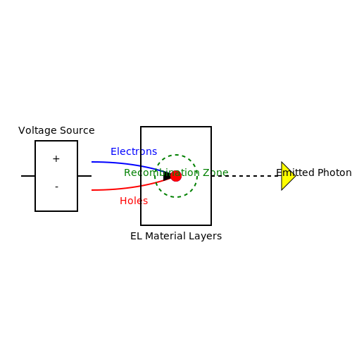
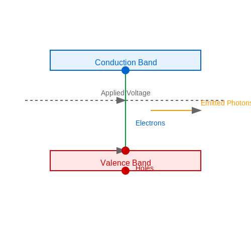
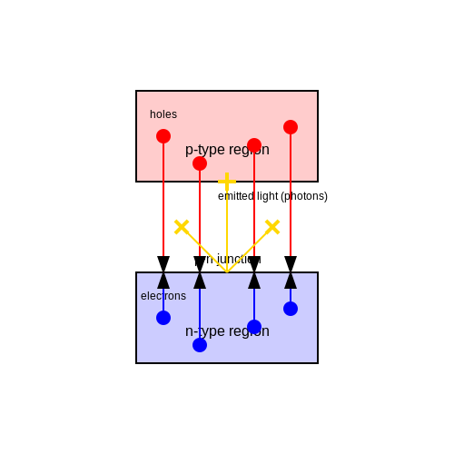
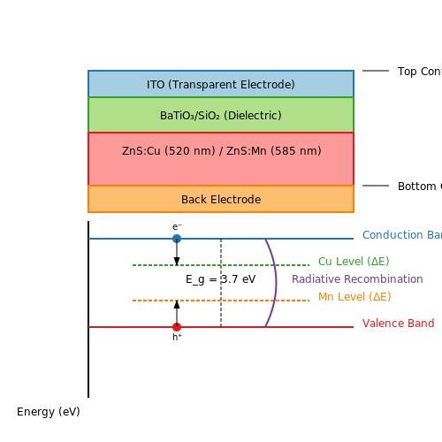
Electroluminescence (EL) is the phenomenon where a material emits light in response to an applied electric field. In zinc sulfide (ZnS) electroluminescent panels, this occurs due to the recombination of electron-hole pairs within the semiconductor lattice. When an alternating electric field is applied, electrons are accelerated into the conduction band, gaining sufficient energy to excite luminescent centers—typically dopants like copper (Cu) or manganese (Mn). These centers subsequently relax radiatively, emitting photons.
Energy Band Structure and Carrier Dynamics
ZnS is a direct bandgap semiconductor (~3.7 eV), making it suitable for efficient light emission. Under an AC field, impact ionization generates electron-hole pairs. The electric field strength E must exceed a threshold to ensure sufficient carrier acceleration:
where Eg is the bandgap energy, q is the electron charge, and λmean is the mean free path. The emitted photon wavelength λ is determined by the dopant's energy levels:
where ΔE is the energy difference between the excited and ground states of the luminescent center.
Role of Phosphor and Dopants
Undoped ZnS exhibits weak EL. Introducing activators like Cu (green emission at ~520 nm) or Mn (orange emission at ~585 nm) creates discrete energy states within the bandgap. The host lattice (ZnS) provides the matrix, while dopants serve as recombination centers. The luminance L follows:
where C is a material-dependent constant. Higher dopant concentrations increase emission intensity but can lead to quenching due to non-radiative recombination.
AC vs. DC Electroluminescence
ZnS EL panels predominantly use AC excitation (typically 50–1000 Hz, 50–300 V) due to:
- Higher efficiency: AC fields prevent electrode degradation and enable impact ionization cycling.
- Reduced aging: DC operation causes ion migration, leading to dark spot formation.
The luminance-voltage relationship in AC-driven panels is empirically modeled as:
where L0, V0, n, and β are fitting parameters derived from the phosphor's characteristics.
Quantum Efficiency and Loss Mechanisms
The internal quantum efficiency ηint is given by:
where τrad and τnonrad are radiative and non-radiative lifetimes. Dominant loss mechanisms include:
- Auger recombination: Carrier-carrier scattering dissipates energy as heat.
- Surface states: Unpassivated defects trap carriers, reducing emission.
Practical Considerations in Panel Design
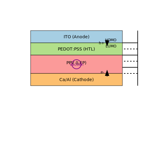
Modern ZnS EL panels use a layered structure:
- Transparent electrode: Indium tin oxide (ITO) for high conductivity and optical transparency.
- Dielectric layer: BaTiO3 or SiO2 to prevent dielectric breakdown.
- Phosphor layer: ZnS:Cu or ZnS:Mn particles embedded in a polymer matrix.
Optimal thickness balances field uniformity and light extraction. The dielectric layer's permittivity εr must satisfy:
to ensure voltage division across the phosphor layer.
Material Properties of Zinc Sulfide
Crystal Structure and Phase Transitions
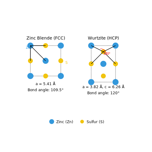
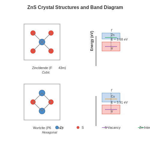
Zinc sulfide (ZnS) exhibits two primary crystalline phases: cubic zincblende (sphalerite) and hexagonal wurtzite. The zincblende structure (space group F$$\overline{4}$$3m) consists of a face-centered cubic lattice with Zn2+ and S2− ions occupying alternating tetrahedral sites. The wurtzite phase (space group P63mc) features a hexagonal close-packed arrangement with a c/a ratio of ~1.64. Phase transitions occur at ~1020°C (zincblende to wurtzite) and ~1290°C (decomposition).
Electronic Band Structure
ZnS is a direct bandgap semiconductor with the conduction band minimum and valence band maximum both at the Γ-point. The spin-orbit coupling splits the valence band into three subbands:
The effective masses are anisotropic, with me* ≈ 0.28m0 for electrons and mhh* ≈ 1.76m0 for heavy holes.
Optical Properties
The refractive index n follows the Sellmeier dispersion relation in the transparent region (400–1200 nm):
Photoluminescence spectra show characteristic blue (468 nm) and green (530 nm) emission bands due to sulfur vacancies (VS) and zinc interstitials (Zni). The radiative recombination lifetime τr ranges from 10−6 to 10−3 s depending on doping.
Electrical Characteristics
Undoped ZnS exhibits high resistivity (>106 Ω·cm) due to self-compensation. Copper doping (0.01–0.1 wt%) creates acceptor levels 0.9 eV above the valence band, enabling electroluminescence. The field-dependent conductivity follows Poole-Frenkel emission:
where φB ≈ 0.7 eV is the trap barrier height and ε = 8.3ε0 the permittivity.
Thermal and Mechanical Properties
- Thermal conductivity: 27 W/m·K (300 K)
- Thermal expansion coefficient: 6.5×10⁻⁶ K−1
- Vickers hardness: 2.5 GPa (zincblende), 3.2 GPa (wurtzite)
- Young's modulus: 75 GPa
The Debye temperature θD = 315 K influences phonon scattering rates critical for high-field electroluminescent operation.
Defect Chemistry
Native defects dominate material behavior:
| Defect | Formation Energy (eV) | Role in EL |
|---|---|---|
| VS | 1.2 | Green emission centers |
| Zni | 0.8 | Donor states |
| CuZn | 0.3 | Blue emission activators |
Mn2+ doping (0.5–2 mol%) introduces orange emission at 585 nm via 4T1→6A1 transitions with quantum efficiency >60%.
1.3 Band Gap and Emission Characteristics
Fundamentals of Band Gap in ZnS
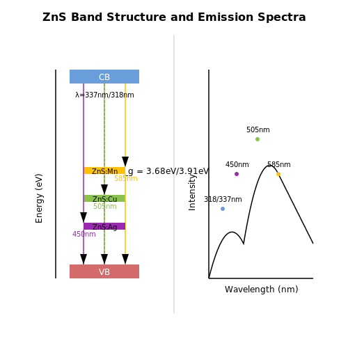
The electroluminescent properties of zinc sulfide (ZnS) are governed by its band structure, particularly the energy difference between the valence band (VB) and conduction band (CB). ZnS is a direct band gap semiconductor with a room-temperature band gap Eg of approximately 3.68 eV for the cubic zincblende phase and 3.91 eV for the hexagonal wurtzite phase. The band gap energy determines the minimum photon energy emitted during electron-hole recombination, following the relation:
where h is Planck's constant, ν is the photon frequency, c is the speed of light, and λ is the emission wavelength. For pure ZnS, this corresponds to an ultraviolet emission at ~337 nm (zincblende) or ~318 nm (wurtzite).
Doping and Emission Spectrum Control
Pure ZnS emits in the UV range, but practical electroluminescent devices require visible light emission. This is achieved through transition metal or rare-earth doping, which introduces intra-bandgap states that facilitate radiative recombination at lower energies. The most common dopants and their emission characteristics are:
- Cu (Copper): Creates green emission (~505 nm) through donor-acceptor pair transitions involving sulfur vacancies.
- Mn (Manganese): Produces yellow-orange emission (~585 nm) via 4T1→6A1 transitions of Mn2+ ions.
- Ag (Silver): Generates blue emission (~450 nm) through shallow trap states.
The emission wavelength λem can be approximated for a given dopant by:
where Et represents the trap energy level introduced by the dopant.
Electric Field Dependence
The electroluminescent intensity I in ZnS follows an exponential relationship with the applied electric field F:
where F0 is a characteristic field strength parameter dependent on the phosphor composition and device structure. This nonlinear behavior arises from impact ionization processes that accelerate electrons to energies sufficient for impact excitation of luminescent centers.
Temperature Effects on Emission
The temperature dependence of ZnS electroluminescence reveals competing effects:
- Thermal quenching: Above ~150°C, non-radiative recombination increases, reducing quantum efficiency.
- Thermal activation: Below room temperature, carrier mobility increases, enhancing impact excitation probability.
The temperature-dependent intensity I(T) can be modeled by:
where Ea is the activation energy for thermal quenching, k is Boltzmann's constant, and C is a material constant.
2. Panel Architecture and Layer Composition
Panel Architecture and Layer Composition
Zinc sulfide (ZnS) electroluminescent (EL) panels operate based on a multilayer thin-film structure optimized for efficient photon emission under an alternating electric field. The architecture consists of several critical layers, each serving a distinct electroluminescent, conductive, or insulating function.
Core Layer Structure
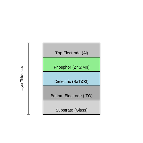
The standard ZnS EL panel is composed of the following layers, listed from bottom to top:
- Substrate: Typically glass or flexible polymer (e.g., PET), providing mechanical support.
- Bottom electrode: A transparent conductive layer, usually indium tin oxide (ITO), serving as the anode.
- Dielectric layer: High-permittivity material (e.g., BaTiO3 or Ta2O5) to enhance field strength across the phosphor.
- Phosphor layer: ZnS doped with luminescent centers (e.g., Cu for green emission, Mn for orange).
- Top electrode: Often a reflective metal (e.g., aluminum) or another transparent conductor.
Phosphor Layer Physics
The ZnS:Mn/Cu phosphor layer is the active luminescent component. When subjected to an AC field (typically 50–400 V at 50–1000 Hz), impact ionization excites dopant atoms, which then decay radiatively. The emitted wavelength λ depends on the dopant's energy levels:
where Eg is ZnS's bandgap (3.68 eV) and Ed is the dopant's trap depth (e.g., 2.1 eV for Cu).
Field Distribution Modeling
The electric field E across the phosphor layer is determined by the dielectric constant mismatch between layers. For a two-layer system (dielectric + phosphor):
where d denotes thickness, ϵ permittivity, and subscripts ph and di refer to the phosphor and dielectric layers, respectively.
Advanced Architectures
High-efficiency panels employ:
- Graded doping: Varying dopant concentration to optimize field uniformity.
- Distributed Bragg reflectors (DBRs): Dielectric mirrors to enhance light extraction.
- Multilayer phosphors: Stacked ZnS:Cu/ZnS:Mn for white emission via color mixing.
Fabrication Considerations
Layer uniformity is critical; variations exceeding 5% in thickness or composition cause visible luminance gradients. Industrial processes use:
- Sputtering: For ITO and dielectric layers (±3 nm uniformity).
- Screen printing: For thick-film phosphor deposition.
- Atomic layer deposition (ALD): For nanoscale dopant control in high-end panels.
The interplay between layer thickness and permittivity directly governs the panel's threshold voltage and power efficiency, as modeled by:
2.2 Deposition Techniques for Zinc Sulfide
Physical Vapor Deposition (PVD)
Physical Vapor Deposition (PVD) is a vacuum-based process where ZnS is vaporized from a solid source and deposited onto a substrate. The two primary PVD methods for ZnS are thermal evaporation and sputtering. Thermal evaporation involves heating ZnS in a crucible until it sublimates, while sputtering uses plasma to eject ZnS atoms from a target. The deposition rate R in thermal evaporation can be modeled using the Hertz-Knudsen equation:
where α is the sticking coefficient, P is the vapor pressure, m is the molecular mass, kB is the Boltzmann constant, and T is the temperature. PVD produces high-purity films with minimal contamination, making it ideal for electroluminescent applications requiring precise stoichiometry.
Chemical Vapor Deposition (CVD)
Chemical Vapor Deposition (CVD) involves reacting gaseous precursors to form a ZnS film on a heated substrate. Common precursors include zinc dialkyldithiocarbamates or zinc sulfide hydride. The reaction kinetics are governed by the Arrhenius equation:
where k is the rate constant, A is the pre-exponential factor, Ea is the activation energy, and R is the gas constant. CVD enables conformal coatings on complex geometries and allows doping during deposition by introducing additional gases like Mn for luminance enhancement.
Atomic Layer Deposition (ALD)
Atomic Layer Deposition (ALD) offers monolayer control through sequential, self-limiting surface reactions. A typical ZnS ALD cycle alternates between zinc-containing (e.g., diethylzinc) and sulfur-containing (e.g., hydrogen sulfide) precursors. The growth per cycle (GPC) is:
where Δd is the thickness change and N is the number of cycles. ALD achieves unparalleled uniformity and thickness control, critical for multilayer electroluminescent structures.
Electrodeposition
Electrodeposition grows ZnS films from an aqueous or non-aqueous electrolyte containing Zn2+ and S2− ions. The current density i follows Butler-Volmer kinetics:
where i0 is the exchange current density, α is the charge transfer coefficient, n is the number of electrons, F is Faraday’s constant, and η is the overpotential. This low-cost technique is suitable for large-area panels but requires post-deposition annealing to improve crystallinity.
Comparative Analysis
The choice of deposition method depends on application requirements:
- PVD: High purity, moderate cost, limited to line-of-sight deposition.
- CVD: Conformal coatings, scalable, but requires high temperatures.
- ALD: Atomic-level precision, low defect density, but slow deposition rates.
- Electrodeposition: Cost-effective for large areas, but lower film quality.
2.3 Electrode Materials and Configurations
Electrode Material Requirements
The performance of zinc sulfide (ZnS) electroluminescent (EL) panels is critically dependent on the choice of electrode materials. Key requirements include:
- High electrical conductivity to minimize resistive losses and ensure uniform electric field distribution.
- Optical transparency for the front electrode to allow light emission without significant attenuation.
- Chemical stability to prevent degradation under high electric fields and environmental exposure.
- Mechanical flexibility if used in bendable or wearable applications.
Common Electrode Materials
Front (Transparent) Electrodes
Indium tin oxide (ITO) is the most widely used transparent conductive oxide (TCO) due to its high transparency (>85%) and low sheet resistance (10–100 Ω/sq). Alternatives include:
- Fluorine-doped tin oxide (FTO): Lower cost but slightly higher resistivity.
- Conductive polymers (e.g., PEDOT:PSS): Flexible but prone to moisture degradation.
- Silver nanowire networks: High flexibility and conductivity, but scattering can reduce optical clarity.
Rear (Reflective) Electrodes
Aluminum is the standard rear electrode due to its high reflectivity (>90%) and low work function (4.1 eV), which enhances electron injection. Other options include:
- Silver: Higher reflectivity but more expensive.
- Graphite: Used in flexible panels, though with higher resistivity.
Electrode Configurations
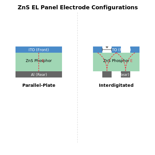
The electric field distribution in ZnS EL panels is governed by the electrode geometry. Two primary configurations are employed:
Parallel-Plate Configuration
The simplest design, where the ZnS phosphor layer is sandwiched between two planar electrodes. The luminance L is proportional to the applied field E:
where V is the applied voltage and d is the phosphor layer thickness. This configuration suffers from edge effects, causing non-uniform emission near the electrode boundaries.
Interdigitated Electrodes
Used in thick-film EL panels to enhance field uniformity. The electric field between adjacent finger electrodes follows:
where w is the finger spacing and x is the lateral position. This design reduces edge effects but requires precise patterning.
Advanced Electrode Designs
Recent research focuses on nanostructured electrodes to improve performance:
- Graded-index TCOs: Reduce interfacial reflections by gradually varying the refractive index.
- Hybrid electrodes: Combine ITO with metal grids to balance conductivity and transparency.
- Textured rear electrodes: Enhance light extraction via scattering.
Practical Considerations
Electrode selection must account for:
- Drive frequency: High-frequency AC (200 Hz–2 kHz) can cause capacitive losses in resistive electrodes.
- Adhesion layers: Thin chromium or titanium layers are often used under aluminum to prevent delamination.
- Manufacturing constraints: Sputtering for ITO vs. screen printing for conductive pastes.
Case Study: Flexible EL Panels
In wearable displays, polyethylene terephthalate (PET) substrates with ITO/PEDOT:PSS bilayer electrodes achieve sheet resistances below 50 Ω/sq while maintaining >80% transparency and bending radii under 5 mm.
3. AC vs. DC Excitation Methods
3.1 AC vs. DC Excitation Methods
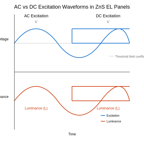
Zinc sulfide (ZnS) electroluminescent (EL) panels operate under either alternating current (AC) or direct current (DC) excitation, each with distinct physical mechanisms and performance trade-offs. The choice between AC and DC excitation affects luminance efficiency, operational lifetime, and driving circuit complexity.
AC Excitation Mechanism
AC-driven ZnS EL panels rely on impact ionization and radiative recombination within the phosphor layer. When an alternating electric field is applied, electrons are accelerated across the ZnS lattice, colliding with luminescent centers (typically Cu or Mn dopants). The resulting energy transfer produces visible light. The luminance L of an AC EL panel follows:
where L0 is a material-dependent constant, B is the threshold field coefficient, and Vrms is the root-mean-square voltage. AC excitation typically requires high-frequency (50 Hz–5 kHz) and high-voltage (50–300 Vrms) signals, necessitating an inverter circuit.
DC Excitation Mechanism
DC-driven ZnS EL panels operate via direct carrier injection at electrode interfaces. Electrons and holes recombine radiatively within the phosphor layer without requiring impact ionization. The luminance-current relationship is linear at low currents but saturates at higher densities due to non-radiative recombination:
where η is quantum efficiency, J is current density, and q is electron charge. DC panels typically operate at lower voltages (3–24 V) but suffer from faster degradation due to electrochemical reactions at the electrodes.
Comparative Analysis
- Efficiency: AC panels achieve higher lumens/watt (up to 15 lm/W) due to reduced joule heating. DC panels rarely exceed 5 lm/W.
- Lifetime: AC excitation minimizes electrode degradation, enabling 10,000+ hours at 100 cd/m². DC panels degrade rapidly beyond 2,000 hours.
- Circuit Complexity: DC panels integrate easily with battery-powered systems, while AC panels require inverters or resonant drivers.
Practical Considerations
AC excitation dominates in backlighting and large-area displays (e.g., aircraft instrumentation), whereas DC variants are restricted to low-cost, short-life applications like novelty lighting. Recent advances in pulsed DC excitation attempt to hybridize benefits, using brief high-voltage pulses (1–10 µs) to mimic AC behavior while retaining DC compatibility.
3.2 Voltage and Frequency Dependence
Electroluminescent Brightness as a Function of Voltage
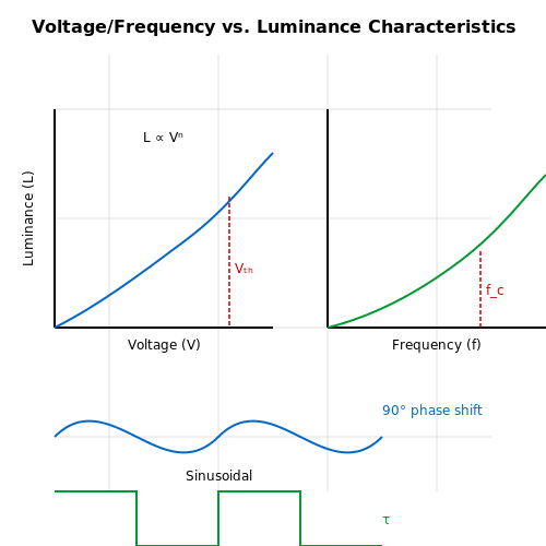
The luminance L of a zinc sulfide (ZnS) electroluminescent (EL) panel follows a power-law dependence on the applied voltage V:
where n typically ranges between 2.5 and 3.5, depending on the phosphor doping and dielectric properties. This nonlinear relationship arises from impact ionization and field-dependent carrier injection into the ZnS lattice. Empirical studies show that luminance saturates at high voltages (V > Vth) due to trap-state filling and thermal quenching.
Frequency Dependence and Time-Resolved Behavior
At a fixed voltage, luminance increases with driving frequency f up to a critical frequency fc, beyond which radiative recombination efficiency drops. The frequency response is modeled as:
where L0 is the low-frequency luminance limit. The critical frequency fc is tied to the phosphor's decay time constant τ (fc ≈ 1/(2πτ)). For ZnS:Cu,Cl, τ ranges from 1–10 µs, placing fc in the 10–100 kHz range.
Phase and Waveform Effects
EL panels exhibit higher efficiency under AC excitation due to reduced charge trapping. Symmetric waveforms (e.g., sinusoidal or square waves) yield optimal performance, while DC or asymmetric waveforms cause rapid degradation. The phase difference between current and voltage affects power dissipation:
where T is the waveform period. Capacitive reactance dominates the panel's impedance, leading to a phase shift near 90° at high frequencies.
Practical Design Implications
- Voltage Trade-offs: Higher voltages increase brightness but accelerate phosphor aging. Typical operating ranges are 50–400 Vrms.
- Frequency Optimization: Most commercial panels operate at 400–2000 Hz, balancing brightness and driver complexity.
- Waveform Selection: Inverter designs often use modified square waves to minimize harmonics while maintaining efficiency.
Mathematical Derivation of Luminance-Power Relationship
Starting from the radiative recombination rate R and assuming Shockley-Read-Hall statistics:
where B is the recombination coefficient, and n, p are carrier densities. Under high-field conditions, the injected carrier density scales as:
Combining these yields the empirical power-law form L ∝ Vn, with n reflecting the field-dependent injection efficiency.
3.3 Efficiency and Brightness Optimization
Fundamental Efficiency Considerations
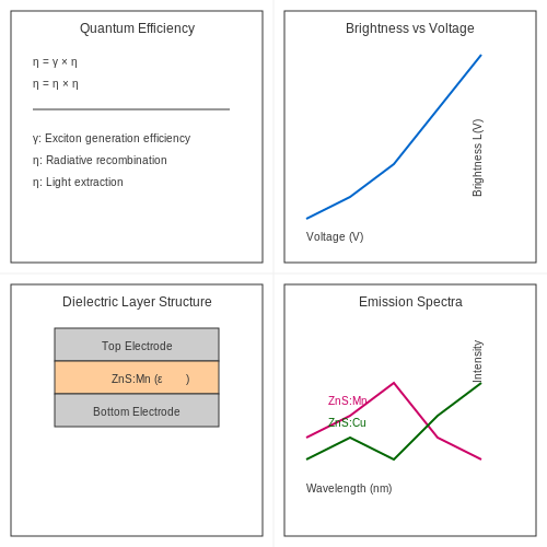
The electroluminescent (EL) efficiency of ZnS-based panels is governed by the interplay between quantum efficiency and power conversion efficiency. The internal quantum efficiency (IQE) is defined as the ratio of emitted photons to injected charge carriers:
However, not all generated photons escape the device due to total internal reflection and absorption losses. The external quantum efficiency (EQE) accounts for this:
where ηextraction is the light extraction efficiency, typically between 20-50% for standard ZnS:Mn panels.
Key Parameters Affecting Brightness
The luminance (L) of an EL panel follows the empirical relation:
where:
- L0 is the maximum achievable luminance
- Ea is the activation energy for electroluminescence
- k is Boltzmann's constant
- T is absolute temperature
- f(V) is a voltage-dependent term
The voltage dependence typically follows a power law:
where Vth is the threshold voltage, V0 is a scaling factor, and γ ≈ 2-3 for ZnS:Mn.
Optimization Strategies
1. Phosphor Layer Composition
The choice of dopant significantly impacts efficiency. For ZnS:
- Mn-doped (ZnS:Mn): Offers yellow-orange emission (585 nm) with typical efficiencies of 5-10 lm/W
- Cu-doped (ZnS:Cu): Provides green emission (520 nm) but with lower efficiency (2-5 lm/W)
- Double doping (ZnS:Mn,Ce): Can enhance efficiency through energy transfer mechanisms
2. Dielectric Layer Optimization
The dielectric constant (ε) and thickness (d) of the insulating layer critically affect field distribution:
High-κ dielectrics (e.g., BaTiO3 with ε ≈ 1000) can significantly improve field coupling to the phosphor layer compared to standard SiO2 (ε ≈ 3.9).
3. Driving Conditions
Optimal brightness occurs at:
- Frequency: 400-1000 Hz for ZnS:Mn (avoids saturation effects)
- Waveform: Bipolar pulses (reduces space charge accumulation)
- Duty cycle: 10-30% (balances brightness and lifetime)
Advanced Enhancement Techniques
Surface Plasmon Coupling
Incorporating metallic nanoparticles (e.g., Ag, Au) near the phosphor layer can enhance emission through localized surface plasmon resonance (LSPR). The enhancement factor (EF) is given by:
where Eloc is the localized field and E0 is the incident field. Practical implementations have shown 2-3× brightness improvement in ZnS:Cu systems.
Photonic Crystal Structures
Periodic nanostructures can be engineered to:
- Suppress waveguide modes (increasing ηextraction)
- Provide directional emission control
- Enhance specific wavelengths through bandgap engineering
The optimal lattice constant (a) for a square lattice is approximately:
where neff is the effective refractive index of the waveguide mode.
Thermal Management
At high drive conditions (>200 V, >1 kHz), Joule heating becomes significant. The temperature rise (ΔT) can be estimated as:
where Cphos is the phosphor capacitance, tanδ is the loss tangent, h is the heat transfer coefficient, and A is the active area. Active cooling or thermally conductive substrates (e.g., AlN) may be required for high-brightness applications.
4. Display and Backlighting Applications
4.1 Display and Backlighting Applications
Electroluminescent Mechanism in ZnS
Zinc sulfide (ZnS) electroluminescent (EL) panels operate on the principle of radiative recombination of electron-hole pairs in a high-field alternating current (AC) environment. When an AC voltage is applied across the phosphor layer, impact ionization excites dopant atoms (typically Cu or Mn), which then decay radiatively. The emitted photon energy Eph corresponds to the bandgap of ZnS (≈3.68 eV for cubic phase) modified by dopant energy levels:
where Ed is the dopant energy level, e the electron charge, ϵ the permittivity, and r the electron-hole separation distance.
Panel Architecture for Displays
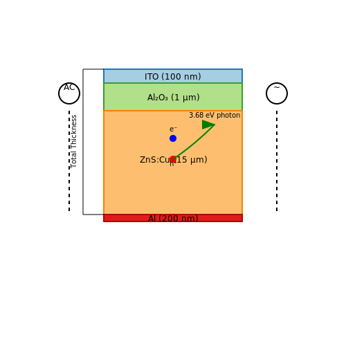
Modern ZnS EL displays employ a thin-film structure consisting of:
- Front electrode: Transparent conductive oxide (TCO) layer (typically ITO) with sheet resistance <100 Ω/sq
- Dielectric layer: High-κ material (Al2O3 or BaTiO3) with thickness 0.5–2 μm
- Phosphor layer: ZnS:Cu or ZnS:Mn particles (5–20 μm diameter) in polymer matrix
- Back electrode: Reflective aluminum or silver layer
Driving Circuit Requirements
EL panels require high-frequency (200–2000 Hz) AC excitation with voltages typically between 100–300 Vrms. The power dissipation per unit area P follows:
where C is the panel capacitance (≈1–10 nF/cm2), V the applied voltage, f the frequency, and tanδ the dielectric loss tangent. Modern drivers use resonant inverter topologies to achieve >85% efficiency.
Backlighting Design Considerations
When used as backlights for LCDs or keypads, ZnS EL panels must meet specific optical requirements:
- Luminance: 50–200 cd/m2 for most applications
- Uniformity: <15% deviation across active area
- Color temperature: 5000–6500 K for white light (achieved through blue-emitting ZnS:Cu with yellow phosphor coating)
Advantages Over Alternative Technologies
Compared to LED backlights, ZnS EL offers:
- Perfectly diffuse emission with viewing angles >170°
- No hot spots or glare effects
- Thinner profile (<0.5 mm achievable)
- Lower power consumption at moderate brightness levels
Current Research Directions
Recent advancements focus on:
- Flexible EL panels using graphene electrodes (sheet resistance down to 30 Ω/sq)
- Quantum dot-enhanced ZnS for wider color gamut (NTSC >110%)
- Integrated photovoltaic layers for self-powered displays
4.3 Comparison with Other Light-Emitting Technologies
Zinc sulfide (ZnS) electroluminescent (EL) panels exhibit distinct advantages and limitations when compared to alternative light-emitting technologies such as light-emitting diodes (LEDs), organic light-emitting diodes (OLEDs), and field-emission displays (FEDs). The primary differentiating factors include efficiency, luminance, operational lifetime, and spectral characteristics.
Luminance and Efficiency
ZnS EL panels typically achieve luminance levels between 50 and 200 cd/m², significantly lower than inorganic LEDs (10,000–100,000 cd/m²) but comparable to OLEDs (100–1,000 cd/m²). The luminous efficiency of ZnS EL devices ranges from 5–15 lm/W, whereas modern LEDs exceed 150 lm/W. The efficiency limitation arises from the intrinsic electroluminescent mechanism:
where ηexc is the excitation efficiency, ηrad the radiative recombination efficiency, and ηout the light extraction efficiency. Due to phonon scattering and non-radiative transitions in ZnS, ηrad rarely exceeds 25%.
Spectral Characteristics
ZnS EL panels emit broad-spectrum light peaking at 450–550 nm (blue-green) or 580–620 nm (yellow-orange), depending on dopants (e.g., Cu for green, Mn for yellow). This contrasts with LEDs, which exhibit narrow emission spectra (FWHM ≈ 20–50 nm). While OLEDs also offer broad spectra, their color gamut is superior due to tailored organic molecules.
Operational Lifetime and Degradation
ZnS EL devices degrade primarily via sulfur vacancy migration under high electric fields (1–5 MV/m), leading to a luminance half-life of 5,000–10,000 hours. In contrast, LEDs surpass 50,000 hours, and OLEDs degrade due to organic material oxidation. The lifetime L of an EL panel follows:
where L0 is initial luminance, E the electric field, and α a material-dependent degradation coefficient.
Flexibility and Form Factor
Unlike rigid LED arrays, ZnS EL panels are inherently flexible, enabling conformal applications where OLEDs would suffer from moisture sensitivity. The absence of liquid components (unlike LCDs) and low thickness (< 0.5 mm) make them ideal for wearable electronics and curved displays.
Power Consumption and Drive Electronics
EL panels require AC excitation (50–400 Hz, 50–200 V), complicating driver design compared to low-voltage DC LEDs. However, their capacitive nature (1–10 nF/cm²) minimizes resistive losses:
where C is capacitance, V voltage, and f frequency. This contrasts with LEDs' P = IV dependence, where junction heating dominates efficiency losses.
Cost and Manufacturing
ZnS EL manufacturing via screen printing or physical vapor deposition is cost-effective for large areas, with material costs below $$5/m². LEDs require expensive epitaxial growth (e.g., MOCVD), while OLEDs need precision vacuum deposition, raising their costs to > $$100/m² for comparable sizes.
5. Key Research Papers and Patents
5.1 Key Research Papers and Patents
- Development and advancement of undoped and doped zinc sulfide for ... — Here, we discussed the photoluminescence, and electroluminescence, behavior of zinc sulfide and doped zinc sulfide for display applications. The report is focused on different dopant ions such as (Mn 2+ , Cu 2+ , Ni 2+ , Eu 2+ , Eu 3+ , Tb 2+ , Ce 3+ , Sm 2+ ), core/shell quantum dots, and heterostructures for white light emission.
- Optical and Excitonic Properties of Crystalline ZnS Nanowires - Springer — It is known that metal ion doping of ZnS is one of the hottest research topics, e.g., manganese (Mn) doping yields an orange-red color at ∼590 nm and copper (Cu)-doped ZnS is used in electroluminescent (EL) panels [100, 101]. Therefore, this idea can be adopted in the 1-D ZnS NWs.
- Luminescence in Sulfides: A Rich History and a Bright Future — In this Review, we discuss the rich and longstanding history of sulfide phosphor materials, dating back from at least the 17th century. Progress in the understanding of the basic principles of luminescence culminated in several typical applications, uniquely based on sulfides, such as ZnS-based powder electroluminescence and thin film electroluminescence.
- Recent progress of molecular organic electroluminescent materials and ... — Organic electroluminescence (EL) is the electrically driven emission of light from non-crystalline organic materials, which was first observed and extensively studied in the 1960s [1], [2].In 1987, a team in Kodak introduced a double layer organic light-emitting device (OLED), which combined modern thin film deposition techniques with suitable materials and structure to give moderately low ...
- Comparative study on photo and electroluminescence properties of Cu ... — The fabricated display panel using lab-made ZnS:Cu(1%) sample exhibit bright blue colour electroluminescence. ... Despite advancements in phosphor preparation techniques and development of various non-sulfide based electroluminescent materials, transition metal doped chalcogenides (e.g., ZnS, CdS, and ZnSe) have been widely explored for ...
- Smart mechanoluminescent phosphors: A review of zinc sulfide‐based ... — Abstract The quest for mechanoluminescence (ML) in zinc sulfide (ZnS) spans more than a century, initially sparked by observations of natural minerals. ... In contrast to conventional photoluminescent and electroluminescent light sources, ZnS composite elastomers have emerged as flexible, stretchable self-powered light sources with considerable ...
- ELECTROLUMINESCENT DISPLAYS - Springer — primary phosphor of choice is high-purity zinc sulfide activated with manganese. This phosphor is highly nonlinear, with discrimination ratios approaching one million. It has a long life at high luminance and can be made sunlight read able. The panels typically operate over a voltage excursion of 400 volts, peak to peak. A voltage
- Photo‐ and Electroluminescence from Zn‐Doped InN Semiconductor ... — 1 Introduction. The development of colloidal semiconductor nanocrystals (NCs) has provided a new generation of high-efficiency luminescent materials whose emission wavelength is tunable across the visible and near infrared (IR) spectral region. [] The ability to chemically engineer their structure and incorporate them within other organic and inorganic hosts has led to their widespread ...
- PDF Nanowire-based Alternating Current Oxide Powder Electroluminescent ... — A novel type of alternating-current (AC) powder electroluminescent (EL) device that relies on nanowire-phosphor heterogeneous junction structure has been developed. It shows promise for manufacturing of highly stable powder EL devices. To pursue this goal, manganese ion (Mn2+)-doped zinc germanate (Zn 2 GeO 4:Mn) oxide phosphor was
- PDF dyuthi.cusat.ac.in — CERTIFICATE Certified that the work presented in this thesis is based on the original research done by Mr. M.K. Jayaraj, under my guidance in the Depart ment of Physics, Cochin
5.2 Recommended Books and Review Articles
- Development and advancement of undoped and doped zinc sulfide for ... — Here, we discussed the photoluminescence, and electroluminescence, behavior of zinc sulfide and doped zinc sulfide for display applications. The report is focused on different dopant ions such as (Mn 2+ , Cu 2+ , Ni 2+ , Eu 2+ , Eu 3+ , Tb 2+ , Ce 3+ , Sm 2+ ), core/shell quantum dots, and heterostructures for white light emission.
- Zinc Sulfide - an overview | ScienceDirect Topics — 3.5.2 Zinc sulfide (ZnS). Like aforementioned metals sulfides, zinc sulfide is also one of the most widely used metal sulfide material in photocatalysis, chemical industry, photoelectricity, and so on [203,204].Thus far, diverse ZnS nanostructures, such as nanoparticles, nanorods, nanodots, nanobelts, nanotubes, nanowires, and nanosheets, were generated using different innovative approaches ...
- Development and advancement of undoped and doped zinc sulfide for ... — A qualified and comprehensive study was presented in a book edited by Vij et al. [7]. ... (LEDs), flat panel displays (FPDs), electroluminescent panel, backlight, and cathode ray tube (CRT). This article focuses on a review of the doped zinc sulfide phosphor with transition metal and rare earth metals. This also includes working principle of EL ...
- A Comprehensive Review on Zinc Sulphide Thin Film by Chemical Bath ... — A Comprehensive Review on Zinc Sulphide Thin Film by Chemical Bath Deposition Techniques. ... 2. 3, 2. 4 5, 2.5 1. nm ... best crystallinity of the ZnS thin films pH is 10 and then .
- Luminescence in Sulfides: A Rich History and a Bright Future — In this Review, we discuss the rich and longstanding history of sulfide phosphor materials, dating back from at least the 17th century. Progress in the understanding of the basic principles of luminescence culminated in several typical applications, uniquely based on sulfides, such as ZnS-based powder electroluminescence and thin film electroluminescence.
- Luminescence in Sulfides: A Rich History and a Bright Future - MDPI — Sulfide-based luminescent materials have attracted a lot of attention for a wide range of photo-, cathodo- and electroluminescent applications. Upon doping with Ce3+ and Eu2+, the luminescence can be varied over the entire visible region by appropriately choosing the composition of the sulfide host. Main application areas are flat panel displays based on thin film electroluminescence, field ...
- Smart mechanoluminescent phosphors: A review of zinc sulfide‐based ... — EL, electroluminescent; EML, elastico-ML; TIEL, triboelectroluminescence; ZnS, zinc sulfide. The overall mechanism can be explained as follows: electrons excited by friction fall into shallow electron trap states and then transition to Cu impurity states, resulting in luminescence at a wavelength of 510 nm (Figure 17b ).
- Electroluminescence - 1st Edition | Elsevier Shop — The book reviews some basic observations of electroluminescence, the Gudden-Pohl and Dechene effects, the electroluminescence phenomena in zinc sulfide phosphors, in silicon carbide, and in compounds composed of elements in groups III and V of the Periodic Table (such as gallium phosphide). ... 6.1.3 Brightness and Grain Size 6.1.4 Summary of ...
- Zinc Oxide: A Fascinating Material for Photovoltaic Applications - Springer — Zinc oxide (ZnO), an attractive functional material having fascinating properties like large band gap (~3.37 eV), large exciton binding energy (~60 meV), high transparency, high thermal, mechanical and chemical stability, easy tailoring of structural, optical and electrical properties, has drawn a lot of attention for its optoelectronic applications including energy harvesting.
- Recent advances in efficient emissive materials-based OLED ... - Springer — In the present time, organic light-emitting diode (OLED) is a very promising participant over light-emitting diodes (LEDs), liquid crystal display (LCD), and also another solid-state lighting device due to its low cost, ease of fabrication, brightness, speed, wide viewing angle, low power consumption, and high contrast ratio. The most prominent layer of OLED is the emissive layer because the ...
5.3 Online Resources and Datasheets
- Development and advancement of undoped and doped zinc sulfide for ... — Here, we discussed the photoluminescence, and electroluminescence, behavior of zinc sulfide and doped zinc sulfide for display applications. The report is focused on different dopant ions such as (Mn 2+ , Cu 2+ , Ni 2+ , Eu 2+ , Eu 3+ , Tb 2+ , Ce 3+ , Sm 2+ ), core/shell quantum dots, and heterostructures for white light emission.
- Synthesis and photoluminescence properties of zinc sulfide ... — Copper-doped zinc sulfide (ZnS:Cu 2+) is also used in electroluminescent panels. It has been observed in different studies that the doping of impure Cu 2+ in the host lattice plays an important role in the luminescence process and enhances the luminescence sensitivity ( Bhargava et al., 1994 , Garlick and Gibson, 1949 , Geoffroy and Bringuiel ...
- Synthesis and photoluminescence properties of zinc sulfide ... — Copper-doped zinc sulfide (ZnS:Cu 2+) is also used in electroluminescent panels. It has been observed in different studies that the doping of impure Cu 2+ in the host lattice plays an important role in the luminescence process and enhances the luminescence sensitivity (Bhargava et al., 1994, Garlick and Gibson, 1949, Geoffroy and Bringuiel, 1992).
- Smart mechanoluminescent phosphors: A review of zinc sulfide‐based ... — EL, electroluminescent; EML, elastico-ML; TIEL, triboelectroluminescence; ZnS, zinc sulfide. The overall mechanism can be explained as follows: electrons excited by friction fall into shallow electron trap states and then transition to Cu impurity states, resulting in luminescence at a wavelength of 510 nm (Figure 17b ).
- Surface topography, structural, optical and dc electrical behaviors of ... — The prime goal of the present research is to synthesize pristine zinc sulfide (PZS) and cobalt (Co)-doped zinc sulfide (CDZS) thin films with different doping concentrations (DC) via chemical bath deposition (CBD) method. The effect of Co-doping on the surface topography, structural, optical and dc-electrical behaviors of PZS thin films has been ascertained. Scanning electron microscopy images ...
- Photonic Crystal Interactions with Electroluminescence from Zinc ... — Photonic Crystal Interactions with Electroluminescence from Zinc Sulfide Thin Films Doped with Erbium Trifluoride ... Publication Date: 2009 Language: english Physical Description: 1 online resource (113 p.) Thesis/Dissertation Information Degree: Doctorate ( Ph.D.) Degree Grantor: University of Florida ... Electronic Thesis or Dissertation ...
- PDF Electroluminescence From Zinc Sulfide Thin Films Doped With Erbium ... — electroluminescence from zinc sulfide thin films doped with erbium trifluoride by david michael devito a dissertation presented to the graduate school
- Organic Semiconductor Electroluminescent Materials — This chapter reviews the important progress made on small molecule electroluminescent materials used in organic light-emitting diode (OLED). In many cases we describe not only the material structures but also the properties associated with these materials, such as energy level, absorption and photoluminescence (PL) peaks, PL quantum yield, exciton life time, and so on.
- Effect of the Source-to-Substrate Distance on Structural ... — Zinc sulfide (ZnS) thin films with variable structural, optical, electrical, and thermoelectric properties were obtained by changing the source-to-substrate (SSD) distance in the physical-vapor-thermal-coating (PVTC) system. The films crystallized into a zinc-blende cubic structure with (111) preferred orientation.
- [PDF] ALTERNATING CURRENT THIN FILM ... - Semantic Scholar — of Dissertation Presented to the Graduate School of the University of Florida in Partial Fulfillment of the Requirements for the Degree of Doctor of Philosophy ALTERNATING CURRENT THIN FILM ELECTROLUMINESCENCE IN THE NEAR INFRARED FROM ZINC SULFIDE DOPED WITH RARE EARTHS By Ajay Kale December 2003 Chair: Dr. Paul H. Holloway Major Department: Materials Science and Engineering Near infrared ...