Power Supplies
1. Definition and Purpose of Power Supplies
Definition and Purpose of Power Supplies
A power supply is an electrical device that converts input energy from a source into a stable, regulated output suitable for powering electronic circuits. Its primary function is to provide precise voltage and current to a load while maintaining efficiency, reliability, and isolation where necessary. Power supplies are foundational in both analog and digital systems, ensuring operational integrity across applications ranging from microprocessors to high-power industrial machinery.
Fundamental Operating Principles
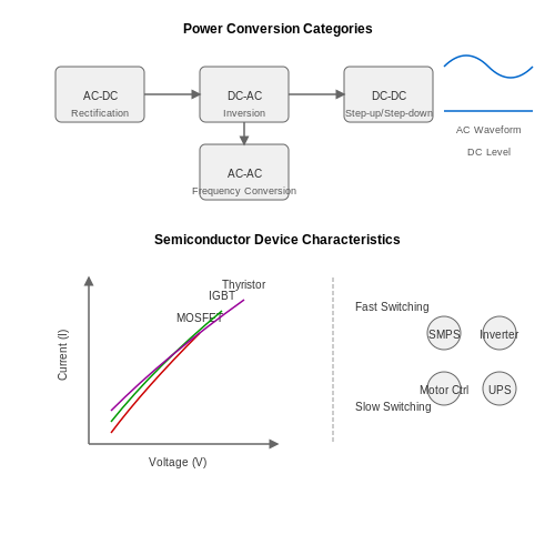
The core operation of a power supply involves energy conversion, typically from alternating current (AC) to direct current (DC), though DC-DC conversion is also common. The process can be broken down into key stages:
- Rectification: Converts AC input to pulsating DC using diodes or active switching elements.
- Filtering: Smoothes the rectified output using capacitors or inductors to reduce ripple.
- Regulation: Maintains a constant output voltage or current despite input variations or load changes, often employing feedback control loops.
For a linear power supply, the output voltage Vout is derived from a transformer-reduced AC signal:
where Vdrop is the voltage dissipated across the regulator. In contrast, switching power supplies use pulse-width modulation (PWM) to achieve higher efficiency:
Here, D represents the duty cycle of the switching signal.
Key Performance Metrics
The effectiveness of a power supply is quantified through several critical parameters:
- Line Regulation: Measures the ability to maintain output voltage despite input voltage fluctuations, expressed as a percentage:
- Load Regulation: Evaluates stability under varying load conditions.
- Efficiency: The ratio of output power to input power, crucial for thermal management and energy savings:
- Ripple and Noise: Unwanted AC components superimposed on the DC output, typically measured in millivolts peak-to-peak.
Practical Applications and Design Considerations
Power supplies are tailored to specific applications, each imposing unique constraints:
- Laboratory Power Supplies: Feature adjustable voltage/current limits and low noise for prototyping.
- Switched-Mode Power Supplies (SMPS): Dominant in consumer electronics due to compact size and high efficiency (>90%).
- Uninterruptible Power Supplies (UPS): Incorporate battery backup to mitigate power outages in critical systems.
Design challenges include electromagnetic interference (EMI) suppression, thermal dissipation, and transient response. For instance, a buck converter’s inductor must satisify:
where fsw is the switching frequency and ΔIL is the allowable current ripple.

1.2 Key Parameters: Voltage, Current, and Efficiency
Voltage Regulation and Stability
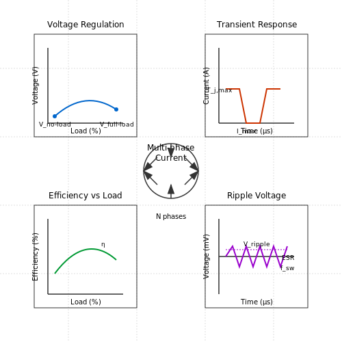
The output voltage of a power supply must remain stable under varying load conditions. Voltage regulation (Vreg) quantifies this stability and is defined as:
Where Vno-load is the unloaded output voltage and Vfull-load is the voltage at maximum rated current. High-performance power supplies achieve regulation below 1%, critical in precision instrumentation and RF applications where voltage fluctuations introduce noise or drift.
Current Delivery and Transient Response
A power supply must source sufficient current while maintaining voltage stability during load transients. The maximum current (Imax) is constrained by thermal dissipation:
Here, Tj,max is the junction temperature limit, Ta the ambient temperature, and Rth,j-a the thermal resistance. Fast transient response—often below 10 µs in modern switching supplies—requires careful control loop design to avoid oscillations during step-load changes.
Efficiency and Power Loss Mechanisms
Efficiency (η) directly impacts thermal design and energy costs, calculated as:
Losses arise from conduction (I²R), switching (e.g., MOSFET gate charge recovery), and magnetic core hysteresis. For a buck converter, conduction losses dominate at high load, while switching losses prevail at light load. Advanced topologies like resonant LLC converters achieve >95% efficiency by minimizing switching losses through zero-voltage transitions.
Case Study: Multi-phase VRM Efficiency
Voltage regulator modules (VRMs) in CPUs use interleaved phases to reduce ripple current and distribute thermal stress. For N phases, the effective RMS current per phase decreases by √N, cutting conduction losses quadratically:
This enables >90% efficiency at currents exceeding 100 A, essential for high-performance computing.
Ripple and Noise Considerations
Output ripple voltage (Vripple) in switching supplies stems from inductor current pulsations and capacitor ESR:
Where fsw is the switching frequency. High-frequency noise (>10 MHz) from MOSFET edges requires careful PCB layout and EMI filtering, particularly in sensitive analog or RF circuits.
1.3 Types of Power Sources: AC vs. DC
Fundamental Characteristics
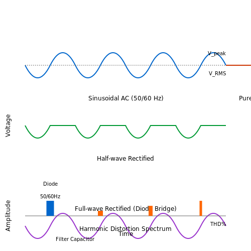
Alternating current (AC) and direct current (DC) represent the two primary forms of electrical power transmission and distribution. The key distinction lies in the time-dependent behavior of voltage and current. In DC systems, the voltage remains constant with respect to time, whereas in AC systems, the voltage varies periodically, typically following a sinusoidal waveform:
where f is the frequency (50 Hz or 60 Hz in most power grids) and φ is the phase angle. The root-mean-square (RMS) value of an AC waveform, which quantifies its equivalent heating effect compared to DC, is given by:
Transmission Efficiency and Practical Considerations
AC dominates large-scale power distribution due to the efficiency of voltage transformation using transformers. The power loss Ploss in a transmission line with resistance R and current I is:
By stepping up AC voltage to hundreds of kilovolts, the current—and thus resistive losses—are dramatically reduced. In contrast, DC requires power electronic converters (e.g., HVDC systems) for voltage transformation, which introduce switching losses but offer advantages for long-distance transmission due to the absence of reactive power and skin effect.
Rectification and Conversion
Most electronic devices operate internally on DC, necessitating AC-to-DC conversion. A full-wave rectifier with capacitive filtering produces a DC voltage approximating:
where C is the filter capacitance and Iload is the load current. Modern switched-mode power supplies (SMPS) achieve higher efficiency (>90%) through high-frequency AC conversion and regulation.
Historical Context and Modern Applications
The late 19th century "War of Currents" between Edison's DC and Tesla/Westinghouse's AC systems was ultimately decided by AC's superior transmission capabilities. Today, DC has resurged in:
- Renewable energy systems (solar panels produce DC natively)
- Data center power distribution (reducing conversion losses)
- Electric vehicle fast charging (350 kW+ DC chargers)
Harmonic Distortion and Power Quality
Nonlinear loads in AC systems introduce harmonic currents that distort the voltage waveform. Total harmonic distortion (THD) is quantified as:
where Vh is the RMS voltage of harmonic h. Power factor correction circuits and active filtering mitigate these effects in modern AC-DC converters.
2. Basic Operation and Components
2.1 Basic Operation and Components
Fundamental Power Supply Architecture
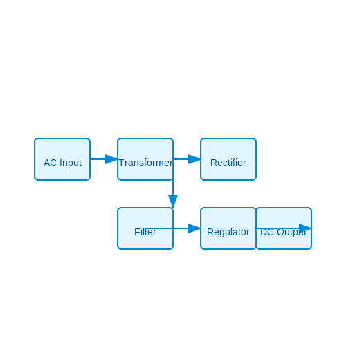
A power supply converts electrical energy from a source into a stable, regulated form suitable for powering electronic circuits. The primary components include:
- Transformer – Steps AC voltage up or down while providing galvanic isolation.
- Rectifier – Converts AC to pulsating DC, typically using diodes in half-wave, full-wave, or bridge configurations.
- Filter – Smoothes the rectified waveform using capacitors and/or inductors to reduce ripple.
- Regulator – Maintains a constant output voltage despite input variations or load changes.
Rectification and Filtering
For a full-wave rectifier with capacitive filtering, the ripple voltage Vr can be derived from the discharge equation of the filter capacitor:
where Iload is the load current, f is the ripple frequency (twice the input frequency for full-wave rectification), and C is the filter capacitance. The peak-to-peak ripple is minimized by increasing C or decreasing the load current.
Voltage Regulation
Linear regulators operate in the active region of a transistor to drop excess voltage, dissipating power as heat. The efficiency η of a linear regulator is given by:
Switching regulators, in contrast, achieve higher efficiency by rapidly switching a transistor between cutoff and saturation, storing energy in inductors or capacitors. The buck converter, for example, steps down voltage with efficiency often exceeding 90%:
where D is the duty cycle of the switching signal.
Practical Considerations
Real-world power supplies must account for:
- Transient response – The regulator's ability to maintain output during sudden load changes.
- Thermal design – Heat sinks or forced cooling may be necessary to dissipate wasted power.
- Electromagnetic interference (EMI) – Switching supplies require careful filtering to suppress high-frequency noise.
2.2 Advantages and Limitations
Linear Power Supplies
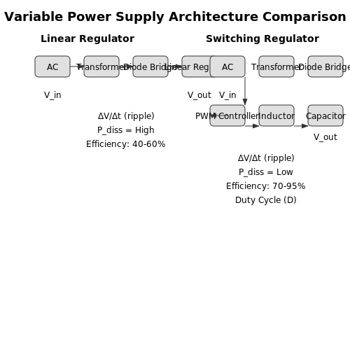
Linear power supplies offer low output noise and high stability, making them ideal for precision analog circuits. The absence of high-frequency switching eliminates electromagnetic interference (EMI), which is critical in sensitive measurement equipment. However, their efficiency is limited by the voltage drop across the series pass transistor, given by:
For example, a 5V output from a 12V input yields only ~41.7% efficiency. This inefficiency leads to significant heat dissipation, necessitating large heatsinks and increasing system volume.
Switching Power Supplies
Switch-mode power supplies (SMPS) achieve efficiencies exceeding 90% by rapidly switching transistors between saturation and cutoff states. Power loss is minimized since:
where D is duty cycle and fsw is switching frequency. However, SMPS introduce high-frequency ripple (typically 10-100mV) and require complex EMI filtering. The nonlinear switching action also generates harmonics that can interfere with nearby circuits.
Battery-Based Systems
Batteries provide galvanic isolation and portability but suffer from capacity fade governed by Peukert's law:
where k ranges from 1.1 to 1.3 for lead-acid batteries. Lithium-ion variants offer higher energy density (~250Wh/kg) but require protection circuits to prevent thermal runaway during overcharge.
Supercapacitor Hybrids
Ultracapacitors bridge the gap between batteries and conventional capacitors, with energy density (5-50Wh/kg) and power density (>10kW/kg). Their terminal voltage varies linearly with state of charge:
This characteristic necessitates DC-DC converters for voltage regulation, adding complexity to energy storage systems.
Regenerative Power Supplies
Used in motor drive and grid-tie applications, regenerative supplies can recover braking energy with efficiency:
However, they require bidirectional converters and sophisticated synchronization circuits for grid interconnection, increasing cost and control complexity.
2.3 Applications in Low-Noise Environments
Low-noise power supplies are critical in precision instrumentation, RF systems, and quantum computing, where even microvolt-level noise can corrupt measurements or disrupt sensitive signals. The primary challenge lies in minimizing both conducted and radiated noise while maintaining high efficiency and stability.
Noise Sources in Power Supplies
Switching regulators introduce high-frequency ripple due to their pulsed operation, while linear regulators generate thermal noise and flicker (1/f) noise. The total output noise Vn can be modeled as:
where Vth is thermal noise (4kTRB), Vsw is switching noise, and Vflicker is frequency-dependent flicker noise. For a 100 kHz buck converter with 10 mΩ output impedance, switching noise dominates above 1 MHz:
Noise Reduction Techniques
1. Linear Post-Regulation
Cascading a low-dropout (LDO) regulator after a switching stage attenuates high-frequency noise. The LDO's power supply rejection ratio (PSRR) must exceed:
For example, reducing 50 mV ripple to 5 μV requires 80 dB PSRR at the switching frequency.
2. Active Noise Cancellation
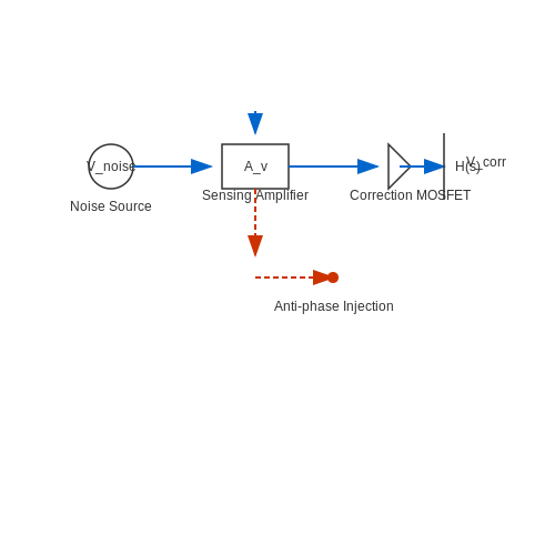
Feedforward techniques inject anti-phase noise to cancel supply perturbations. A typical implementation uses a sensing amplifier and correction MOSFET:
where H(s) is the transfer function matching the noise path delay.
Grounding and Layout Considerations
Star grounding prevents ground loops in mixed-signal systems. The critical parameter is ground impedance Zg:
For a 1 oz copper PCB at 100 MHz, 10 mm traces exhibit 25 mΩ resistance and 6 nH inductance, creating 3.8 Ω impedance.
Case Study: Cryogenic Readout Electronics
Quantum computing systems require power supplies with sub-nV/√Hz noise at 4K temperatures. Superconducting filters achieve 120 dB rejection above 10 MHz, but require careful thermal management to avoid microphonics.
3. How Switching Regulators Work
How Switching Regulators Work
Switching regulators, also known as switch-mode power supplies (SMPS), efficiently convert electrical power by rapidly switching a transistor between its saturation and cutoff states. Unlike linear regulators, which dissipate excess power as heat, switching regulators achieve high efficiency by minimizing power loss through controlled switching.
Basic Operating Principle
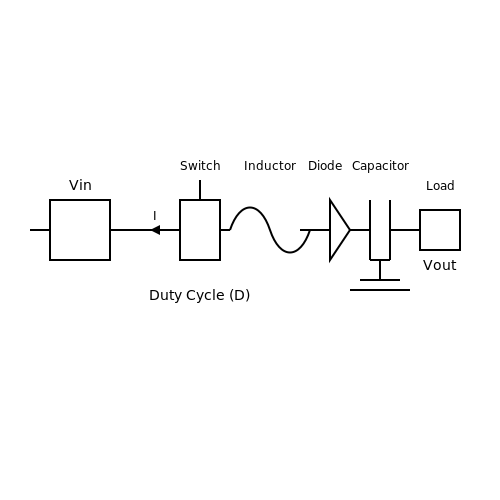
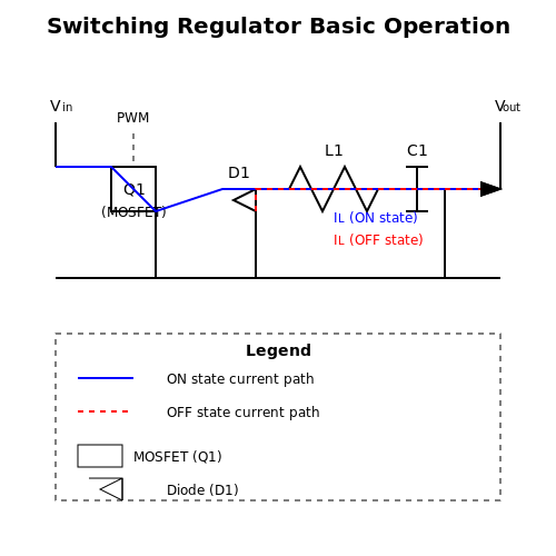
A switching regulator operates by storing energy in an inductor or capacitor during the on phase of the switch and releasing it during the off phase. The output voltage is regulated by adjusting the duty cycle (D) of the switching signal, defined as the ratio of the on-time to the total switching period (T):
For a buck (step-down) converter, the output voltage (Vout) is directly proportional to the duty cycle and input voltage (Vin):
Conversely, a boost (step-up) converter produces an output voltage higher than the input:
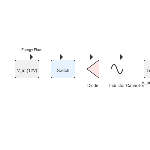
Key Components and Their Roles
A typical switching regulator consists of:
- Power switch (MOSFET/BJT): Rapidly toggles between on and off states to control energy transfer.
- Inductor: Stores energy during the switch's on-state and releases it during the off-state.
- Diode (or synchronous rectifier): Provides a path for inductor current when the switch is off.
- Output capacitor: Filters high-frequency ripple to produce a stable DC voltage.
- Control circuitry (PWM modulator): Adjusts the duty cycle based on feedback to maintain regulation.
Continuous vs. Discontinuous Conduction Modes
Switching regulators operate in two primary conduction modes:
- Continuous Conduction Mode (CCM): The inductor current never reaches zero within a switching cycle. This mode is common in high-power applications and provides lower output ripple.
- Discontinuous Conduction Mode (DCM): The inductor current drops to zero before the next switching cycle begins. DCM is often used in light-load conditions for improved efficiency.
The boundary between CCM and DCM is determined by the critical inductance (Lcrit):
where fsw is the switching frequency and Rload is the load resistance.
Efficiency and Loss Mechanisms
The efficiency (η) of a switching regulator is given by:
Major sources of power loss include:
- Switching losses: Occur during transistor turn-on/turn-off due to finite transition times.
- Conduction losses: Result from resistive losses in the switch, inductor, and PCB traces.
- Gate drive losses: Power dissipated in charging/discharging the transistor gate capacitance.
- Diode forward voltage drop: Particularly relevant in non-synchronous designs.
Modern designs mitigate these losses through synchronous rectification, zero-voltage switching (ZVS), and advanced semiconductor materials like GaN and SiC.
Control Techniques
Switching regulators employ various control methods to maintain output regulation:
- Voltage-mode control: Adjusts duty cycle based on output voltage feedback.
- Current-mode control: Uses both output voltage and inductor current feedback for improved transient response.
- Hysteretic (bang-bang) control: A simpler method where the output voltage oscillates within a defined window.
The choice of control method affects stability, transient response, and noise immunity. Compensation networks are often required to ensure stability across load conditions.
Practical Considerations
Designing a high-performance switching regulator requires attention to:
- PCB layout: Minimizing parasitic inductance and resistance in high-current paths.
- Thermal management: Ensuring adequate heat dissipation for power components.
- EMI mitigation: Proper filtering and shielding to reduce conducted and radiated emissions.
- Component selection: Choosing inductors, capacitors, and switches with appropriate ratings.
Modern integrated regulator ICs often incorporate many of these considerations, simplifying design while maintaining high performance.
3.2 Efficiency and Thermal Considerations
Power Conversion Efficiency
The efficiency η of a power supply is defined as the ratio of output power Pout to input power Pin:
For switched-mode power supplies (SMPS), typical efficiencies range from 70% to 95%, while linear regulators achieve only 30-60% due to their dissipative operation. The primary loss mechanisms include:
- Conduction losses in semiconductors and passive components
- Switching losses during transistor transitions
- Magnetic core losses in transformers and inductors
- Gate drive losses in power MOSFETs/IGBTs
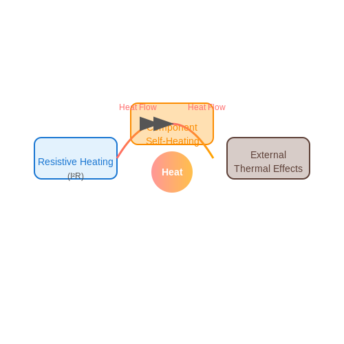
Thermal Analysis and Heat Dissipation
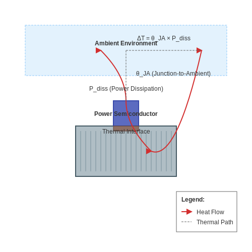
Power dissipation Pdiss generates heat according to:
The resulting temperature rise depends on the thermal resistance θJA (junction-to-ambient):
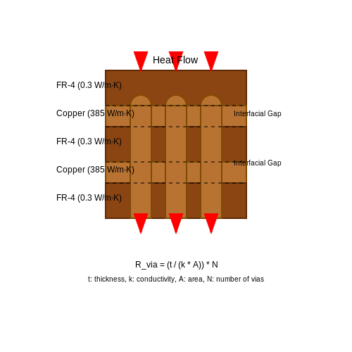
For example, a 100W power supply with 85% efficiency dissipating 15W through a heatsink with θJA = 2°C/W will experience a 30°C temperature rise above ambient.
Thermal Management Techniques
Effective cooling strategies include:
- Heatsink design: Optimizing fin geometry and surface area
- Forced air cooling: Using fans to enhance convection
- Thermal interface materials: Reducing contact resistance
- PCB layout: Utilizing thermal vias and copper pours
Efficiency Optimization Methods
Advanced techniques to improve efficiency:
Where ηi represents the efficiency of each power stage. Key optimization approaches include:
- Synchronous rectification in DC-DC converters
- Zero-voltage switching (ZVS) and zero-current switching (ZCS)
- Adaptive gate drive voltage control
- Digital control for optimal switching timing
Practical Design Considerations
In high-power applications, thermal cycling affects reliability through:
Where Nf is the number of cycles to failure, A is a material constant, Ea is activation energy, and n is the Coffin-Manson exponent. Designers must balance efficiency improvements against:
- Component derating requirements
- Thermal expansion mismatches
- Cooling system complexity
- Cost-performance tradeoffs
3.3 Common Topologies: Buck, Boost, and Buck-Boost
Buck Converter
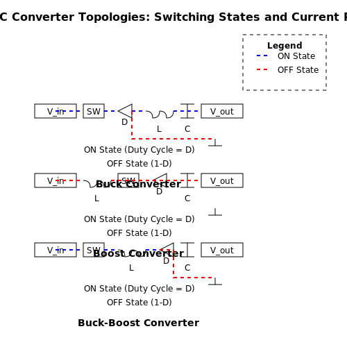
The buck converter is a step-down DC-DC converter that efficiently reduces input voltage while maintaining high efficiency. Its operation relies on pulse-width modulation (PWM) to control the duty cycle (D) of the switching transistor, typically a MOSFET. The output voltage (Vout) is given by:
When the switch is closed (on-state), energy is stored in the inductor, and the diode is reverse-biased. During the off-state, the inductor releases energy through the diode to the load. The inductor current ripple (ΔIL) is critical for stability and is derived as:
where L is the inductance and fsw is the switching frequency. Buck converters are widely used in voltage regulators, battery chargers, and point-of-load (POL) applications.
Boost Converter
The boost converter steps up the input voltage, making it essential for applications like LED drivers and renewable energy systems. Its output voltage is determined by:
During the on-state, the inductor stores energy while the diode blocks current flow to the load. In the off-state, the inductor voltage adds to the input voltage, forcing current through the diode to the output capacitor. The inductor current ripple is:
Boost converters require careful design to avoid discontinuous conduction mode (DCM), which increases output voltage ripple and reduces efficiency.
Buck-Boost Converter
The buck-boost converter provides flexibility by either stepping up or stepping down the input voltage, with a polarity inversion. The output voltage is expressed as:
During the on-state, the inductor charges while the diode isolates the load. In the off-state, the inductor discharges through the diode, transferring energy to the output. The inductor current ripple is similar to the boost converter but must account for bidirectional energy flow:
Buck-boost converters are ideal for battery-powered systems where input voltage varies widely, such as in portable electronics and automotive applications.
Comparative Analysis
- Efficiency: Buck converters typically achieve >90% efficiency due to lower switching losses. Boost and buck-boost converters suffer from higher diode conduction losses.
- Output Ripple: Buck converters exhibit lower ripple due to LC filtering. Boost and buck-boost topologies require larger capacitors to mitigate ripple.
- Applications: Buck converters dominate fixed-voltage applications, while boost and buck-boost are preferred for dynamic input ranges.
Practical Design Considerations
Key parameters for optimizing these topologies include:
- Switching Frequency (fsw): Higher frequencies reduce inductor size but increase switching losses.
- Inductor Selection: Must handle peak current without saturation while minimizing core losses.
- Diode/Transistor Choice: Schottky diodes and MOSFETs with low RDS(on) improve efficiency.
Modern ICs integrate these components with advanced control schemes (e.g., current-mode control) to enhance performance and reliability.
4. Load Regulation and Line Regulation
4.1 Load Regulation and Line Regulation
Definition and Significance
Load regulation measures a power supply's ability to maintain a stable output voltage despite variations in the load current. Conversely, line regulation quantifies the power supply's stability against fluctuations in the input voltage. Both parameters are critical in applications requiring precise voltage delivery, such as laboratory instruments, medical devices, and high-performance computing systems.
Mathematical Formulation
Load regulation is expressed as a percentage and derived from the no-load (VNL) and full-load (VFL) output voltages:
Line regulation is similarly defined, but considers input voltage variations (ΔVin) and their effect on the output (ΔVout):
Practical Implications
Poor load regulation manifests as voltage droop under high current loads, potentially destabilizing sensitive circuits. Line regulation deficiencies lead to output variations when the input supply (e.g., AC mains) experiences sags or surges. Modern switching regulators typically achieve <0.1% load regulation and <0.01% line regulation through feedback control loops.
Measurement Techniques
Load regulation testing involves sweeping the output current from minimum to maximum while monitoring voltage deviations. Line regulation testing requires varying the input voltage across its specified range (e.g., 90-264V AC for universal inputs) with a constant load. Automated test systems often employ programmable electronic loads and data acquisition units for precision measurements.
Design Considerations
Three key factors influence regulation performance:
- Feedback loop bandwidth: Higher bandwidth improves transient response but risks instability
- Reference voltage stability: Temperature-compensated references (e.g., bandgap) minimize drift
- Power stage impedance: Lower output impedance reduces load-induced voltage variations
Advanced designs may incorporate feedforward compensation to anticipate input voltage changes or nonlinear control techniques like hysteresis for improved transient response.
4.2 Protection Circuits: Overvoltage, Overcurrent, and Short-Circuit
Overvoltage Protection
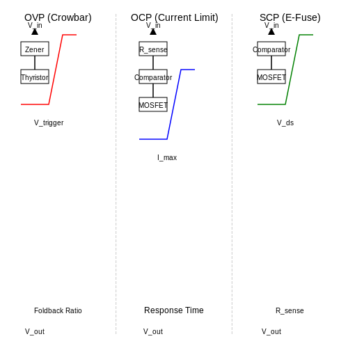
Overvoltage protection (OVP) circuits safeguard electronic systems from voltage spikes exceeding predefined thresholds. A common implementation involves a crowbar circuit, which rapidly shunts excess voltage to ground when triggered. The core components include a zener diode or voltage reference IC to detect overvoltage, and a thyristor or SCR to discharge the supply.
where \( V_z \) is the zener breakdown voltage and \( V_{gate(th)} \) is the thyristor's gate threshold. For precision applications, integrated OVP ICs like the LT4356 provide adjustable thresholds with response times under 1µs.
Overcurrent Protection
Overcurrent protection (OCP) limits current flow to prevent thermal damage. Two dominant methodologies exist:
- Current Limiting: Uses a sense resistor (\( R_{sense} \)) and comparator to modulate a pass transistor (e.g., MOSFET). The current limit \( I_{max} \) is given by:
- Foldback Current Limiting: Reduces current further during sustained faults, minimizing power dissipation. The foldback characteristic is defined by:
Short-Circuit Protection
Short-circuit protection (SCP) must react within milliseconds to prevent catastrophic failure. Electronic fuses (e-fuses) combine OCP with fast-acting MOSFET disconnection. The response time \( t_{response} \) depends on the gate capacitance \( C_{gs} \) and drive current \( I_{drive} \):
Advanced implementations use desaturation detection in IGBTs or MOSFETs, where a fault is flagged when \( V_{ds} \) exceeds a threshold during conduction.
Practical Considerations
Protection circuits introduce tradeoffs:
- False Triggering: Noise immunity requires hysteresis in comparator-based designs.
- Latency vs. Safety: Faster response increases transient susceptibility.
- Recovery Behavior: Latching vs. auto-retry modes impact system availability.
For high-reliability systems, redundancy (e.g., dual OVP/OCP stages) and fault simulations in SPICE or PLECS are recommended.
4.3 Filtering and Noise Reduction Techniques
Fundamentals of Power Supply Noise
Noise in power supplies arises from multiple sources, including switching transients, rectifier diode reverse recovery, and electromagnetic interference (EMI). The primary contributors are:
- Ripple voltage due to incomplete smoothing of rectified AC.
- Switching noise from high-frequency DC-DC converters.
- Conducted and radiated EMI coupling into supply lines.
Quantitatively, ripple voltage in a capacitor-input filter can be expressed as:
where \( I_{load} \) is the load current, \( f \) is the ripple frequency, and \( C \) is the filter capacitance.
Passive Filtering Techniques
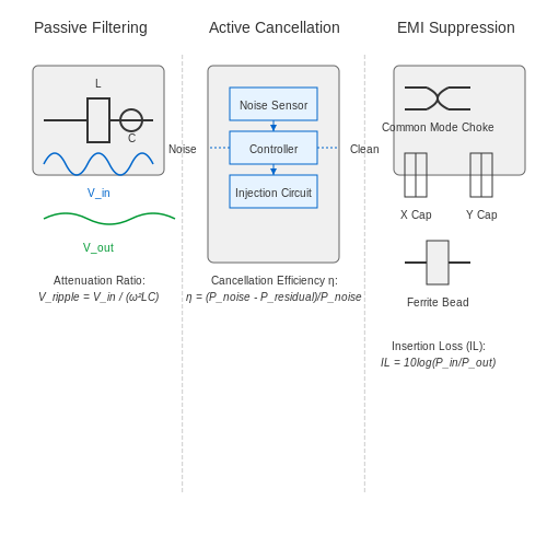
Passive LC filters remain the most widely used solution for ripple attenuation. The attenuation ratio of a second-order LC filter is given by:
For optimal performance:
- Choose inductors with low DC resistance (DCR) to minimize voltage drop.
- Select capacitors with low equivalent series resistance (ESR) for high-frequency bypassing.
- Implement multi-stage filtering for broadband attenuation.
Active Noise Cancellation
Active ripple cancellation circuits inject an anti-phase signal to nullify noise. The most effective implementations use:
- Operational amplifiers in differential configurations.
- Current-sensing feedback loops with bandwidths exceeding the noise spectrum.
- Adaptive algorithms for variable-frequency switching regulators.
The cancellation efficiency \( \eta \) depends on the phase matching accuracy:
EMI Suppression Methods
For conducted EMI above 150 kHz, three primary techniques prove effective:
- Common-mode chokes: Present high impedance to differential noise while allowing DC current.
- X/Y capacitors: Provide low-impedance paths for high-frequency noise to ground.
- Ferrite beads: Act as frequency-dependent resistors attenuating RF noise.
The insertion loss of an EMI filter follows:
Advanced Techniques
For sensitive instrumentation applications, consider:
- Cascaded active-passive hybrids: Combine the broadband performance of LC filters with active cancellation.
- Digital adaptive filtering: Use DSP algorithms to identify and suppress noise spectra in real-time.
- Superconducting filters: Provide near-ideal frequency selectivity for ultra-low-noise systems.
Practical Implementation Considerations
When designing noise reduction systems:
- Maintain proper grounding schemes to avoid ground loops.
- Minimize parasitic inductances in high-speed switching paths.
- Use proper PCB layout techniques (e.g., star grounding, guard rings).
- Verify performance with spectrum analyzer measurements.
5. Digital Power Management and Control
5.1 Digital Power Management and Control
Fundamentals of Digital Power Control
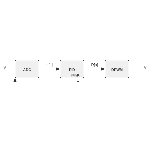
Digital power management replaces traditional analog control loops with microprocessor-based systems, enabling precise regulation, adaptive tuning, and real-time monitoring. Unlike analog controllers, which rely on fixed passive components, digital implementations use software algorithms to dynamically adjust control parameters such as proportional-integral-derivative (PID) coefficients, switching frequencies, and feedback gains.
where Kp, Ki, and Kd are the PID coefficients, Ts is the sampling period, and z represents the Z-transform domain. This discrete-time implementation allows for real-time optimization through adaptive algorithms.
Key Architectures and Topologies
Modern digital power supplies employ one of three primary control architectures:
- Voltage-Mode Control (VMC): The output voltage is directly regulated using a single feedback loop. While simple, it suffers from slow transient response.
- Current-Mode Control (CMC): Uses an inner current loop and outer voltage loop, improving dynamic response but requiring careful slope compensation.
- Hysteretic Control: A nonlinear method where the output switches when crossing predefined voltage thresholds, offering ultra-fast response but variable frequency operation.
Digital Pulse-Width Modulation (DPWM)
DPWM replaces analog comparators with high-resolution timers and counters. The duty cycle D is computed digitally:
where e[n] is the error signal at the nth sample, and K, Ki are control gains. Advanced implementations use ΔΣ modulation to achieve sub-nanosecond resolution.
Real-World Applications
Digital control is dominant in:
- Server Power Delivery: Intel’s VR13 standard mandates digital multiphase controllers for CPUs, achieving >90% efficiency at 500A load steps.
- Renewable Energy: Maximum Power Point Tracking (MPPT) in solar inverters uses perturb-and-observe algorithms running on DSPs.
- Automotive: Tesla’s 48V battery systems employ predictive current control to minimize EMI in high-noise environments.
Challenges and Mitigations
Key limitations include:
- Quantization Noise: Finite ADC/DAC resolution introduces step artifacts, mitigated via dithering or higher bit-depth converters.
- Loop Latency: Computational delay degrades phase margin; solutions include pipelined algorithms or FPGA-based implementations.
- EMI Susceptibility: Clock jitter can modulate switching noise, addressed through spread-spectrum techniques.
5.2 Energy Harvesting and Renewable Power Integration
Fundamentals of Energy Harvesting
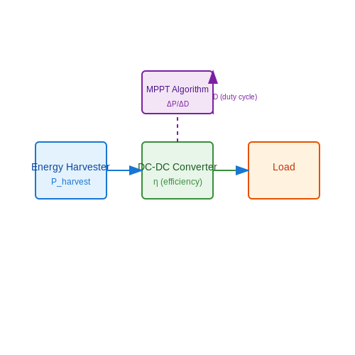
Energy harvesting involves capturing ambient energy from the environment—such as solar, thermal, vibrational, or RF sources—and converting it into usable electrical power. The efficiency of an energy harvesting system is determined by the transduction mechanism and power conditioning circuitry. For a given source, the extractable power Pharvest is constrained by the source's energy density and the harvester's conversion efficiency η:
where A is the effective harvesting area and Esource is the energy density of the ambient source. For instance, solar irradiance typically provides 100–1000 W/m², while vibrational energy ranges from 0.1–10 mW/cm³.
Power Conversion and Maximum Power Point Tracking (MPPT)
To optimize energy extraction, impedance matching between the harvester and load is critical. Maximum Power Point Tracking (MPPT) algorithms dynamically adjust the load impedance to maintain operation at the peak power point. A common approach uses perturb-and-observe (P&O) to iteratively adjust the duty cycle D of a DC-DC converter:
where ΔP is the power change resulting from a small duty cycle perturbation ΔD. Advanced implementations employ fractional open-circuit voltage or conductance-based methods for faster convergence.
Renewable Integration Challenges
Integrating intermittent renewable sources with conventional power grids or battery systems requires:
- Power smoothing using supercapacitors or flywheels to mitigate fluctuations.
- Islanding detection to prevent grid-tied inverters from energizing disconnected grids.
- Bidirectional converters for hybrid systems combining solar, wind, and storage.
The stability of such systems is analyzed via small-signal modeling of the power electronics interface. For a grid-tied inverter, the output impedance Zout must satisfy the Nyquist criterion relative to the grid impedance Zgrid to avoid resonance.
Case Study: Solar-Wind Hybrid System
A practical implementation might combine a 200 W photovoltaic array with a 300 W vertical-axis wind turbine. The power curves are complementary—solar peaks at midday, while wind often increases at night. The combined DC output is fed through a dual-input buck-boost converter with MPPT for each source:
Such systems achieve >85% efficiency in field deployments, with Li-ion batteries providing overnight storage.
5.3 Miniaturization and High-Density Power Solutions
The relentless demand for smaller, more efficient power supplies has driven innovations in miniaturization and high-density power conversion. Modern applications—ranging from portable electronics to aerospace systems—require power solutions that deliver high efficiency while occupying minimal volume. Key challenges include thermal management, electromagnetic interference (EMI), and maintaining efficiency at reduced scales.
Fundamentals of Miniaturization
Miniaturization hinges on increasing power density (W/cm³), which is achieved through:
- Higher switching frequencies to reduce passive component sizes.
- Advanced semiconductor materials (e.g., GaN, SiC) for lower conduction and switching losses.
- Multilayer PCB designs integrating magnetics and capacitors.
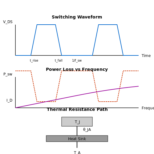
The power density of a converter can be expressed as:
where \( P_{\text{out}} \) is the output power and \( V_{\text{total}} \) is the total volume of the converter.
High-Frequency Switching and Loss Mechanisms
Operating at higher frequencies (MHz range) reduces the size of inductors and capacitors but introduces trade-offs:
- Switching losses increase due to faster transitions, governed by:
where \( t_{\text{rise}} \) and \( t_{\text{fall}} \) are the switching times, and \( f_{\text{sw}} \) is the switching frequency.
- Skin and proximity effects increase AC resistance in conductors, necessitating planar magnetics or Litz wire.
Thermal Management in High-Density Designs
Heat dissipation becomes critical as power density increases. The thermal resistance \( \theta_{JA} \) (junction-to-ambient) must be minimized through:
- Embedded heat sinks or thermal vias in PCBs.
- Liquid cooling or phase-change materials in extreme cases.
The junction temperature \( T_J \) is calculated as:
where \( T_A \) is the ambient temperature and \( P_{\text{loss}}} \) is the total power loss.
Advanced Packaging Techniques
3D packaging and system-in-package (SiP) technologies enable tighter integration:
- Flip-chip bonding reduces parasitic inductance.
- Embedded die technologies place power ICs within PCB layers.
For example, a GaN-based buck converter can achieve power densities exceeding 300 W/cm³ using these methods.
Case Study: Aerospace Power Modules
In aerospace applications, weight and volume constraints necessitate ultra-high-density designs. A 1 kW, 48 V-to-12 V converter might use:
- GaN HEMTs switching at 5 MHz.
- Planar transformers with integrated cooling.
- Ceramic capacitors for high-frequency decoupling.
Such designs achieve efficiencies above 95% while fitting within a 2 cm × 2 cm footprint.
Future Directions
Emerging trends include:
- Wide-bandgap (WBG) devices pushing frequencies beyond 10 MHz.
- AI-optimized layout algorithms for thermal and EMI performance.
- Additive manufacturing of power components.
6. Recommended Books and Publications
6.1 Recommended Books and Publications
- PDF Power Sources and Supplies: World Class Designs — Power sources and supplies/Marty Brown. p. cm.—(Newnes world class designs series) Includes bibliographical references and index. ISBN-13: 978--7506-8626-6 (pbk. : alk. paper) 1. Electric power supplies to apparatus—Design and construction. 2. Electric apparatus and appliances—Power supply. I. Title. TK7868.P6B758 2007 621.317—dc22 ...
- PDF Power Electronics and Electric Drives - download.e-bookshelf.de — 5.5 Railway power supply system 276 5.6 ESSs for railway applications 278 5.7 Ground level power supply systems 332 5.8 Auxiliary power systems for railway applications 338 5.9 Real examples 340 5.10 Historical evolution 351 5.11 New trends and future challenges 351 References 357 6 Ships 362 Iñigo Atutxa and Gonzalo Abad 6.1 Introduction 362
- PDF Series for Design Engineers - WordPress.com — 1. The Role of the Power Supply within the System and the Design Program 1.1 Getting Started. This Journey Starts with the First Question 1 1.2 Power System Organization 2 1.3 Selecting the Appropriate Power Supply Technology 3 1.4 Developing the Power System Design Specification 5 1.5 A Generalized Approach to Power Supplies: Introducing the
- Power Sources and Supplies: World Class Designs — Purchase Power Sources and Supplies: World Class Designs - 1st Edition. Print Book & E-Book. ISBN 9780750686266, 9780080556574 ... a leader in the field of power design to select the very best design-specific material from the Newnes portfolio. ... and its real-world approach to design issues. Special attention is given to switching power ...
- DC Power Supplies: Power Management and Surge Protection for Power ... — A summary of underlying principles and essential design points, it compares academic research and industry publications and reviews DC power supply fundamentals, including linear and low-dropout regulators. ... Best Sellers Rank: #8,202,344 in Books ... He has authored ten books for practicing electronic engineers including the two consecutive ...
- 6 - ELECTRONIC POWER SUPPLIES - Cambridge University Press & Assessment — book contents. frontmatter; contents; preface; 1 electronic systems: a century of progress; 2 the semiconductor junction diode: the basis of modern electronics; 3 the bipolar junction transistor: an active electronic device; 4 the metal-oxide field-effect transistor: another active device; 5 negative feedback and operational amplifiers; 6 electronic power supplies; appendix a fabrication of ...
- PDF CHAPTER 6 Switch-Mode Powe - Springer — CHAPTER 6 Switch-Mode Power Supplies 6.1 Introduction 6.1.1 Development of DC Power Supplies DC power supplies -either regulated or not are needed in industrial equip ment, in o
- 6 Power Supply Design - Practical Electronic Design for Experimenters ... — CHAPTER 6Power Supply Design Every electronic product needs a power supply. All electronic circuits rely on one or more dc voltage sources for power. As a result, any design … - Selection from Practical Electronic Design for Experimenters [Book] ... O'Reilly members experience books, live events, courses curated by job role, and more from O ...
- PDF Design Guide: Designing and Building High Voltage Power Supplies ... - DTIC — guidelines for improving both high voltage and low voltage power supplies for the U.S. Air Force systems command. It is the intent of the report to supply good design and manufac-turing techniques for the packaging and the building of high quality, reliable, long-life power supplies.
- Power Sources and Supplies: World Class Designs - O'Reilly Media — This is a book that belongs on the workbench of every power supply designer! *Marty Brown, author and power supply design consultant, has personally selected all content for its relevance and usefulness *Covers best design practices for switching power supplies and power converters *Emphasis is on pragmatic solutions to commonly encountered ...
6.2 Online Resources and Datasheets
- PDF EPS12V Power Supply Design Guide - TechPowerUp — EPS12V Power Supply Design Guide, V2.92 - 7 - 1 2 Purpose This specification defines a non-redundant power supply that supports entry server computer systems. Recommendations for 550 W, 600 W, 650 W, 700W, 750W, 800W, 850W, and 950W power supplies with up to 9 outputs (3.3 V, 5 V, 12V1, 12V2, 12V3, 12V4, 12V5, -12 V, and 5 VSB) are provided.
- PDF HPF-PS6/HPF-PS10 Series 6/10 Amp, 24 Volt Power Supplies - Notifier — HPF-PS6/HPF-PS10 Series 6/10 Amp, 24 Volt Power Supplies General The HPF-PS Series is a remote power supply line from Honeywell and is a direct replacement for the PSE and FCPS Series. The HPF-PS6(B)(E) is a 6 amp and the HPF-PS10(B)(E) is a 10 amp, remote power supply with battery charger that may be connected to
- Find Datasheets, Electronic Parts, Components - Datasheets.com — Datasheets.com is the easiest search engine to find datasheets of electronic parts. Search millions of components across thousands of manufacturers. Datasheets. Part Explorer; Manufacturers; Tools/Calculators ... 6 Using for STR-W6756 Universal-input 140 W power supply by: Allegro MicroSystems. TAS5508-5122C6EVM, Evaluation Kit for TAS5508 ...
- Electronics Datasheets - Parts Search and Technical Documents — Power supply reference design for Horizon Robotics Journey 5 with one PMIC. Evaluation Kits ... Your Source for Online Electronic Component Datasheets. We give you instant and unrestricted access to a comprehensive resource of datasheets and other technical documents from our growing database of electronics parts, sourced directly from the top ...
- PDF Linear Power Supplies Data Sheet - RS Components — MCD10016 Rev. 1.2, 13-Nov-09 Page 2 of 9 www.power-one.com Linear Power Supplies Data Sheet (See Additional Features Column) A Overvoltage protection, set at 6.2 V ±0.4 V. B Non-adjustable 3-terminal regulator. C Remote sense provided. D With output inhibit and parallel operation master/slave capability. E With output inhibit.
- Download Power Supply Datasheets | Acopian Power Supplies — Whatever you prefer to call it - power supply, rectifier, power system, power module, power brick - we make millions of different kinds that can be used in thousands of different applications including electronic equipment, manufacturing, machinery, process control, factory automation, astrophysics, chemical processing, telecommunications, monitoring systems, audio, scientific research ...
- PDF Series for Design Engineers - WordPress.com — 1. The Role of the Power Supply within the System and the Design Program 1.1 Getting Started. This Journey Starts with the First Question 1 1.2 Power System Organization 2 1.3 Selecting the Appropriate Power Supply Technology 3 1.4 Developing the Power System Design Specification 5 1.5 A Generalized Approach to Power Supplies: Introducing the
- Programmable DC Power Supplies - TDK Product Center — Electronics ABC (TECH-MAG) Guidebook for EMC. Environment. Environment ... Data Sheet ; User Manual ; IEEE User Manual ; LAN Interface Manual ... Programmable DC Power Supplies. 1U Rack Mount, Output: 1680W, 0 to 600V Blank front panel (ATE version) GEN 1500-10-3P208 ...
- PDF AN-556Introduction to Power Supplies - Texas Instruments — An ideal power supply would be characterized by supplying a smooth and constant output voltage regardless of variations in the voltage, load current or ambient temperature at 100% conversion efficiency. Figure 1 compares a real power supply to this ideal one and further illustrates some power supply terms. Figure 1.
- PDF Target Areas Description - Arduino Docs — 5.2 Power Specification Property Min Typ Max Unit Supply voltage 7.0 - 12 V Permissible range 6.0 - 16 V Safety Note: Unlike most traditional Arduino boards, the Arduino Due board runs at 3.3 V. Keep in mind the maximum voltage that the I/O pins can tolerate is 3.3 V. Applying voltages higher than 3.3 V to any I/O pin could damage the board.
6.3 Industry Standards and Compliance Guidelines
- Power Supply EMC Compliance Standards - Snaptec — AS/NZS 4251.1: 1999 Electromagnetic compatibility (EMC) Generic emission standard Part 1: Residential, commercial and light industry AS/NZS 61000.6.3: 2007 Electromagnetic compatibility (EMC) Part 6.3: Generic standards Emission standard for residential, commercial and light industrial environments EN 61000 6 3: 2001 with amendment A11 (2004) Electromagnetic compatibility (EMC) Part 6 3 ...
- IEC 61000-6-3 - Electromagnetic compatibility (EMC) - Part 6-3: Generic ... — IEC 61000-6-3:2020 is a generic EMC emission standard applicable only if no relevant dedicated product or product family EMC emission standard has been published. This part of IEC 61000 for emission requirements applies to electrical and electronic equipment intended for use at residential (see 3.1.14) locations.
- PDF A Guide to United States Electrical and Electronic Equipment Compliance ... — Effective March 10, 2020, the DOE adopted a new energy conservation standard for uninterruptible power supplies, a class of battery chargers. Compliance with the new standard is required on and after January 10, 2022.
- List of common EMC test standards - Wikipedia — These standards attempt to standardize product EMC performance, with respect to conducted or radiated radio interference from electrical or electronic equipment, imposition of other types of disturbance on the mains supply by such equipment, and the sensitivity of such equipment to received interference.
- PDF performance and test requirements Part 3: Method of specifying the ... — This part of IEC 62040 establishes the performance and test requirements applied to movable, stationary and fixed electronic uninterruptible power systems (UPS) that
- PDF Electrical Power Requirements — Increase the power supply voltage from nominal rated voltage in incremental steps and monitor the corresponding power 'nd standard reference indicator levels. Cease testing when the standard reference indicator level falls outside of stated tolerances or the test item's overvoltage protection devices operate.
- PDF Microsoft Word - CE Marking paper final 9-7-18 - EPSMA — The European Power Supplies Manufacturers' Association was established in 1995 to represent the European power supply industry. Disclaimer: No responsibility or liability can be accepted by the EPSMA or any of its officers or members for the content of this guidance document, and the information contained herein should not be used as a ...
- PDF Disturbance Monitoring and Reporting Requirements — There are a variety of ways to capture the data PRC-002-2 addresses, and existing and currently available equipment can meet the requirements of this standard. PRC-002-2 also addresses the importance of addressing the availability of Disturbance monitoring capability to ensure the completeness of BES data capture.
- PDF FINAL Version 1.1 ENERGY STAR UPS Program Requirements — Direct Current (Dc)-output UPS/Rectifier: UPS that supplies power with a continuous flow of electric charge that is unidirectional. Includes both individual rectifier units for dc applications and entire Dc-output UPS frames or systems, consisting of rectifier modules, controllers, and any other supporting components.
- PDF Quality Requirements for DC Uninterruptible Power Systems (UPS ... - IOGP — The purpose of this quality requirements specification (QRS) is to define quality management requirements for the procurement of DC uninterruptible power systems (UPS) in accordance with IOGP S-702 for application in the petroleum and natural gas industries.