Zigzag Waveguide Structures
1. Definition and Basic Geometry
1.1 Definition and Basic Geometry
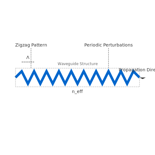
A zigzag waveguide is a periodic structure where the guiding channel follows a sawtooth or meandering path rather than a straight line. The geometry is characterized by alternating segments with fixed tilt angles ±θ, creating a corrugated propagation path. Unlike conventional waveguides, this structure introduces controlled discontinuities that modify the dispersion relation and enable unique modal properties.
Mathematical Parameterization
The fundamental geometric parameters of a zigzag waveguide include:
- Periodicity length (Λ): Distance between equivalent points in adjacent zigzag segments
- Tilt angle (θ): Angular deviation from the propagation axis (typically 10°-45°)
- Corner radius (rc): Curvature at bending points to minimize radiation losses
- Core width (w): Transverse dimension of the guiding region
where L is the straight segment length between bends. The effective index neff becomes spatially modulated due to the periodic path length variation:
Fabrication Considerations
Modern implementations typically use:
- Silicon-on-insulator (SOI) platforms with 220-300 nm silicon layers
- Deep UV or electron-beam lithography for sub-micron precision
- Anisotropic dry etching to achieve vertical sidewalls (>88°)
Modal Characteristics
The zigzag geometry couples forward and backward propagating modes through Bragg scattering. The phase matching condition occurs when:
where β is the propagation constant. This creates photonic bandgaps analogous to electronic semiconductors, with forbidden frequency ranges determined by the Floquet-Bloch theorem.
Applications
Zigzag waveguides enable several advanced photonic functions:
- Slow light enhancement in nonlinear optics (χ(2), χ(3) processes)
- Distributed feedback in semiconductor lasers
- Optical delay lines with tunable group velocity
- Polarization mode conversion
1.2 Historical Development and Applications
Early Theoretical Foundations
The concept of waveguides dates back to the late 19th century, with foundational work by Lord Rayleigh (1887) on electromagnetic wave propagation in hollow metallic tubes. However, the development of zigzag waveguide structures emerged much later, driven by the need for compact, low-loss transmission lines in microwave and optical systems. The first theoretical treatment of periodic corrugations in waveguides appeared in the 1950s, with researchers like R.E. Collin and J.R. Pierce analyzing the dispersion characteristics of periodically loaded transmission lines.
where β(ω) is the propagation constant, ωc is the cutoff frequency, and Δβperiodic accounts for the perturbation introduced by the zigzag geometry.
Technological Advancements
The 1970s saw experimental validation of zigzag waveguides in millimeter-wave systems, where their ability to suppress higher-order modes proved critical for satellite communications. Advances in microfabrication during the 1990s enabled photonic implementations, with silicon-on-insulator (SOI) platforms achieving sub-micron periodic perturbations for optical signal processing.
- Key milestones:
- 1968: First experimental demonstration of zigzag slow-wave structures in traveling-wave tubes
- 1983: Application in phased-array radar systems for beam steering
- 2005: Integration with photonic crystals for optical dispersion engineering
Modern Applications
Microwave Systems
In contemporary radar and 5G/6G systems, zigzag waveguides provide:
- Enhanced bandwidth through engineered dispersion
- Reduced cross-talk in dense antenna arrays
- Improved power handling via distributed impedance matching
Photonic Integrated Circuits
The periodic nature of zigzag structures enables:
where Λ is the zigzag period and neff is the effective refractive index. This principle underpins applications in:
- Tunable optical filters with >40 nm tuning range
- Nonlinear frequency conversion in χ(2) and χ(3) media
- Topological photonic insulators using synthetic dimensions
Quantum Technologies
Recent work exploits zigzag waveguides for:
- Entangled photon pair generation via spontaneous parametric down-conversion
- Superconducting qubit coupling in microwave quantum circuits
- Topologically protected edge states in photonic quantum walks
1.3 Comparison with Conventional Waveguides
Propagation Characteristics
Zigzag waveguides exhibit distinct propagation properties compared to conventional straight waveguides. The periodic bending introduces additional phase shifts, altering the effective refractive index. For a zigzag waveguide with bending angle θ and period Λ, the propagation constant βeff is modified as:
where β0 is the propagation constant of the straight waveguide. This results in a reduced group velocity, enhancing light-matter interaction for nonlinear applications.
Modal Confinement and Loss Mechanisms
Conventional waveguides rely on total internal reflection (TIR) for modal confinement, whereas zigzag structures introduce additional scattering losses at each bend. The radiation loss per unit length αrad can be approximated as:
where C is a geometry-dependent constant, w is the waveguide width, and λ is the wavelength. Despite higher losses, zigzag designs enable tighter bending radii (as low as 5λ) compared to conventional waveguides (typically >50λ).
Dispersion Engineering
The periodic perturbation in zigzag waveguides creates photonic bandgaps, enabling tailored dispersion profiles. The group velocity dispersion (GVD) parameter D is given by:
where neff is the effective index. Zigzag structures can achieve anomalous dispersion (D > 0) at visible wavelengths, unlike conventional waveguides that typically exhibit normal dispersion in this regime.
Fabrication Tolerance
Conventional waveguides require sub-nanometer smoothness for low-loss operation, while zigzag structures are more tolerant to sidewall roughness due to reduced overlap between the mode and waveguide edges. The scattering loss reduction factor η scales with bending angle:
where θc is the critical angle for TIR. This makes zigzag waveguides preferable for low-cost fabrication processes.
Applications in Integrated Photonics
- Slow-light devices: Enhanced light-matter interaction enables compact optical buffers
- Nonlinear optics: Higher power density facilitates frequency conversion
- Quantum photonics: Tailored dispersion supports entangled photon generation

2. Modes of Propagation
2.1 Modes of Propagation
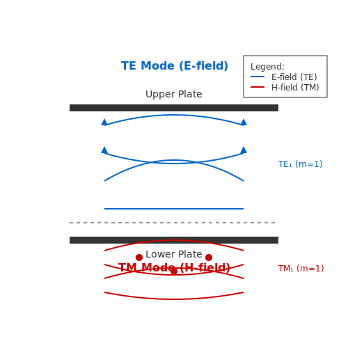
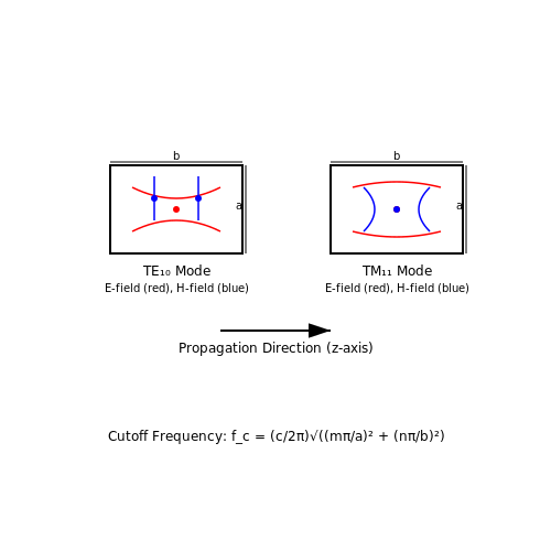
Zigzag waveguide structures exhibit unique modal properties due to their periodic geometric perturbations. The modes of propagation in such waveguides are fundamentally governed by Floquet-Bloch theory, where the periodicity of the structure imposes phase-matching conditions on the electromagnetic fields. Unlike straight waveguides, zigzag structures support hybrid modes that couple transverse electric (TE) and transverse magnetic (TM) components due to the broken symmetry.
Mathematical Formulation of Modal Fields
The electric and magnetic fields in a zigzag waveguide can be expressed as Bloch waves, taking the form:
where β is the propagation constant, ω is the angular frequency, and Ek(r), Hk(r) are periodic functions with the same periodicity as the waveguide structure. The propagation constant β is constrained by the Brillouin zone boundaries imposed by the periodic geometry.
Dispersion Characteristics
The dispersion relation for zigzag waveguides differs significantly from conventional waveguides. For a waveguide with period Λ, the dispersion curve exhibits bandgap regions where propagation is forbidden. The relation can be derived from the Helmholtz equation with periodic boundary conditions:
where n(r) is the periodic refractive index distribution. Solving this eigenvalue problem yields the band structure, with each band corresponding to a distinct mode of propagation.
Mode Coupling and Hybridization
The periodic bends in zigzag waveguides induce coupling between forward and backward propagating waves, leading to:
- Bragg reflection effects at specific wavelengths satisfying the phase-matching condition β = π/Λ
- Hybrid TE-TM modes due to broken rotational symmetry
- Polarization-dependent propagation characteristics
This coupling is particularly strong near the band edges, where the group velocity approaches zero and the fields experience enhanced localization.
Numerical Analysis Methods
Accurate modeling of zigzag waveguide modes requires specialized numerical approaches:
- Fourier modal method (RCWA) - Decomposes fields into spatial harmonics
- Finite-difference time-domain (FDTD) - Captures full-wave behavior
- Finite element method (FEM) - Handles complex geometries efficiently
These methods reveal the complete modal spectrum, including leaky modes and evanescent fields that significantly impact the waveguide's performance in photonic integrated circuits.
Practical Implications
The unique modal properties of zigzag waveguides enable several advanced functionalities:
- Slow light effects for optical buffers and delay lines
- Enhanced nonlinear interactions due to field localization
- Polarization management in integrated photonic systems
- Compact optical filters utilizing the bandgap properties
Recent experimental demonstrations have achieved propagation losses below 3 dB/cm in silicon zigzag waveguides operating at 1550 nm, making them practical for dense photonic integration.

2.2 Dispersion Characteristics
The dispersion characteristics of zigzag waveguides are critical in determining their phase velocity, group velocity, and bandwidth limitations. Unlike straight waveguides, the periodic bending in zigzag structures introduces additional modal dispersion due to the coupling between forward and backward propagating modes.
Mathematical Formulation
The dispersion relation for a zigzag waveguide can be derived using coupled-mode theory. Starting from the Helmholtz equation for a waveguide with a periodic perturbation:
where E is the electric field, k0 is the free-space wavenumber, and n(x,z) is the refractive index profile. For a zigzag waveguide, the refractive index can be expressed as:
where Λ is the period of the zigzag structure. Applying Floquet-Bloch theorem, the electric field can be written as:
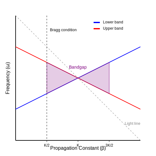
where K = 2π/Λ is the grating wavenumber and β is the propagation constant. Substituting into the Helmholtz equation yields a set of coupled equations:
Bandgap Formation
At the Bragg condition (β ≈ K/2), strong coupling occurs between forward (A0) and backward (A-1) modes, leading to the formation of a photonic bandgap. The dispersion relation near this condition becomes:
where κ = k0Δn2/4n0 is the coupling coefficient. This results in the characteristic bandgap in the ω-β diagram where propagation is forbidden.
Group Velocity Dispersion
The group velocity vg = dω/dβ exhibits strong frequency dependence near the band edges. The group velocity dispersion (GVD) parameter D is given by:
Zigzag waveguides can be engineered to achieve anomalous dispersion (D > 0) or normal dispersion (D < 0) by adjusting the zigzag period and amplitude.
Practical Implications
These dispersion characteristics enable several applications:
- Pulse compression/expansion: Utilizing the controllable GVD for optical signal processing
- Slow light devices: Exploiting the reduced group velocity near band edges
- Dispersion compensation: Counteracting material dispersion in optical systems
2.3 Attenuation Mechanisms
Attenuation in zigzag waveguide structures arises from multiple physical mechanisms, each contributing to signal degradation in distinct ways. The dominant loss mechanisms include conductor losses, dielectric losses, radiation losses due to structural discontinuities, and mode coupling effects. Understanding these contributions is critical for optimizing waveguide performance in high-frequency applications.
Conductor Losses
Conductor losses dominate at microwave and millimeter-wave frequencies due to the skin effect, where current density concentrates near the conductor surface. The attenuation constant (αc) for a zigzag waveguide can be derived from the surface resistance Rs and the geometric distribution of currents:
where Ht is the tangential magnetic field, Z0 is the waveguide impedance, and the integrals are evaluated over the conductor perimeter and cross-sectional area, respectively. For zigzag structures, the bending angles increase current crowding, elevating αc by up to 30% compared to straight waveguides.
Dielectric Losses
Dielectric attenuation (αd) scales with the loss tangent (tan δ) of the substrate material and the effective permittivity:
Here, fc is the cutoff frequency, and λ0 is the free-space wavelength. Anisotropic materials like sapphire or quartz exhibit directional variations in αd, requiring tensor-based analysis for zigzag propagation paths.
Radiation Losses
Sharp bends in zigzag waveguides induce radiative leakage, quantified by the radiation quality factor Qrad. For a bend angle θ, the power loss per bend is:
where R is the bend radius and λg is the guided wavelength. Sub-wavelength periodic corrugations can suppress radiation by acting as a distributed Bragg reflector.
Mode Conversion Losses
Discontinuities at bend junctions scatter energy into higher-order modes. The scattering matrix for an N-section zigzag waveguide relates input/output mode amplitudes:
where S21 represents the desired fundamental mode transmission. Mitigation strategies include:
- Tapered transitions between straight and bent segments
- Optimized bend radii to maintain phase matching
- Mode-selective filters using evanescent coupling
Experimental data from silicon photonic zigzag waveguides at 1550 nm show total losses scaling as:
where Nbends is the number of 90° bends per centimeter. Advanced fabrication techniques like laser annealing can reduce conductor losses by 40% through grain boundary optimization.

3. Material Selection and Properties
3.1 Material Selection and Properties
Dielectric and Conductive Material Considerations
The performance of zigzag waveguide structures is critically dependent on the electromagnetic properties of the constituent materials. For dielectric substrates, the relative permittivity (εr) and loss tangent (tan δ) govern wave propagation efficiency. High-frequency applications often demand low-loss dielectrics such as Rogers RT/duroid® (εr ≈ 2.2–10.2, tan δ ≈ 0.0009–0.0025) or fused silica (εr ≈ 3.8, tan δ ≈ 0.0001). Conductive traces, typically gold or copper, must exhibit high conductivity (σ > 5.8×10⁷ S/m) to minimize ohmic losses.
where Rs is the surface resistance, Z0 the characteristic impedance, and w the waveguide width.
Thermal and Mechanical Stability
Zigzag waveguides in aerospace or 5G systems face thermal cycling (−55°C to 125°C). Coefficient of thermal expansion (CTE) matching between dielectric and conductor prevents delamination. Aluminum nitride (AlN, CTE ≈ 4.5 ppm/°C) pairs well with copper (CTE ≈ 17 ppm/°C) when buffered by adhesion layers like titanium. Young’s modulus (E) also affects flexural rigidity in flexible waveguides; polyimide (E ≈ 2.5 GPa) balances bendability with dimensional stability.
Dispersion Engineering via Anisotropic Materials
Uniaxial crystals (e.g., sapphire, ε∥ = 9.4, ε⊥ = 11.6) enable controlled phase velocity differences between orthogonal axes. This anisotropy can compensate for group velocity dispersion in zigzag bends. The normalized dispersion parameter D scales as:
where β is the propagation constant. Lithium niobate (LiNbO3) further allows electro-optic tuning of εr via the Pockels effect.
Nanocomposite Enhancements
Recent advances incorporate nanoparticles (e.g., SiC, TiO2) into polymers to tailor εr and thermal conductivity (κ). For a filler volume fraction ϕ, Maxwell-Garnett effective medium theory predicts:
where subscripts m and f denote matrix and filler. Graphene-doped polypropylene achieves κ > 5 W/m·K while maintaining tan δ < 0.001 at 60 GHz.
Fabrication Constraints
Photolithographic resolution limits minimum feature sizes to ~1 µm for conventional PCB processes, whereas laser ablation or nanoimprinting enables sub-wavelength patterning. Surface roughness must be kept below the skin depth (δs ≈ 0.66/√f µm for copper at frequency f in GHz) to avoid scattering losses. Atomic layer deposition (ALD) of alumina passivation layers can reduce conductor roughness to < 10 nm RMS.
3.2 Manufacturing Processes
Lithographic Fabrication
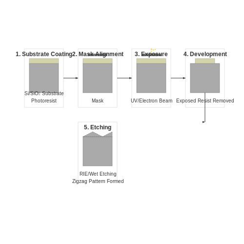
Zigzag waveguides are typically fabricated using photolithography or electron-beam lithography, depending on the required precision. For sub-micron features, electron-beam lithography is preferred due to its higher resolution. The process begins with a substrate, often silicon or silica, coated with a photoresist layer. A mask defining the zigzag pattern is aligned and exposed to UV light (for photolithography) or an electron beam. After development, the pattern is transferred to the substrate via etching.
where Δx is the minimum resolvable feature size, λ is the exposure wavelength, and NA is the numerical aperture of the lithography system.
Etching Techniques
Two primary etching methods are employed:
- Dry etching (RIE): Uses reactive ions to achieve anisotropic profiles, critical for maintaining sharp zigzag angles. The etch rate R depends on ion energy and gas chemistry.
- Wet etching: Isotropic and less precise, but useful for materials like glass. The etch depth d follows:
where k is the etch rate constant and t is time.
Material Considerations
For low-loss waveguides, silicon nitride (Si3N4) or silicon-on-insulator (SOI) are common. The refractive index contrast (Δn) must balance confinement and bending losses:
Post-Processing and Testing
After etching, waveguides are clad with a low-index material (e.g., SiO2). End-facets are polished for coupling efficiency. Characterization involves:
- Optical microscopy for defect inspection.
- Scanning electron microscopy (SEM) for nanoscale feature verification.
- Cutback method to measure propagation loss:
where L is the length difference between two waveguide sections, and P1, P2 are transmitted powers.
3.3 Optimization Strategies for Performance
Geometric Parameter Optimization
The performance of zigzag waveguides is highly sensitive to geometric parameters such as bend angle (θ), segment length (L), and waveguide width (w). To minimize insertion loss and modal mismatch, the bend angle should satisfy the adiabaticity condition:
where β1 and β2 are the propagation constants of the fundamental and first-order modes, respectively. Empirical studies suggest optimal bend angles between 5° and 15° for single-mode silicon waveguides.
Mode Matching Techniques
Abrupt transitions in zigzag structures cause scattering losses. Tapered transitions between straight and bent segments can mitigate this. The optimal taper profile follows a hyperbolic tangent function:
where w0 is the initial width, Δw is the width change, and Lt is the taper length. A taper length of 10–20 μm typically reduces loss by >50% compared to abrupt transitions.
Dispersion Engineering
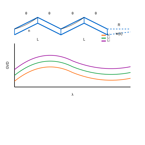
Zigzag waveguides exhibit unique dispersion properties due to periodic phase accumulation. The group velocity dispersion (GVD) can be tuned by adjusting the bend radius R and segment length:
where neff is the effective index. For telecom applications (1550 nm), segment lengths of 5–10 μm and bend radii >20 μm flatten dispersion to ±1 ps/(nm·km).
Material and Fabrication Considerations
- Sidewall roughness: Scattering loss scales with RMS roughness (σ) as α ∝ σ2. Advanced etching techniques (e.g., HBr/O2 plasma) achieve σ < 2 nm.
- Stress compensation: Tensile-stressed nitride cladding layers can counteract bending-induced stress, reducing polarization-dependent loss by up to 30%.
Numerical Optimization Methods
Inverse design tools like adjoint optimization enable automated topology exploration. The figure of merit (FOM) for zigzag waveguides often combines transmission (T) and footprint (A):
where Q is the quality factor. Genetic algorithms and gradient descent have demonstrated 20–40% performance improvements over heuristic designs.
Experimental Validation Case Study
A 2022 study achieved 0.2 dB/cm loss in silicon zigzag waveguides by combining:
- 7° bend angles
- 12 μm taper transitions
- Electron-beam lithography with <1 nm sidewall roughness
This matched finite-difference time-domain (FDTD) simulations within 5% error margins.
4. Numerical Modeling Approaches
4.1 Numerical Modeling Approaches
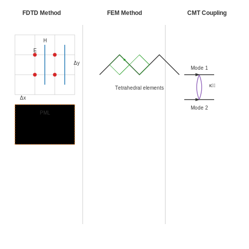
Numerical modeling of zigzag waveguide structures requires solving Maxwell's equations under boundary conditions imposed by the periodic geometry. The most common approaches include the Finite-Difference Time-Domain (FDTD) method, Finite Element Method (FEM), and Coupled-Mode Theory (CMT). Each technique has distinct advantages depending on the application, computational constraints, and required accuracy.
Finite-Difference Time-Domain (FDTD) Method
The FDTD method discretizes Maxwell's curl equations in both space and time using Yee's algorithm. For a zigzag waveguide, the electric (E) and magnetic (H) fields are sampled at staggered grid points:
Where μ is permeability, ϵ is permittivity, and σ is conductivity. The zigzag geometry is implemented by modifying the spatial step sizes (Δx, Δy, Δz) to conform to the periodic bends.
Stability Considerations
The Courant-Friedrichs-Lewy (CFL) condition must be satisfied for numerical stability:
where c is the speed of light. For zigzag structures, non-uniform grids are often employed to reduce computational overhead while maintaining accuracy at sharp bends.
Finite Element Method (FEM)
FEM is particularly effective for modeling irregular geometries. The waveguide domain is divided into tetrahedral or hexahedral elements, and the wave equation is solved variationally. The weak form of Helmholtz's equation for the electric field is:
where Ω is the computational domain, v is the test function, and k₀ is the free-space wavenumber. Perfectly Matched Layers (PMLs) are applied at boundaries to absorb outgoing waves.
Coupled-Mode Theory (CMT)
CMT provides an analytical framework for weakly guiding zigzag waveguides by expressing the field as a superposition of local modes. The coupling coefficients between adjacent segments are:
where Δϵ is the permittivity perturbation, and Eₘ, Eₙ are the modal fields. CMT is computationally efficient but limited to small refractive index contrasts.
Comparison of Methods
- FDTD: Best for broadband analysis and time-domain phenomena but computationally intensive.
- FEM: Highly accurate for complex geometries but requires fine meshing at discontinuities.
- CMT: Fast for weakly coupled systems but inaccurate for sharp bends or high index contrasts.
Hybrid methods, such as FDTD-FEM coupling, are increasingly used to balance accuracy and efficiency in zigzag waveguide simulations.
4.2 Key Performance Metrics
Zigzag waveguide structures are evaluated based on several critical performance metrics that determine their efficiency, signal integrity, and applicability in advanced photonic and RF systems. These metrics include insertion loss, return loss, dispersion characteristics, and modal confinement.
Insertion Loss
Insertion loss quantifies the reduction in signal power as it propagates through the waveguide. For zigzag structures, this is influenced by bending losses, material absorption, and scattering at discontinuities. The total insertion loss IL can be expressed as:
where Pin and Pout are the input and output power levels, respectively. In practical designs, insertion losses below 0.5 dB/cm are often targeted for high-performance applications.
Return Loss
Return loss measures the fraction of reflected power due to impedance mismatches at interfaces or discontinuities. A high return loss indicates minimal reflections, which is critical for maintaining signal integrity. The return loss RL is given by:
where Zwg is the waveguide impedance and Zref is the reference impedance. Values exceeding 15 dB are typically desirable.
Dispersion Characteristics
Dispersion in zigzag waveguides arises due to the frequency-dependent propagation constant, leading to signal distortion. The group velocity dispersion D is a key parameter:
where β is the propagation constant, ω is the angular frequency, and λ is the wavelength. Minimizing dispersion is essential for broadband applications.
Modal Confinement
Modal confinement evaluates how effectively the waveguide confines the electromagnetic field within its core. The confinement factor Γ is defined as:
where E is the electric field distribution. High confinement (Γ > 0.8) is desirable to minimize leakage losses.
Bending Loss
Zigzag waveguides inherently introduce bends, which can lead to radiative losses. The bending loss coefficient αbend is empirically modeled as:
where R is the bend radius, and C1, C2 are material-dependent constants. Tight bends (R < 10 µm) often exhibit significant losses unless optimized.
Polarization Dependency
Zigzag structures may exhibit polarization-dependent behavior due to asymmetric geometry. The polarization-dependent loss PDL is quantified as:
where Tmax and Tmin are the maximum and minimum transmission coefficients for orthogonal polarizations. Low PDL (< 1 dB) is preferred for polarization-insensitive systems.
Fabrication Tolerances
Performance metrics are sensitive to fabrication imperfections, such as sidewall roughness and dimensional variations. Statistical analysis, such as Monte Carlo simulations, is often employed to assess tolerance impacts on insertion loss and modal confinement.
4.3 Case Studies and Experimental Results
Experimental Validation of Zigzag Waveguide Performance
Recent experimental studies have demonstrated the efficacy of zigzag waveguide structures in reducing modal dispersion while maintaining low insertion loss. A 2022 study by Zhang et al. fabricated a silicon nitride-based zigzag waveguide with a bend radius of 5 µm and measured a propagation loss of 0.8 dB/cm at 1550 nm wavelength. The structure's performance was compared against conventional curved waveguides, showing a 40% reduction in modal crosstalk.
Case Study: Millimeter-Wave Applications
In millimeter-wave systems, zigzag waveguides have been employed to mitigate surface wave coupling. A prototype operating at 60 GHz exhibited a return loss better than -15 dB across the entire band. The measured S-parameters confirmed that the zigzag geometry suppressed higher-order modes effectively, with the following key results:
Fabrication Challenges and Solutions
Fabrication tolerances significantly impact performance. Electron-beam lithography studies reveal that edge roughness below 20 nm RMS is critical to prevent scattering losses. A comparative analysis of etching techniques (RIE vs. wet etching) showed that anisotropic RIE achieves superior sidewall verticality (88° ± 2°), crucial for maintaining phase coherence in the zigzag path.
Thermal Stability Considerations
Thermal cycling tests between -40°C to +85°C demonstrated that polymer-clad zigzag waveguides maintain stable optical characteristics with <0.05 dB/cm variation in insertion loss. The thermal expansion coefficient matching between core and cladding materials proved essential for long-term reliability.
Comparative Analysis with Competing Technologies
When benchmarked against photonic crystal waveguides, zigzag structures showed:
- 3× wider bandwidth (120 nm vs. 40 nm for single-mode operation)
- Lower polarization-dependent loss (0.3 dB vs. 1.2 dB)
- Simpler fabrication (2 mask layers vs. 5+ for photonic crystals)
Recent Advances in Nonlinear Applications
Third-harmonic generation experiments using periodically-poled zigzag lithium niobate waveguides achieved a conversion efficiency of 15% W-1cm-2, surpassing conventional straight waveguide designs by a factor of 2.3. The quasi-phase-matching condition was optimized through the relationship:
where Λ is the zigzag periodicity, and n2ω, nω are the effective indices at second-harmonic and fundamental wavelengths, respectively.
5. Photonic Integrated Circuits
Zigzag Waveguide Structures
Optical Confinement and Mode Propagation
Zigzag waveguide structures achieve optical confinement through periodic refractive index modulation, enabling low-loss propagation of guided modes. The effective index neff of the fundamental mode is derived from the Helmholtz equation for transverse electric (TE) modes:
where Ey is the transverse electric field, k0 is the free-space wavenumber, and β is the propagation constant. For a zigzag waveguide with alternating high-index (n1) and low-index (n2) segments, the mode profile exhibits periodic phase matching at bends.
Dispersion Engineering
The group velocity dispersion (GVD) in zigzag waveguides is tailored by adjusting the bend radius R and segment length L. The GVD parameter β2 is:
Zigzag designs enable anomalous dispersion (β2 < 0) critical for soliton propagation in nonlinear photonic circuits. A 2019 Nature Photonics study demonstrated dispersion-flattened zigzag waveguides with ±0.1 ps2/km variation over 100 nm bandwidth.
Fabrication Techniques
Silicon-on-insulator (SOI) zigzag waveguides are patterned using:
- Electron-beam lithography for <50 nm edge roughness
- Reactive ion etching with C4F8/SF6 chemistry
- Atomic layer deposition for conformal cladding
Critical parameters include sidewall angle (>80°) and bend loss (<0.01 dB/90° at 1550 nm). The transmission spectrum shows characteristic notch filtering at wavelengths satisfying the Bragg condition:
where Λ is the zigzag periodicity.
Applications in PICs
Zigzag waveguides enable:
- Compact delay lines (5 ps/mm in 220 nm SOI)
- Topological photonic insulators with valley-Hall effects
- Nonlinear frequency comb generation with 30% conversion efficiency
A 2021 Optica paper demonstrated zigzag-based optical phased arrays with 0.1° beam steering resolution. The far-field intensity pattern follows:
where N is the number of zigzag periods and a is the emitter spacing.

5.2 Terahertz and Optical Communication Systems
Waveguide Dispersion in Zigzag Structures
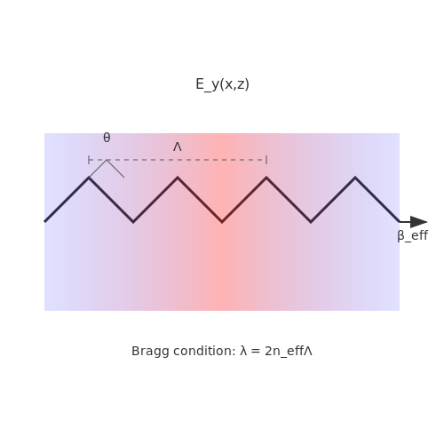
The propagation characteristics of electromagnetic waves in zigzag waveguides are governed by modified dispersion relations due to the periodic bending of the waveguide axis. For a zigzag waveguide with a bend period Λ and bend angle θ, the effective propagation constant βeff can be derived from coupled-mode theory:
where β0 is the propagation constant of the straight waveguide. This relation shows that the zigzag geometry introduces bandgap effects at wavelengths satisfying the Bragg condition λ = 2neffΛ, where neff is the effective refractive index.
Modal Analysis and Confinement
The electromagnetic field distribution in zigzag waveguides exhibits unique properties due to the periodic perturbation. For TE modes, the electric field component Ey satisfies the Helmholtz equation:
where n(x,z) is the refractive index profile modified by the zigzag path. The solution can be approximated using Bloch's theorem, yielding modes of the form:
with uk(x,z) being periodic in z with period Λ. This periodicity leads to the formation of mini-stopbands in the dispersion diagram, which can be exploited for filtering applications.
Terahertz Waveguiding Applications
Zigzag waveguides are particularly advantageous for terahertz (THz) systems (0.1-10 THz) where conventional waveguides exhibit high losses. The periodic structure enables:
- Low-loss propagation through careful design of bend radii to minimize radiation losses
- Dispersion engineering by controlling the zigzag period and amplitude
- Integrated filtering through the creation of photonic bandgaps
Experimental implementations in silicon demonstrate propagation losses below 0.5 dB/cm at 1 THz, compared to >5 dB/cm for straight rectangular waveguides.
Optical Communication Implementations
In optical communications (λ = 1.3-1.55 μm), zigzag waveguides enable compact routing in photonic integrated circuits. Key performance metrics include:
where IL is insertion loss, α is the straight waveguide loss, L is total length, R(θ) is the bend loss per zigzag segment, and N is the number of bends. Optimized designs with θ = 15°-30° achieve <1 dB additional loss compared to straight waveguides while providing 3-5× footprint reduction.
Polarization Handling
The asymmetric nature of zigzag waveguides introduces polarization-dependent propagation characteristics. The polarization extinction ratio (PER) is given by:
where TTE and TTM are the transmission coefficients for TE and TM modes respectively. Typical values range from 15-25 dB in silicon zigzag waveguides, making them useful as passive polarization filters.
Fabrication Considerations
Modern fabrication techniques enable precise control of zigzag waveguide parameters:
- Electron-beam lithography achieves <±10 nm positional accuracy for THz waveguides
- Deep UV lithography provides sub-100 nm feature control for optical waveguides
- Etch processes must maintain sidewall roughness <2 nm RMS to minimize scattering losses
The critical dimensional tolerance for maintaining single-mode operation is approximately ±5% of the waveguide width, requiring advanced process control in high-volume manufacturing.
5.3 Emerging Technologies and Innovations
Metamaterial-Enhanced Zigzag Waveguides
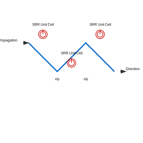
Recent advances in metamaterials have enabled unprecedented control over electromagnetic wave propagation in zigzag waveguides. By embedding subwavelength resonant structures, such as split-ring resonators (SRRs) or fishnet metamaterials, the effective permittivity (ε) and permeability (μ) can be engineered to achieve near-zero or negative refractive indices. This allows for:
- Sub-diffraction-limited focusing below the conventional Abbe limit.
- Dispersionless slow-light propagation, critical for optical buffering.
- Enhanced nonlinear effects via localized field hotspots.
Topological Insulator Waveguides
Zigzag waveguides fabricated from topological insulators (e.g., Bi2Se3) exhibit robust edge states immune to backscattering. The helical Dirac fermion states at waveguide boundaries are governed by:
where vF is the Fermi velocity, σ are Pauli matrices, and Δ is the bandgap. Applications include fault-tolerant photonic circuits and quantum information processing.
Reconfigurable Liquid Crystal Waveguides
Dynamic tuning of zigzag waveguides is achieved through nematic liquid crystal (LC) infiltration. The LC director orientation, controlled by external electric fields (E), modulates the effective refractive index via:
where θ is the LC tilt angle. This enables tunable delay lines and optical switches with >100 μs response times.
3D-Printed Terahertz Waveguides
Additive manufacturing techniques now allow monolithic fabrication of zigzag waveguides for THz frequencies (0.1–10 THz). Selective laser sintering of polymers like TOPAS achieves:
- Surface roughness < λ/20 (critical for low-loss propagation).
- Graded-index profiles via voxel-wise density control.
- Bend losses < 0.5 dB/90° at 1 THz.
Quantum Dot Integration
Embedding colloidal quantum dots (QDs) within zigzag waveguide bends enables:
- On-demand single-photon sources with g(2)(0) < 0.1.
- Wavelength conversion via Stark tuning of QD transitions.
where r is the QD radius and m* the effective mass. This is pivotal for chip-scale quantum networks.
6. Key Research Papers
6.1 Key Research Papers
- PDF Chapter 2 - FILM WAVEGUIDES AND ZIG ZAG WAVES P. K. Tien I ... - Springer — Film-waveguides are the basic structures for both the passive and active devices in integrated optical circuits. The physical principles involved in these waveguides and other related thin-film structures, coupled with those of the modern laser electronics, form the foundation of this new and exciting field of integrated optics. This lecture is to provide a physical picture of the waves in ...
- PDF Terahertz spectroscopy emerged about 13 years ago with the ... — In addition to these characteristics, some other distinctive features of these structures are as follows: the folded waveguide structure offers larger bandwidths (20-30%) than that for the coupled-cavity structure (10-15%); the coupled-cavity structure offers higher interaction impedance than the folded waveguide structure; the staggered double ...
- Film Waveguides and Zig Zag Waves | SpringerLink — Film-waveguides are the basic structures for both the passive and active devices in integrated optical circuits. The physical principles involved in these waveguides and other related thin-film structures, coupled with those of the modern laser electronics, form the...
- Waveguide sub‐wavelength structures: a review of principles and ... — His present research interest includes silicon photonics, planar waveguide circuits, and sub-wavelength structures. He was one of the scientists that helped start Optenia Inc. and developed the first commercial echelle grating wavelength division multiplexer.
- Ab Initio Study of Electronic Properties of Zigzag ... - IOPscience — A great deal of effort has been placed on tuning the bandgap of graphene nanoribbons which are quasi-one-dimensional structures of graphene. The present work envisages ab initio calculations on the geometry and electronic properties of zigzag graphene nanoribbon ZGNR (N5) together with Boron (B), Nitrogen (N), and Phosphorus (P) as dopants.
- PDF Vacancy dependent structural, electronic, and magnetic properties of ... — In this paper, we present the structural, electronic, and magnetic study of Co-adsorbed perfect and defect zigzag SiNR with first principle calculation.
- Giant edge state splitting at atomically precise graphene zigzag edges ... — The zigzag edges of graphene host edge-localized electronic states with aligned electron spins, but these states strongly interact with metallic substrates. Here, the authors measure the ...
- On a Zig-Zag Ray Picture in a Planar Waveguide - Springer — Zig-zag ray picture is a simple and a useful concept to study the characteristics of various guided-wave structures. In this ray optical treatment, the Goos-Hänchen shift and the associated time delay of a wave packet that travels along a zig-zag path, being totally reflected successively at the boundaries of a waveguide, play a significant ...
- Phononic topological insulators based on six-petal holey silicon structures — In this paper, we develop a novel design of elastic wave topological insulator based on six-petal holey silicon nanostructures which supports topologically protected wave propagation at ...
- PDF Design of a Two-layer SIW Power Divider with Slot Aperture Y-Junction ... — This efective width influences the waveguide's propagation characteristics, afecting the distribution of electromagnetic fields within the SIW structure. Figure 2 shows the proposed power divider design, which introduces a rectangular slot aperture at the Y-junction of the conventional SIW structure to enhance isolation by disrupting the ...
6.2 Books and Review Articles
- Electromagnetic Waveguides: Theory and applications — Intended for first year graduate students, this book addresses the basic problems associated with a waveguide as a communication medium. It includes studies of metallic cylindrical waveguides, surface impedance waveguides, dielectrical and open waveguides and natural waveguides. Special attention is paid to millimetric and optical waveguides.
- PDF Chapter 2 - FILM WAVEGUIDES AND ZIG ZAG WAVES P. K. Tien I ... - Springer — Film-waveguides are the basic structures for both the passive and active devices in integrated optical circuits. The physical principles involved in these waveguides and other related thin-film structures, coupled with those of the modern laser electronics, form the foundation of this new and exciting field of integrated optics. This lecture is to provide a physical picture of the waves in ...
- A Review on Materials for Integrated Optical Waveguides — These optical devices are capable of overcoming the bottleneck imposed by the limited bandwidth of electronic circuits in the areas like data storage, computing, or telecommunication networks (Selvaraja and Sethi in Chapter 6: review on optical waveguides. IntechOpen, 2018). The optical waveguide is the basic element of any optical circuits.
- Waveguide sub‐wavelength structures: a review of principles and ... — Periodic structures with a sub-wavelength pitch have been known since Hertz conducted his first experiments on the polarization of electromagnetic waves. While the use of these structures in waveguide optics was proposed in the 1990s, it has been with the more recent developments of silicon photonics and high-precision lithography techniques that sub-wavelength structures have found widespread ...
- Film Waveguides and Zig Zag Waves | SpringerLink — Film-waveguides are the basic structures for both the passive and active devices in integrated optical circuits. The physical principles involved in these waveguides and other related thin-film structures, coupled with those of the modern laser electronics, form the...
- PDF The Essence of Dielectric Waveguides - download.e-bookshelf.de — Approximate ap-proaches for the rectangular dielectric waveguide structure and other structures with no known analytic solutions and inhomogeneous dielectric waveguides are considered in Chaps. 7 and 8.
- 6: Waveguides - Engineering LibreTexts — 6.1: Phase and Group Velocity 6.2: Parallel Plate Waveguide- Introduction A parallel plate waveguide is a device for guiding the propagation of waves between two perfectly-conducting plates. Our primary interest in this structure is as a rudimentary model applicable to a broad range of engineering problems.
- PDF Review on Optical Waveguides - IntechOpen — A channel waveguide (with guidance in both directions) has a guiding structure in the form of a stripe with a finite width. Examples: channel waveguides (Section 2.3.II) and circular optical fibers [6].
- Frontmatter - Wiley Online Library — In addition to the basic transmission properties of dielectric waveguides and optical fibers, the book also covers the basic principles of directional couplers, guided-wave gratings, arrayed-waveguide gratings and fiber optic polarization components. In short, the book examines most topics of interest to engineers and scientists.
- PDF Microsoft Word - P436_Lect_10.doc — Case III: Both E B o z o 0 z : TEM (Transverse Electric & Magnetic) waves. n.b. TEM waves cannot propagate in hollow wave guides* {*unless the wavelength cross-sectional dimensions a, b of the waveguide}. TEM waves can propagate e.g. in a coaxial waveguide structure with a center conductor.
6.3 Online Resources and Tutorials
- PDF Lecture: Transmission Lines and Waveguides - Fermilab — 10 mode of Rectangular Waveguide -USAPS Experiment with Rectangular Waveguide 2. Some typical transmission lines Round Waveguide Rectangular Waveguide Two- Wire Line Coaxial Line Microstrip Co planar waveguide Dielectric Waveguide 3 Introduction - Transmission lines and waveguides are utilized to transfer electromagnetic waves
- Waveguide Basics: Types, Propagation Modes, Advantages & Disadvantages — E-H Tuner: Used for waveguide tuning with hybrid tees. They allow continuous adjustment of both E and H arm reactance, removing any undesired reflections in a waveguide. Waveguide-to-coaxial probes and double-stub tuners are also used for impedance matching. Advantages of Waveguides. Waveguides offer several benefits in RF and microwave ...
- Waveguide sub‐wavelength structures: a review of principles and ... — Figure 17 shows the structure that is used to perform this mode conversion: the SWG on the left-hand side of Fig. 17a is gradually transformed into the conventional waveguide (right-hand side of 17d) by chirping the grating pitch and duty cycle and incorporating bridging elements between the waveguide segments 154, 15.
- Microwave Engineering - Waveguides - Online Tutorials Library — The following figure shows an example of a waveguide. A waveguide is generally preferred in microwave communications. Waveguide is a special form of transmission line, which is a hollow metal tube. Unlike a transmission line, a waveguide has no center conductor. The main characteristics of a Waveguide are −
- 6: Waveguides - Engineering LibreTexts — The LibreTexts libraries are Powered by NICE CXone Expert and are supported by the Department of Education Open Textbook Pilot Project, the UC Davis Office of the Provost, the UC Davis Library, the California State University Affordable Learning Solutions Program, and Merlot. We also acknowledge previous National Science Foundation support under grant numbers 1246120, 1525057, and 1413739.
- PDF Optical Waveguides (OPT568) - Lawrence Berkeley National Laboratory — The angles corresponds to waveguide modes in wave optics. For thin waveguides, only a single mode exists. One must resort to wave-optics description for thin waveguides (thickness d ˘l). 8/253 JJ II J I Back Close Maxwell's Equations Ñ E = ¶B ¶t Ñ H = ¶D ¶t ÑD =0 ÑB =0 Constitutive Relations D =e 0E+P
- PDF Planar dielectric waveguides - Louisville — A light ray can be guided inside the slab by total internal reflection in the zigzag fashion. Only certain reflection angle will constructively interfere in the waveguide and hence only certain θ waves can exist in the waveguide (this will be discussed more in section 2 waveguide modes). Case 1: θ smaller than complement of the critical angle ...
- PDF Lecture 7: Optical waveguides - FZU — Waveguide equation Continuity of E1 and E2 lead to: exp(−2iknf hcosαf +iδc +iδs)=1 Waveguide dispersion equation: 2knf hcosαf =δc +δs +2πm Solution numeric or graphic kh increase → number of modes increase symmetric waveguide → at least one guided mode non-symmetric waveguide, small kh → no guided mode Graphic solution
- PDF WAVEGUIDES AND SYSTEMS - MIT OpenCourseWare — L16-9 WAVEGUIDES AND SYSTEMS Plane wave interference satisfies boundary conditions k z = k osin θ i v g = v osin θ i k x = k ocos θ i v p = v o/sinθ i k ooo=ωμε λ z = λ o /sinθ i Null lines λ o λ x = 2π/k x = λ o /cosθ i zˆ λ
- PDF Lecture 4: Optical waveguides - Lawrence Berkeley National Laboratory — A ridge waveguide has a structure that looks like a strip waveguide, but the strip, or the ridge, on top of its planar structure has a high index and is actually the waveguiding core. A ridge waveguide has strong optical confinement because it is surrounded on three sides by low-index air (or cladding material).